
Wire Bonding in Altium Designer
The primary objective of wire bonding is to establish a secure and low-resistance electrical connection between a semiconductor chip and its package or between different chips within a multi-chip module. This process involves bonding a fine wire, typically made of gold, aluminum, or copper, from the bond pad on the chip to a corresponding pad on the package substrate or another chip.
Wire bonding transmits power and signals between substrates and chips. It is the basic technology in which an electrical connection between the chip contact surfaces (pads) and the chip carrier or substrate is established by the micro-welding of micro-wires. it is generally considered the most cost-effective and flexible interconnect technology and is used to assemble most semiconductor packages.
Altium Designer supports the design of hybrid boards with chip-on-board (CoB) technology using Wire Bonding. This feature allows you to create a component with defined Die Pads and, once placed on a schematic and synchronized (through ECO) to the PCB, can be wired to regular pads (or any copper) on the main board using Bond Wires. When connected to a regular pad, that pad takes on the likeness of a Bond Finger pad.
Chip-on-Board Component Footprint Creation
You can define a complete, simple package with defined die pads, bond finger pads, and bond wires, all as part of the component footprint.
Die pads and die 3D bodies are placed on a layer of a dedicated Die component layer pair. A component layer pair of this type can be added using the View Configurations panel.
Learn more about adding component layer pairs.

Die pads are placed on an extruded 3D body on the Die layer (referred to as a Die Body). The die pad will be automatically placed at the Overall Height of the die body and it will be bound to it by height.


Place regular pad objects placed on a copper layer (e.g., the Top Layer). After connecting bond wires to them, these pads will be considered bond finger pads.

In this example, pads placed on the Top Layer around the die will act as bond finger pads.
 ).
).Bond wires are placed on a layer of a dedicated Wire Bonding component layer pair that can also be added using the View Configurations panel.

Use the Place » Bond Wire command or the ![]() icon on the Active Bar to place a bond wire. After selecting the command, sequentially click two points you want to connect with a bond wire (e.g., the center point of a die pad and the center point of a finger pad). A straight line, which is a projection of the bond wire to the XY plane, will be shown in 2D. In 3D, the bond wire is rendered based on the position of its start and end points and other properties.
icon on the Active Bar to place a bond wire. After selecting the command, sequentially click two points you want to connect with a bond wire (e.g., the center point of a die pad and the center point of a finger pad). A straight line, which is a projection of the bond wire to the XY plane, will be shown in 2D. In 3D, the bond wire is rendered based on the position of its start and end points and other properties.


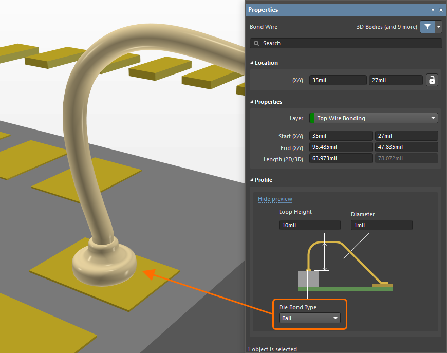
Use the fields in the Profile region of the Properties panel to specify the desired values of the Loop Height and Diameter of a bond wire, as well as the Die Bond Type that defines the shape at the bond wire's start point (Ball or Wedge).

If bond finger pads need to be oriented so that a longer side of a pad is in parallel with the connected bond wire, you can select bond wires and bond finger pads connected to them, right-click the selection, and then choose the Pad Actions » Align Bond Finger with Bond Wire command from the right-click menu.


An example of a complete footprint that features wire bonding is shown below.

Placing Wire Bonds in a PCB
When using the Chip-on-Board approach, you can also place bond wires manually (in the same way as described above) to connect the die pads of the chip to any copper on the main board. A bond wire will inherit the net of its source die pad. Multiple bond wires can emanate from the same die pad and, conversely, multiple bond wires can finish on the same copper on the main board.
An example of a PCB that features wire bonding is shown below.

 ).
).Design Rules Checks for Wire Bonding
A Wire Bonding design rule (the Routing category) can be defined in the All Rules view of the Constraint Manager when accessed from a PCB and the PCB Rules and Constraints Editor dialog (when using the older approach to design rule definition and management). The rule enables constraints to be defined for the permissible distance between adjacent bond wires (Wire To Wire), Min Wire Length and Max Wire Length, and Bond Finger Margin, which is the distance/padding between a bond wire and the edge of the bond finger pad to which it is wired. The Wire Bonding design rule is supported by the batch DRC.

A Wire Bonding rule defined in the Constraint Manager

A Wire Bonding rule defined in the PCB Rules and Constraints Editor dialog
Electrical rule checks (Un-Routed Net and Short Circuit) also apply to Wire Bonding.


Wire Bonding Query Keywords
The following query language keywords are available for use in logical query expressions when creating design rule scopes (in both the Constraint Manager and the PCB Rules and Constraints Editor dialog), as well as when constructing query expressions to use in the filtering of objects in a PCB or PCB library:
-
IsBondFinger – returns an SMD pad primitive on a copper layer that has a bond wire connected to it.
-
IsBondWire – returns a bond wire primitive.
-
IsBondWireConnected – returns any primitive that has a bond wire connected to it.
Wire Bonding in a Draftsman Document
Draftsman supports wire bonding in both its regular board assembly view (for the main Chip-on-Board approach) and also the component view (for where the wire bonding 'package' has been fully defined within the footprint).
-
Enable layers for die pads and bond wires on the Layers tab of the Properties panel of the selected board assembly view to show these layers on the view (and derived board detail views, as shown below).

-
When a component features wire bonding (i.e., it has die pad(s) and bond wires connected to them), additional Bond Wires and Die Pads options are available in the Properties region of the Properties panel for the selected component view placed for this component. Use these options to enable graphics of bond wire projections and die pads, respectively.

Wire Bonding Outputs
Wire bonding information is supported when generating regular PCB Prints. By configuring layers and designators to be printed, you can form a wire bonding diagram.

An example of a PCB print configured as a wire bonding diagram.
Also, a Wire Bonding Table Report that provides information in relation to bond wire connections can be generated (in the CSV format). Use the Wire Bonding Table Report output from the Assembly Outputs region of an Output Job file to add a new output of this type. Alternatively, select the File » Assembly Outputs » Wire Bonding Table Report command from the main menus of the PCB editor to generate the report directly from the editor.

Add a new Wire Bonding Table Report output to the Outjob file.

An example of a generated Wire Bonding Table Report