
Altium Designer의 새로운기능
이 페이지에서는 Altium Designer, Altium Designer Develop, Altium Designer Agile 릴리스에 포함된 개선 사항을 자세히 설명합니다. 기존 기술을 발전·성숙시키는 다양한 개선 사항을 제공하는 것과 함께, 각 업데이트에는 AltiumLive Community의 BugCrunch 시스템을 통해 고객이 제기한 피드백을 바탕으로 소프트웨어 전반에 걸친 여러 수정 및 향상이 포함되어, 최첨단 전자 기술을 계속 개발할 수 있도록 지원합니다.
버전 26.1
Altium Designer – Released: 3 December 2025 – Version 26.1.0 (build 7)
PCB 설계 개선
솔더 마스크 확장 규칙 기본값이 이제 0 mils (Open Beta)
패드스택 기본값과 관련하여 IPC-7351B 표준(솔더 마스크 오프닝이 일반적으로 랜드 크기와 1:1 비율)을 준수함에 따라, 이제 솔더 마스크 확장 규칙(PCB 문서) 및 규칙 기반 솔더 마스크 확장(PCB 라이브러리 문서)의 값이 기본적으로 0 mil로 설정됩니다(기존 4 mil).
PCB 라이브러리(*.PcbLib

PCB 문서(*.PcbDoc

Constraint Manager에서 새로 생성된 Solder Mask Expansion 설계 규칙.

Solder Mask Expansion 설계 규칙에 대한 자세한 내용은 Mask Rule Types 페이지를 참조하세요.
Constraint Manager 개선
클래스 필터링 기능 추가
Constraint Manager의
![]() 버튼을 사용하면 팝업을 열어 필터를 생성, 편집, 제거, 활성화/비활성화할 수 있습니다.
버튼을 사용하면 팝업을 열어 필터를 생성, 편집, 제거, 활성화/비활성화할 수 있습니다.
![]()
새 필터를 만들려면 ![]() 버튼을 클릭한 다음, 표시되는 팝업에서
버튼을 클릭한 다음, 표시되는 팝업에서 ![]() 버튼을 클릭합니다.
버튼을 클릭합니다.
![]()
새 필터의 고유한 이름을 정의하고 필요한 클래스 그룹을 활성화한 뒤 ![]() 을(를) 클릭합니다.
을(를) 클릭합니다.
![]()
필터를 생성한 후에는 팝업의 컨트롤을 사용해 필요에 따라 활성화, 비활성화, 편집 또는 제거할 수 있습니다. 필터가 활성화되면 오른쪽 상단의 버튼이 ![]() (으)로 표시됩니다.
(으)로 표시됩니다.
클리어런스 매트릭스 작업에 대한 자세한 내용은 Defining Design Requirements Using the Constraint Manager 페이지를 참조하세요.
Draftsman 개선
Draftsman 문서로의 DXF 가져오기 향상 (Open Beta)
이 기능은 제조 도면 문서(*.PCBDwf*.HarDwf*.MbDwf
DXF 파일 가져오기에 대한 자세한 내용은 Draftsman Placement & Editing Techniques 페이지를 참조하세요.
와이어 본딩 개선
패널에서 Bond Wire 프리미티브 표시
이제 본드 와이어가 다음 위치에서 올바른 유형(
-
풋프린트를 선택했을 때 PCB Library panel.
본드 와이어 프리미티브를 선택하면 설계 공간에서 해당 본드 와이어가 선택/강조 표시됩니다.


또한 본드 와이어 가시성을 전환할 수 있도록, 영역의 우클릭 컨텍스트 메뉴에 해당
와이어 본딩에 대한 자세한 내용은 Wire Bonding 페이지를 참조하세요.
3D-MID 설계 개선
3D-MID 설계 규칙 검사(DRC) (Open Beta)
이번 릴리스에서는 3D 기판 위에 라우팅된 트랙에 대해 Width, Clearance, Length, Matched Lengths 규칙 위반을 일괄로 DRC 수행할 수 있습니다. 생성된 DRC 보고서는 이러한 모든 검사에 대한 정보를 제공하지만, 설계 공간에서 하이라이트되는 것은 클리어런스 위반만이라는 점에 유의하세요.


자세한 내용은 3D-MID Design 페이지를 참조하세요.
멀티보드 설계 개선
하네스 엔트리에 ‘Termination Type’ 정의 기능
이제 멀티보드 회로도에서 하네스 엔트리의
-
Connector – PCB의 메이팅 커넥터에 연결할 때 사용하는 표준 옵션입니다. 일반적으로 표준 보드 장착형 커넥터가 포함됩니다. -
Crimps/Ferrules – 개별 와이어를 PCB 측 커넥터에 삽입하기 전에 크림프(crimp) 또는 페룰(ferrule)로 종단 처리합니다. -
Wire termination – 하네스 끝단에서 와이어를 단순 절단(blunt-cut)한 뒤, 나사로 고정하거나 PCB에 직접 납땜합니다. 일부 JST 커넥터처럼 와이어-투-보드 직접 연결에서 흔히 사용됩니다.
이 정보는 선택된 하네스 엔트리의 속성과 해당 모듈 엔트리의 속성에 반영됩니다.


멀티보드 회로도에서 연결 작업에 대한 자세한 내용은 Working with Connections 페이지를 참조하세요.
하네스 설계 개선 사항
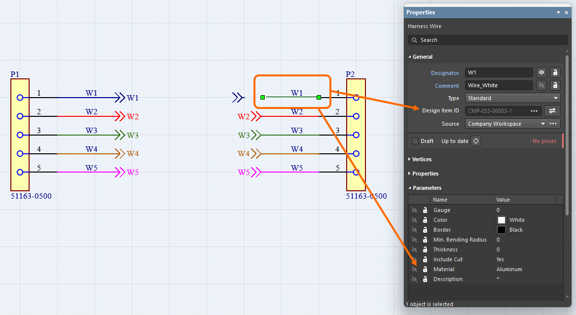
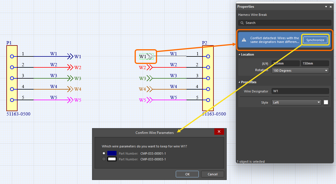
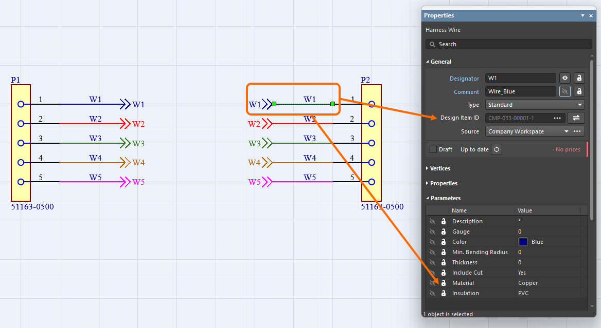
와이어 동기화 향상
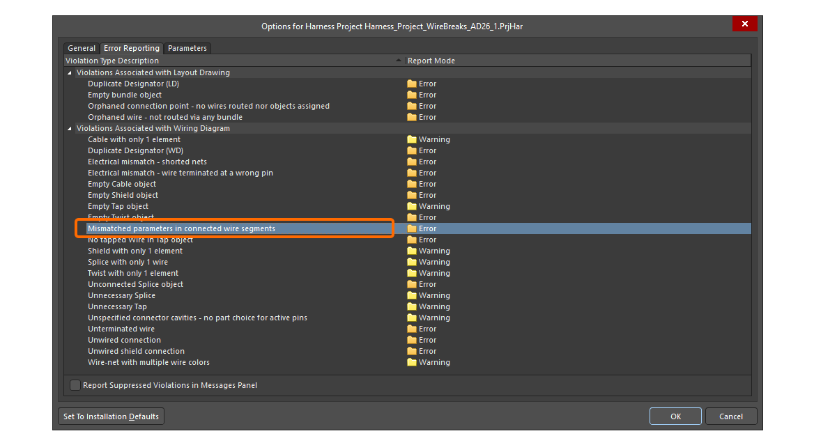
이제 와이어 브레이크로 연결된 하네스 와이어는 Design Item ID가 서로 달라도 인식됩니다. 또한 동일한 와이어 브레이크로 연결된 동일한 설계자(designator)의 모든 와이어 세그먼트가 (부품 번호, 코멘트, 색상 및 모든 파라미터에 대해) 비교됩니다. 차이가 발견되면 Mismatched parameters in connected wire segments
접합 지점 위에 커버링 배치 기능
이제 하네스 레이아웃 도면(*.LdrDoc

또한 커버링의 시작점은 이제 경로에서 가장 왼쪽, 가장 위쪽 지점으로 간주되며, 해당 경로에는 커버링이 놓이는 번들만 포함되도록 변경되었습니다.
자세한 내용은 Creating the Layout Drawing 페이지를 참조하세요.
특정 객체의 BOM 수량 필드가 'As Required'로 변경됨
와이어, 케이블 및 하네스 커버링은 길이 기반 객체이며 값은 *.HarDwfAs Required

자세한 내용은 Managing Your Bill of Materials (BOM) with ActiveBOM 페이지를 참조하세요.
배선 목록에서의 핀 그룹화 개선
하네스 제조 문서(*.HarDwf

하네스 제조업체용 Excel 통합 문서
Output Job을 통해 하네스 제조업체가 사용할 데이터를 포함한 단일 Excel 통합 문서를 생성하는 기능이 추가되었습니다. 이를 위해

생성된 통합 문서에는 다음 4개의 개별 시트가 포함됩니다:
-
Bill of Materials – 빠른 견적 산출에 유용합니다. -
Wiring List – 와이어 가공 장비에서 사용합니다. -
Labels – Zebra 또는 기타 프린터로 하네스 번들에 부착할 물리적 라벨을 인쇄하기 위한 요약입니다. -
Coverings – 하네스 번들 위에 적용할 커버링에 대한 요약입니다.


자세한 내용은 Preparing Reports 페이지를 참조하세요.
플랫폼 개선
.NET 8로 전환
이번 릴리스에서 Altium Designer는 .NET 6 사용에서 .NET 8 사용으로 전환합니다. .NET 8은 Altium Designer에 번들로 포함되며, 전반적인 성능 향상을 포함해 .NET의 최신 기능과 개발 사항을 활용할 수 있게 해줍니다.
자세한 내용은 System Requirements 페이지를 참조하세요.
WebView2 (Open Beta)
이번 릴리스부터 Altium Designer 내의 브라우저 관련 요소(예:
데이터 관리 개선
프로세스 워크플로를 사용한 Workspace 프로젝트 복사 기능
정의(및 활성화)된 프로세스 워크플로를 사용하여 Workspace 프로젝트의 복사본을 만드는 기능이 추가되었습니다. Workspace 프로젝트를 열면

자세한 내용은 Process-based Project Creation 페이지를 참조하세요.
모델 릴리스 시 라이프사이클 상태 유지 기능 추가
연결된 Workspace에 컴포넌트 모델의 새 리비전(schematic symbol, PCB footprint, simulation model 또는 harness wiring)을 릴리스할 때, 이제 모델의 현재 라이프사이클 상태를 유지할 수 있습니다.

이 기능은
Workspace 콘텐츠 편집에 대한 자세한 내용은 Creating & Editing Content 페이지를 참조하세요.
설계 검토 코멘트 링크
설계 검토의 일부로 코멘트가 추가되면, 해당 검토(From <DesignReviewName>

문서 코멘팅에 대한 자세한 내용은 Document Commenting 페이지를 참조하세요.
추가 단위 인식 데이터 타입 지원
Altium Platform의 연결된 Workspace에서 컴포넌트 템플릿의 일부로 사용자 파라미터를 정의할 때, 이제 다음의 추가 단위 인식 데이터 타입이 지원됩니다:
-
면적 (mm2)
-
Bar (bar)
-
Bit
-
Candela (cd)
-
Decimal
-
Integer
-
Joule (J)
-
Lumen (lm)
-
Millimetre (mm)
-
Pascal (Pa)
-
제곱인치당 파운드 (psi)
-
분당 회전수 (rpm)
-
Siemens (S)
-
Tesla (T)

이러한 새 단위 타입을 사용하는 파라미터는 Components panel, 컴포넌트 편집기(single 및 batch 편집 모드 모두), 그리고 Library Importer 및 Components Synchronization 기능(
단위 인식 컴포넌트 파라미터 데이터 타입에 대한 자세한 내용은 Component Templates 페이지를 참조하세요.
Components Synchronization 사용 시 Part Choices 동기화 기능
Components Synchronization 기능 및 관련 Components Synchronization Configuration 문서(*.CmpSync

Components Synchronization 기능에 대한 자세한 내용은 Component Database to Workspace Data Synchronization 페이지를 참조하세요.
Workspace 연결 문제에 대한 새 경고
Workspace 연결에 문제가 있어 프로젝트 문서의 최신 VCS 상태를 새로 고칠 수 없는 경우, 이제

문서 상태 표시 방법에 대한 자세한 내용은 Managing Project Documents 페이지를 참조하세요.
BOM CoDesign 개선
BOM 비교 결과에서 공급업체 관련 필드 제외 (Open Beta)
BOM CoDesign 기능을 사용해 ActiveBOM과 선택한 Managed BOM을 비교할 때, 고급 설정이 비활성화되어 있으면 공급업체 관련 데이터(


비교 결과 탐색에 대한 자세한 내용은 BOM CoDesign 페이지를 참조하세요.
가져오기/내보내기 개선
Allegro 설계 가져오기 향상
이제 필요한 모든 구성 파일이 Allegro2Altium.bat*.brd*.dra
자세한 내용은 Importing a Design from Allegro 페이지를 참조하세요.
xDX Designer 설계에서의 컴포넌트 대체 뷰 지원
xDX Designer 설계를 가져올 때, 생성된 회로도 및 회로도 라이브러리 문서 모두에서 컴포넌트의 대체 뷰 모드가 이제 지원됩니다.
자세한 내용은 Importing a Design from xDX Designer or DxDesigner 페이지를 참조하세요.
Altium Designer 26.1에서 완전 공개(Public)로 전환된 기능
다음 기능은 이번 릴리스부터 공식적으로 Public 상태가 되었습니다:
-
Allegro 가져오기를 위한 상세 패드 스택 - 25.7부터 사용 가능
-
PCB 객체 속성을 위한 Properties 패널 최적화 - 25.7부터 사용 가능
Altium Designer 26.1의 추가 기능
-
외부 VCS 리포지토리로의 숨겨진 링크 (Open Beta): 이번 릴리스에서는 새로운 고급 설정 옵션 –
VCS.HideProjectExternalRepositoriesLinksPreferences dialog ( )의 Data Management – Design Repositories page에서 숨겨집니다.
-
Simbeor 버전 (Open Beta): 이번 릴리스에서는 새로운 고급 설정 옵션 –
PCB.SimbeorVersion -
비아 인스턴싱 (Open Beta): 이번 릴리스에서는 새로운 고급 설정 옵션 –
PCB.ViaInstancing -
패드 및 비아 템플릿 로딩 최적화 (Open Beta): 이번 릴리스에서는 새로운 고급 설정 옵션 –
PCB.Performance.PadViaTemplate.LoadingOptimization -
ECO 처리 최적화 (Open Beta): 이번 릴리스에서는 새로운 고급 설정 옵션 –
WSM.DotNetECOImplementation
 AI로 번역됨