
PCB 레이아웃

Altium Essentials: PCB Introduction
This content is part of the official Altium Professional Training Program. For full courses, materials and certification, visit Altium Training.
Inside every electronics product is a printed circuit board or PCB. Today, the components have shrunken so much they are measured in fractions of a millimeter rather than centimeters, and track widths have shrunken from being 10 mil wide, well-spaced lines, to thin, 2 or 3 mil hair-like lines that are tightly packed together. Rising signal speeds have also seen the PCB interconnects change from being simple copper conduits that carry electrical energy, to behaving as high-speed transmission lines, requiring design techniques to cater to this. The mechanical requirements have also become more complex. Compact, unusually shaped modern electronic products require compact, unusually shaped printed circuit boards which are often implemented as rigid-flex structures – these boards can have curved edges and cutouts, requiring carefully positioned components.
These challenges can be met with Altium PCB design technologies. Altium Designer's PCB editor allows you to create, edit, and verify your PCB designs.
Setting up the PCB Editor
The PCB Editor category of the Preferences dialog (accessed by clicking the ![]() icon at the top-right of the design space) provides access to pages of preferences affecting the behavior of the PCB editor. Access these preferences at any moment to configure settings as required.
icon at the top-right of the design space) provides access to pages of preferences affecting the behavior of the PCB editor. Access these preferences at any moment to configure settings as required.

Use the PCB Editor category of Altium Designer's Preferences to set up the PCB editor.
Learn more about PCB preferences: PCB Editor Preferences.
Setting up a PCB Document
To start laying out your PCB, add a new PCB document to the PCB project. To do this, right-click the project's entry in the Projects panel and select Add New to Project » PCB command from the context menu. The default PCB document will appear in the design space.

A newly created PCB document will be the active document in the design space.
Options for a PCB document are configured in the Properties panel when no object is selected in the design space. The main options are configured on the General tab of the panel:
-
Grid setting (the Grid Manager region) – configure options of the default global grid or add additional grids (cartesian and polar) as required. Grids ensure accurate movement and placement of objects.
- Units (the Other region) – select the preferred measurement units (mm or mils) for the document.

Configure options of the PCB document in the Properties panel.
Learn more about configuring a PCB document: PCB Environment Setup.
Defining the Board Shape and the Origin
The board shape, also referred to as the board outline, defines the overall extents of the board. By default, the board is a rectangle of 6000 x 4000 mil (152.4 x 101.6 mm). The PCB editor provides a number of tools to define the board shape as required.
You can interactively define a new board shape in the following process:
-
Enter the editor's Board Planning Mode by selecting the View » Board Planning Mode command from the main menus.
-
Select the Design » Redefine Board Shape command from the main menus.
-
Position the cursor and click to anchor the starting vertex for the board shape.
-
Move the cursor ready to place the second vertex and click to place it.
-
Continue to move the mouse and click to place further vertices.
-
After placing the final vertex, right-click to close and complete the definition of the board shape. There is no need to manually close the board shape as the PCB editor will automatically complete the shape by connecting the start point to the final point placed.
You can also edit the existing shape instead of redefining it using the following process:
- Enter the editor's Board Planning Mode by selecting the View » Board Planning Mode command from the main menus.
- Select the Design » Edit Board Shape command from the main menus.
-
Click, hold and drag a board shape side or vertex to move it.
- Exit editing mode by clicking anywhere in the design space (on or away from the board shape).
Use the View » 2D Layout Mode command from the main menus to return to the editor's 2D Layout Mode.
Learn more about available board shape definition techniques: Defining the Board Shape.
Configuring the Display of Layers
As well as the layers used to fabricate the board, which include signal, power plane, mask, and silkscreen layers, the PCB editor also supports numerous other non-electrical layers. The layers are often grouped in the following way:
-
Electrical Layers – includes 32 signal layers and 16 internal power plane layers.
-
Component Layers – layers used in the design of the components including Overlay (silkscreen), Solder, and Paste layers. If an object is placed in a component footprint on one of these layers in the library editor, when the component is flipped from the top side to the bottom side of the board, all objects detected on a Component layer are flipped to their partner Component layer. This includes objects on user-defined Component Layer Pairs (paired mechanical layers).
-
Mechanical Layers – the software supports unlimited general-purpose mechanical layers, which are used for design tasks such as dimensions, fabrication details, assembly instructions, and so on. These layers can be selectively included in print and Gerber output generation if required. Mechanical layers can also be paired; when they are paired, they behave as Component Layers. Paired Component Layers are used for tasks such as 3D body placement, glue dots, and selective gold plating on edge connectors.
-
Other Layers – these include the Keep-Out layer (used to define keepouts that apply on all copper layers), the multi-layer (used for objects present on all signal layers, such as pads and vias), the Drill Drawing layer (used to place drilling information, such as a drill table), and the Drill Guide layer (used to display markers that indicate drill locations and sizes).
The copper layers are added and removed from the design in the Layer Stack Manager, which is discussed in the next section. All other layers are enabled and configured in the View Configuration panel.


The two tabs of the View Configuration panel
As well as the layer display state and color settings, the View Configuration panel also gives access to other display settings including:
-
Color and visibility of System Colors, such as the Selection color, or if Connection Lines are visible.
-
How each type of object is displayed (solid or draft), and its transparency (Object Visibility section).
-
Various view options, such as if the Origin Marker, Pad Net names, and Pad Numbers are to be displayed (Additional Options section).
-
The amount the display is faded when objects are dimmed or masked (Mask and Dim Settings section).
-
The creation of Layer Sets, which provide a quick way of switching which layers are currently visible, using the
 control (Layers section).
-
The creation and selection of View Configurations, which are used to pre-configure all of the layer properties, such as color, visibility, object transparency, and so on (General Settings section).
Some notes on layers:
-
The currently enabled layers are shown as a series of tabs across the bottom of the PCB design space, as shown in the image below. Right-click on a tab to access frequently used layer display commands.

-
When placing objects on a PCB, you should consider which layer they will be placed on. Objects are placed on the current layer, shown as the active layer tab at the bottom of the design space. In the image above, the Top Layer is the active layer.
-
To switch the active layer:
-
Click the layer tab at the bottom of the design space, or
-
Press the + or - numeric keys to cycle through all layers, or
-
Press the * numeric key to cycle through signal layers, or
-
Use the Ctrl+Shift+Mouse Wheel shortcuts.
-
-
In a busy design, it can help to only display the layer currently being worked on; this is referred to as Single Layer Mode. To toggle the display in/out of single layer mode, press the Shift+S shortcut. The Available Single Layer Modes are configured in the PCB Editor – Board Insight Display page of the Preferences dialog. Each press of Shift+S will cycle to the next enabled single layer mode.
Learn more about configuring the view of a PCB: Your View of the PCB.
Defining the Layer Stack
The PCB is designed and formed as a stack of layers defined in the Layer Stack Manager (Design » Layer Stack Manager). The Layer Stack Manager opens in a document editor in the same way as a schematic sheet, the PCB, and other document types do. The functionality is divided over the tabs displayed across the bottom of the Layer Stack Manager. The main configuration operations are performed on the Stackup and Via Types tabs.
The Stackup tab details the fabrication layers. Layers are added, removed and configured in this tab.
|
To add a layer, select a layer above/below which a new layer should be added in the grid area and click the Add button at the top of the Layer Stack Manager and use the pop-up that appears. To delete a layer, select it in the grid area and click the Delete button. To select a layer material from the material library, select the required layer in the grid area and click the Modify button. The properties defined for the chosen material will be applied to the layer. The properties of the currently selected layer can also be edited directly in the grid area or the Properties panel. |


The Via Types tab is used to define the allowed Z-plane layer-spanning requirements of the vias used in the design.
|
The default thru-hole via type is always present in a PCB design. To add an additional via type (blind, buried, or micro via), click the Add button at the top of the Layer Stack Manager and then select the layers that this via type spans in the First layer and Last layer drop-downs in the Properties panel when the via type is selected in the grid area. To delete an added via type, select it in the grid area and click the Delete button. |


Use the File » Save to PCB command in the Layer Stack Manager to reflect the changes in the PCB.
Learn more about the Layer Stack Manager: Defining the Layer Stack, Blind, Buried & Micro Via Definition.
Configuring Design Rules
Design rules monitor and test your design for different design requirements, such as clearances between copper objects, widths of routes, lengths of nets, etc. Collectively, the design rules form an instruction set for the PCB editor to follow.
Design rules are defined and managed from within the PCB Rules and Constraints Editor dialog is accessed by choosing the Design » Rules command from the main menus.
The PCB Rules and Constraints Editor dialog has two sections:
- The left-hand side of the dialog presents a tree that lists available rule categories, rule types in each category, and individual rules of each type that are currently defined.
- The right-hand side of the dialog presents information in relation to what is currently selected in the tree. For example, select an individual rule to show the settings for that rule.


Design rules have three groups of settings described below and shown on the images afterward:
- Main attributes of the rule – here, you can give the rule a meaningful name and add an optional comment.
- Rule scope – defines specific objects within a design that the rule targets. Depending on the rule type, one (for a unary rule that defines the required behavior of an object) or two (for a binary rule that defines the interaction between two objects) scopes should be defined.
- Rule constraints – specific constraints for the rule.
|
Rules of the Width type are unary rules. A single scope (Where the Object Matches) should be defined for a unary rule. Rules of the Clearance type are binary rules. Two scopes (Where the First Object Matches and Where the Second Object Matches) should be defined for a binary rule. |


To create a new rule, right-click the required rule type in the dialog's tree and select the New Rule command from the context menu. The new rule will be added to the tree under the selected category. Select the rule's entry in the tree to edit it.

When there are multiple rules of the same type targeting the same object(s), the PCB editor uses the rule priority to ensure the highest priority applicable rule is applied. Click the Priorities button at the bottom of the PCB Rules and Constraints Editor dialog to open the Edit Rule Priorities dialog and change the priorities as required. 1 is the highest priority. When a new rule is added (using the New Rule command), it is given the highest priority.

Learn more about working with PCB design rules and specific rule types: Defining, Scoping & Managing PCB Design Rules, PCB Design Rule Types.
Placing Components
When the design data is transferred from the PCB project's schematics to the PCB document (using the Design » Update PCB Document command from the main menus of the schematic editor and the following ECO execution process), the default footprints of components used in the schematics will be placed in arbitrary positions in the PCB document. Component pads will be connected by connection lines, according to the nets (connected component pins) defined in schematics.

A PCB after updating from schematics.
The basic techniques to define location of a component on a PCB are:
- To move a component to the required location, Click, Hold&Drag then release the mouse button to place it.
- To rotate a component, press Spacebar while dragging it.
- To flip a component to the other side of the board, press L while dragging it.
The connection lines are automatically re-optimized as you move a component. Use them to help orient and position the components to reduce the number of connection line cross-overs.
Learn more about connectivity on a PCB and placing components: Understanding Connectivity on Your PCB, Component Placement.
Routing the Board
Routing is the process of laying tracks, arcs, and vias on the board to connect the component pads. The PCB editor suggests tools, including interactive routing tools, to help with routing connections on your board.
Because the routing tools are rule-driven, it is essential to configure the design rule before you start routing. The main design rules used during the interactive routing process are:
- The Clearance rule (the Electrical category) – defines how close the routes for the net being routed are allowed to get to other objects on the board.
- The Width rule (the Routing category) – defines the width of routes for the net being routed.
- The Routing Via Style (the Routing category) – defines the diameter and hole size of vias placed when switching layers during routing.
It is also recommended to set a snap grid suitable for routing.
To route a single connection, the Interactive Routing tool is used. The process is as follows:
-
Select the Route » Interactive Routing command from the main menus.
-
Click a component pad from which you want to start routing.
-
Position the cursor, then click in the design space to place the routes up to the cursor. Continue to define the route path.
-
Click the target pad to finish routing the connection. The connection will be automatically released, and you will remain in interactive routing mode, ready to route the next connection.
-
Right-click to exit interactive routing mode.
Notes on interactive routing:
-
As you move the cursor close to a pad during interactive routing, it will automatically snap to the center of the pad. This is the object hotspot feature pulling the cursor to the hotspot of the nearest electrical object.
Learn more about Working with the Cursor-Snap System.
-
During interactive routing, you can use the following shortcuts:
-
Tab to pause routing and open the Properties panel to configure interactive routing options. When done, click the
 button in the design space to return to interactive routing mode.
-
Shift+Spacebar to cycle through the corner styles: Track 45, Line 45/90 With Arc, Any Angle, etc.
-
Spacebar to toggle the corner direction.
-
Shift+R to cycle through the available routing conflict resolution modes: Walkaround Obstacles, Push Obstacles, Ignore Obstacles, etc.
-
Ctrl+Shift+Wheel Scroll to switch to the next available signal layer and insert a via.
-
Shift+F1 to display the list of interactive routing shortcuts.
-
-
During routing, track segments are displayed in different ways (as shown in the images below):
-
Solid – the segment has been placed.
-
Hatched – hatched segments are proposed but uncommitted; they will be placed when you click.
-
Hollow – this is referred to as the look-ahead segment, it allows you to work out where the last proposed segment should end. This segment is not placed when you click unless the next click will complete the route. In this situation, the Automatically Terminate Routing option kicks in and overrides the default look-ahead behavior. The look-ahead mode can be toggled on/off using the
1shortcut during routing.


Solid segments are placed, hatched are proposed but not committed, and hollow is the look-ahead segment. -
-
An excellent feature to help visualize the amount of space available for routing is the ability to display clearance boundaries around all other net objects (
 ). Use the
 Ctrl+Wshortcut to toggle the clearance boundaries off and on. When the feature is enabled and a net is being routed, all other net objects display a clearance boundary defined by the applicable electrical clearance constraint. It is not possible to cross this boundary during routing. -
During routing, a wealth of useful details, including the name of the net and the current width setting, is available in the Heads-Up display and on the Status Bar (
 ).
).
-
Rather than routing all the way to the target pad, you can also press
Ctrl+Clickto use the Auto-Complete function and instruct the routing engine to attempt to route the entire connection. Auto-complete behaves in the following ways:-
It takes the shortest path, which may not be the best path as you need to always consider paths for other connections yet to be routed. If you are in Push mode, auto-complete can push existing routes to reach the target.
-
On longer connections, the auto-complete path may not always be available as the routing path is mapped section by section, and complete mapping between source and target pads may not be possible.
-
You can also Auto-complete (
Ctrl+Click) directly on a pad or connection line.
-
There is no single solution to routing a board, so it is inevitable that you will want to change the routing. The PCB editor includes features and tools to help with this. There are two approaches: reroute or rearrange.
-
Reroute – select the Route » Interactive Routing command and start routing at any point of an existing route to redefine the connection path. The Loop Removal feature will automatically remove any redundant track segments (and vias) as soon as you close the loop and right-click to indicate you are finished.
-
Rearrange –
Click, Hold&Dragto interactively slide or drag track segments across the board.
Learn more about routing the PCB: Routing the PCB.
Placing Polygons
To cover a signal layer of the PCB with a large area of copper, a polygon pour can be used. A polygon pour automatically pours around existing objects, connecting only to objects on the same net as the polygon pour. Clearances and connection properties are controlled by the applicable Clearance and Polygon Connection Style design rules.
To place a polygon pour:
- Select the Place » Polygon Pour command from the main menus.
-
During placement, you can press the Tab key to open the Properties panel and configure the properties of the polygon being placed: net, layer, fill mode, etc. When done, click the button in the design space to return to placement mode.
- Position the cursor and click to anchor the starting vertex for the polygon pour.
-
Move the cursor ready to place the second vertex and click to place it.
- Continue to move the mouse and click to place further vertices.
- After placing the final vertex, right-click to close and complete the polygon pour placement. There is no need to manually close the polygon shape as the PCB editor will automatically complete the shape by connecting the start point to the final point placed.
- Continue placing further polygon pours or right-click to exit placement mode.
When a polygon pour is modified (for example, its shape or properties have been changed), it must be repoured to reflect the modifications. To repour a polygon, click the Repour button at the top of the Properties panel when the polygon is selected.
Learn more about polygon pours: Polygons on Signal Layers.
Performing a Design Rule Check
The PCB editor provides Design Rules Checking (DRC) functions to check that your design conforms to the enabled design rules.
Configuration for design rule checking is performed in the Design Rule Checker dialog accessed through the Tools » Design Rule Check command from the main menus.
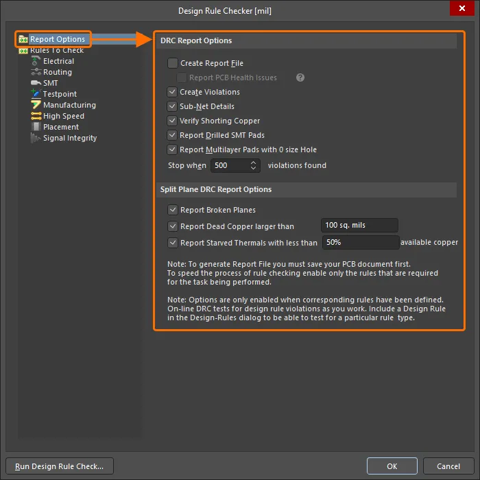
-
Click the Report Options entry in the tree on the left-hand side of the dialog to configure additional options that are available when running a Batch DRC.
-
Click the Rules to Check entry or an entry for a specific rule category to load the dialog with a list of rule types and enable each rule type for Online and/or Batch DRC as required:
-
Online DRC – the check will be performed in real-time as you design.
-
Batch DRC – the check will be performed as a batch process by clicking the Run Design Rule Check button in the dialog, with results listed in the Messages panel and an optional generated report.
-


When running an Online or Batch DRC, detected rule violations will be indicated in the design space (using the custom violation graphics and/or violation overlay). Some examples of violations in the design space are shown below:

Tracks offending a Width rule. The violation is indicated by both custom violation graphics and violation overlay.

A track offending a Net Antennae rule. The violation is indicated by custom violation graphics.
You can configure how violations of different rule types are displayed in the design space using the PCB Editor – DRC Violations Display page of the Preferences dialog.
Based on information on how much a violation has failed, you can decide how best to resolve the violation. For example, if the minimum solder mask sliver constraint is set to 0.25 mm and the actual sliver is 0.24 mm, then the situation is not that bad and you may be able to adjust the constraint to accept this value. But if the actual sliver value is 0.02, then that is probably not a situation that can be resolved by adjusting the constraint.
-
The detail is included in the Messages panel. The actual value is detailed along with the specified value (for example, 0.017mm < 0.254mm).
-
You can also right-click on a violation and open the Violations sub-menu to examine what constraint is being violated and the violation conditions (
 ).
).
-
The PCB editor also includes handy measurement tools that allow you measuring distance between two points, measuring selected objects (length of selected tracks and arcs), and measuring distance between two primitives. Refer to the Measuring Distances on a PCB page to learn more.
The PCB Rules And Violations panel is an excellent feature for locating and understanding violation conditions. It will default to show [All Rules] in the Rule Classes list. Once you have identified a rule type of interest, select that specific rule class so that only those violations are shown at the bottom of the panel. The panel details the violation type, the measured value, the constraint, and the objects that are in violation. Detected rule violations for the selected rule class or specific rule are also listed in the Violations region of the panel. Click a violation entry to highlight the violation in the design space, according to the setting at the top of the panel: Mask/Dim/Normal, Select, Zoom. Double-click on a violation to open the Violation Details dialog.

DRC can also be run for all rules, rules of a specific type, or a specific rule by right-clicking the associated entry in the PCB Rules And Violations panel and selecting the Run DRC command.

Run DRC right from the PCB Rules And Violations panel. Running DRC for all defined Clearance rules is shown here.
Learn more about DRC: Design Rule Check (DRC).