Advanced PCB Design Technologies in Altium Designer
Today's compact electronic products are delivered in compact and unusually shaped enclosures. Often powered by batteries they are light-weight and portable, requiring lower signal voltages and power consumption. And these compact designs use the latest device technologies with fast switching speeds, speeds so fast that the routing is no longer a set of simple copper paths that carry a current and expresses a voltage, now the routes are an array of transmission lines - turning the routing process into an engineering analysis and design challenge in its own right.
All of this brings many new challenges for the design and implementation phase of electronic product development. Various design technologies have emerged to help, many of which are available in Altium Designer.
Wire Bonding
The primary objective of wire bonding is to establish a secure and low-resistance electrical connection between a semiconductor chip and its package or between different chips within a multi-chip module. This process involves bonding a fine wire, typically made of gold, aluminum, or copper, from the bond pad on the chip to a corresponding pad on the package substrate or another chip.
Wire bonding transmits power and signals between substrates and chips. It is the basic technology in which an electrical connection between the chip contact surfaces (pads) and the chip carrier or substrate is established by the micro-welding of micro-wires. it is generally considered the most cost-effective and flexible interconnect technology and is used to assemble most semiconductor packages.
Altium Designer supports the design of hybrid boards with chip-on-board (CoB) technology using Wire Bonding.
► Learn more about Wire Bonding
Direct Layout & Routing on a 3D Substrate
3D-MID technology combines electrical circuits with three-dimensional mechanical parts. This fusion of functionality opens up a world of possibilities within a vast range of application areas.
Historically, designers of 3D-MIDs have generally been restricted to MCAD packages due to the lack of suitable ECAD tools. There are many problems inherent to this way of working, not least is the absence of any electrical intelligence to drive the circuit layout and the difficulties associated with projecting 2D manually-drawn sketches onto 3D surfaces.
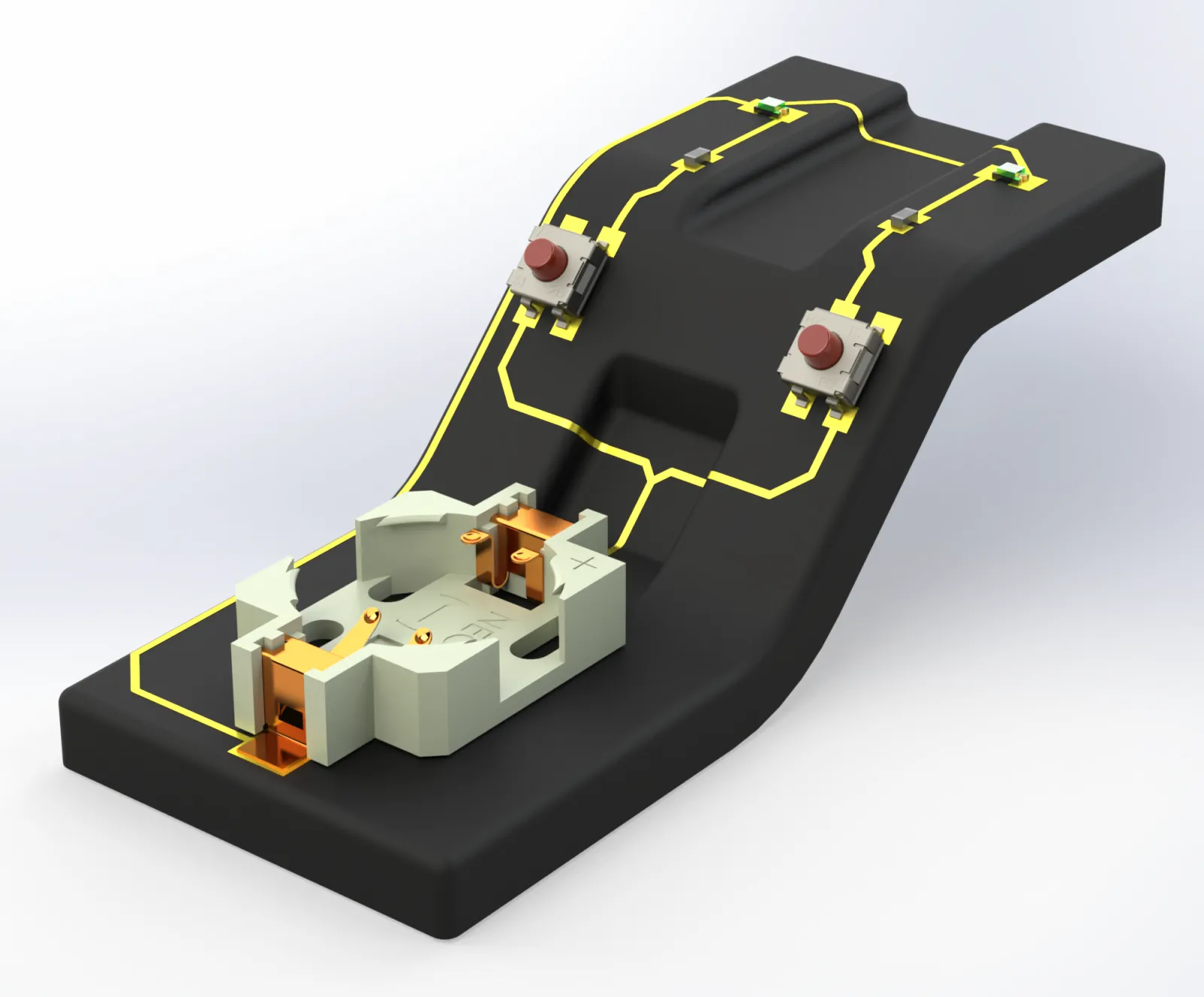
The new 3D routing technology allows you to place standard surface mount components onto a 3D shape and route traces along the surface of the shape to complete the layout.
The completed design can then be exported in the file format required by the Laser Direct Structuring (LDS) manufacturing process.
► Learn more about Direct Layout & Routing on a 3D Substrate
Printed Electronics
An exciting evolution in the design and development of electronic products is the ability to print the electronic circuit directly onto a substrate, such as a plastic molding that becomes a part of the product.
Printed electronics will become a pivotal technology, allowing the integration of electronics into new markets. Printed electronics allow an intimate connection between the circuit and the product. From a flexible sensor that attaches directly to the body, through to a multi-sensor, finger tip-shaped molding that allows a robotic hand to hold a soft plastic cup as liquid is poured into it, printed electronics will allow innovative new solutions to be developed across many market segments.
► Learn more about Printed Electronics
Designing with Embedded Components
The ever-increasing demand for smaller and more integrated electronic products, combined with the higher frequencies of the signals within these devices, drives the ongoing research into better ways to fabricate and assemble a circuit.
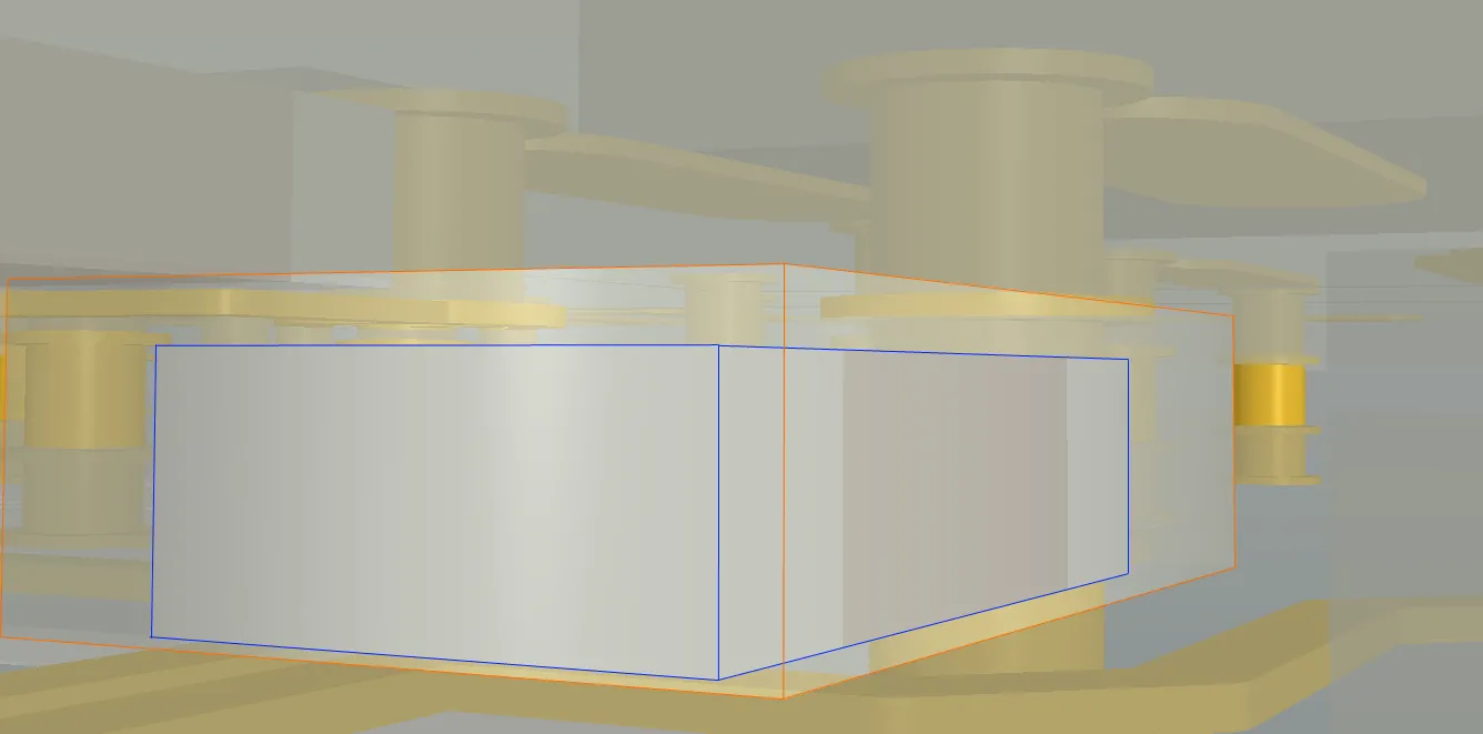
One technique that delivers both higher density and improved support for higher signal frequencies, is to embed components within the layers of the circuit structure. For example, embedding discrete components directly under an integrated circuit can result in: shorter signal lengths; reduced resistance and parasitic inductance, leading to lower noise and EMI; and improved integrity of the circuit signals. These improvements deliver smaller and more reliable products, supporting faster signal speeds and higher bandwidths. Combined with the on-going improvements being achieved in fabrication processes and technologies, they can also lead to a reduction in the product size, and lower fabrication and board level assembly costs.
Embedding components places a number of unusual demands on each stage of the process: from design, to fabrication, to assembly, to testing and maintenance of the finished product.
► Learn more about Embedded Components
Designing with Touch Controls

Touch sensitive electronics are on the forefront of technology. As the user interface becomes more important to the success of your product, clean and modern controls are now considered essential.
Adding a touch sensor to your electronic product is a process that starts at the beginning of a design, and extends into the board design process. Altium Designer's touch sensor support allows you do to easily integrate touch sensors into your design workflow.
Altium Designer's touch control support includes:
- Configurable touch sensor libraries that let you set the controls and parameters of your device from the start.
- Automatically generate the complex land patterns and footprints required for touch sensors.
- Model and verify your designs in Native 3D to make sure they are aligned and fit correctly.
- Atmel® QTouch® and QMatrix® libraries; Cypress® Capsense® libraries; & Microchip® mTouch® libraries
► Learn more about Designing with Touch Controls


