If your designs often include common 'sections' of circuitry, Altium Designer provides a simple and easy way to save and reuse sections of design circuitry, both Workspace-based and local, file-based. Such sections can be added to any PCB design without having to start from scratch each time. This is a great feature for those often-used fragments and smaller sections of circuitry that you want to reuse. The system lets you save any selection of:
-
Circuitry on a single schematic sheet (a schematic snippet).
-
Circuitry in a PCB design, including the components and the routing (a PCB snippet).
When connected to a Workspace, you can create a single entity – a Reuse Block – that can contain both schematic circuitry and its physical representation for the PCB. When such a reuse block is placed on a schematic sheet, its physical representation will be placed automatically in the PCB document during the ECO process.
The Design Reuse panel is the command center for creating, managing, and using reuse blocks and snippets—both Workspace-based and local file-based.

The Design Reuse panel
The panel can be accessed in the following ways:
-
Click the Panels button at the bottom right of the design space then click Design Reuse.
-
Select View » Panels » Design Reuse from the main menus.
-
Select Place » Reuse Block from the main menus.
The panel's top drop-down menu lists all available folders currently existing in your connected Workspace, which contain reuse blocks and Workspace-based snippets. The number next to each folder name shows how many design reuse blocks and snippets this folder and its sub-folders contain. Select a folder in the drop-down to present the reuse blocks and snippets this folder and its sub-folders contain in the main section of the panel. Select the entry of your connected Workspace in the drop-down to present all available reuse blocks and snippets.
The Workspace folder structure can be defined from within Altium Designer using the
Explorer panel.
Use filter buttons in the  icon pop-up to show/hide the content of specific types (Reuse Blocks, Schematic Snippets, PCB Snippets) in the panel. Use the Sort By control to select a preferred sorting option.
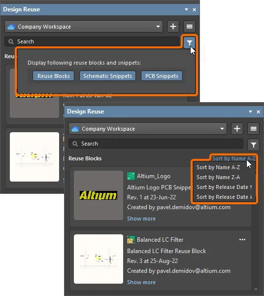
Use filtering and sorting options to configure the content display in the panel
To search for available reuse blocks and snippets in the selected folder by their name or description, enter a phrase in the Search field to effectively filter and narrow the listing to your specific needs.
Each reuse block and snippet is presented in the main panel's section by the tile that contains the following data:
-
Preview image – can be clicked to switch between normal and full-scale states. For a reuse block, use the
 button to switch between its PCB and schematic model previews;
-
The type icon –
 for a reuse block,
  for a schematic snippet,
  for a PCB snippet;
-
Name and description (if defined);
-
The latest revision's ID, creation date, and author of a reuse block or a Workspace schematic/PCB snippet.

Information about and controls for a reuse block or snippet are presented in a tile within the panel.
Creating a Reuse Block
Copy Link
Copied
A new reuse block can be created in the following ways:
-
Select the command for creating a new reuse block:
-
From the Design Reuse panel, by clicking the  button at the top of the panel.
-
By using the File » New » Reuse Block command from the main menu.
-
From the Explorer panel, by clicking the  button located at the top-right of the panel when a folder of the
 Design Reuse Blocks type is being browsed.
-
A temporary editable PCB project-like structure of the reuse block will be opened in the Projects panel (under an entry for the Workspace you are currently connected to), and the temporary schematic editor will be opened in the main design window, ready for defining the schematic model of the reuse block. Use the standard placement commands and techniques to define the schematic model of the reuse block.
-
When done, use the Design » Update PCB Document command and the ECO process to transfer the captured schematic to the PCB model of the reuse block, then apply the changes needed to that model (defining component locations, routing, etc.).
Multiple PCB models can be added to the reuse block being defined. To do this, use the Add New to Project » PCB command from the right-click menu of the reuse block's entry in the Projects panel.

Use the Rename command from the right-click menu of the added PCB model's entry in the Projects panel to define a meaningful name for it. Use a Design » Update command from the schematic editor main menu to update the required PCB document.
When both schematic and PCB models of the reuse block are defined, save the reuse block to the Workspace using the Save to Server command from the context menu of the reuse block's entry in the Projects panel or the Save to Server control to the right of the entry.
Because reuse blocks are stored in the connected Workspace, they should use components from that Workspace. That way, you get the full benefit of the content system the Workspace provides.
-
Both schematic and PCB models of the reuse block must contain at least one component in order to be saved to the Workspace.
-
If the reuse block's schematic and PCB documents are not synchronized (differences between the schematic and PCB documents are detected), the warning dialog will be shown when trying to save the reuse block to the Workspace. You can cancel saving to return to the reuse block and address the differences or proceed with saving.
-
The New Reuse Block dialog will appear, in which you can define Name, Description, and the Workspace Folder into which the new reuse block will be saved.
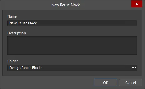
The New Reuse Block dialog
Options and Controls of the New Reuse Block Dialog
Copy Link
Copied
-
Name – enter the name of the new reuse block or snippet.
-
Description – use this field to enter a meaningful description of what is represented by this reuse block or snippet.
-
Folder – the Workspace folder in which this reuse block or snippet will be stored. Click
 to open the Choose Folder dialog to select or create a different folder.
-
After clicking OK, the reuse block will be saved to the Workspace and its temporary structure will be closed.
A saved reuse block can then be found in the Design Reuse panel when the folder it has been saved into (or the entry of your connected Workspace) is selected in the top drop-down. Using the Refresh command from the  button menu may be required for the new reuse block to appear in the panel.
Renaming a Reuse Block
After a Reuse Block is created, it can be renamed to a more suitable title if desired. To rename a Reuse Block, use the Rename command, which can be accessed from the  sub-menu and the right-click context menu of the Design Reuse panel. In the Rename Reuse Block dialog that opens, enter the new title, then click OK. The name of the Reuse Block is now the desired name, as shown in the following images.

Creating a Snippet
Copy Link
Copied
A new schematic or PCB snippet can be quickly created from an existing circuitry on a schematic sheet or a PCB document:
-
Select the required circuitry on the schematic or PCB editor.
-
Right-click and choose the Snippets » Create Snippet from selected objects from the context menu or select the Tools » Convert » Create Snippet from selected objects command from the main menus.
-
The New Schematic Snippet or New PCB Snippet dialog will appear, in which you can define the Name, Description, saving destination (a Workspace or a local folder), and the folder into which the new snippet will be saved.
When saving a snippet to a local folder, click the  button at the right of the Path field in the dialog to access the Choose Snippet Folder dialog, which allows you to select an existing local snippet folder into which the snippet will be saved, or create a new sub-folder within an existing local snippet folder.
-
After clicking OK, the snippet will be saved.
A saved snippet can then be found in the Design Reuse panel when the entry of your connected Workspace (or the folder it has been saved into) is selected in the top drop-down.
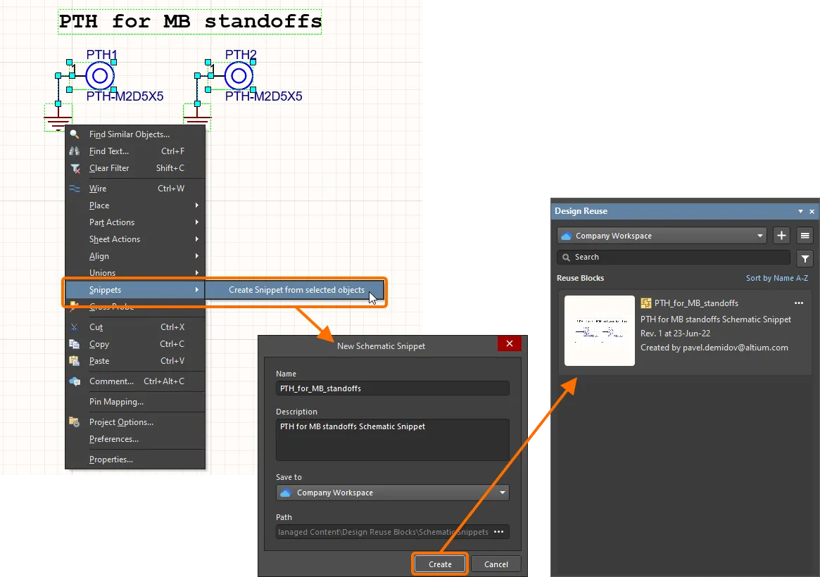
A snippet can be created from a set of selected objects. Shown here is creating a schematic snippet. Hover the cursor over the image to see creation of a PCB snippet.
Using the Refresh command from the panel's  button menu may be required for the new reuse block to appear in the panel.
For access to local snippets from the
Design Reuse panel, the
Local Snippets option must be enabled in the

menu.
A Workspace-based snippet can also be created from an existing local snippet by clicking the  button within the snippet's tile (or by right-clicking anywhere on the tile) and selecting the Save to Server command from the menu. In the New Schematic Snippet or New PCB Snippet dialog that appears, define the Name, Description, and the Workspace Folder into which the snippet will be saved.
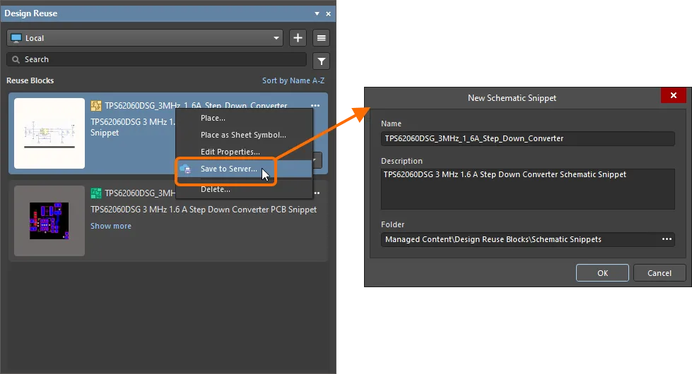
A local snippet can be saved to the connected Workspace using the Save to Server command.
Workspace snippets should use components from that Workspace. That way, you get the full benefit of the content system the Workspace provides.
Local Snippet Organization
The Design Reuse panel allows local snippets to be organized into snippet folders so that related snippets can be grouped together, making it easier for you to find them. Snippets folders are existing Windows folders that cannot be created from within the Design Reuse panel. Instead, they are 'opened' or 'closed' when browsing the local snippets they contain. These folders can only be created directly on your hard disk or network outside of Altium Designer.
Snippets folders can be opened and closed from the Available Snippets Folders dialog accessed by clicking the  button at the top right of the Design Reuse panel and selecting the Snippet Folders command from the menu. Click Open Folder to browse to the required folder on your hard disk or network. The selected folder will be added to the list in the dialog and subsequently appear in the drop-down at the top of the Design Reuse panel.

To remove a snippets folder from the list (essentially closing it from a browsing perspective), select the folder in the list, then click Remove Folder. Use the Move Up and Move Down buttons to change the order in which the local snippets will be presented in the Design Reuse panel when the Local entry is selected in the panel's drop-down.
Placing Reuse Blocks and Snippets
Copy Link
Copied
To place a reuse block or a snippet in a design, click within its tile and click the  button, click the
  button within its tile, or right-click anywhere on the tile and select one of the following commands:
-
Place – select to place the reuse block or snippet directly on the active schematic or PCB document.
-
Place as Sheet Symbol – when a schematic document is active, select to place the reuse block or schematic snippet as a Sheet Symbol on the schematic sheet. The content of the reuse block or schematic snippet will be placed on an automatically created child schematic sheet referenced by the placed Sheet Symbol.

Place a reuse block or snippet using the Place button menu within its tile in the panel. Selecting the Place command where the reuse block / schematic snippet is placed on the active schematic sheet is shown here. Hover the cursor over the image to view selecting the Place as Sheet Symbol command where the reuse block / schematic snippet is placed on the child sheet referenced by the placed Sheet Symbol.
Click the Show more control within the reuse block's tile to present the PCB section that contains the list of the reuse block's PCB models. Select the required PCB model in the list, and the reuse block will be placed with this model. The selected PCB model is shown in the preview area of the reuse block's tile when PCB is selected for preview.
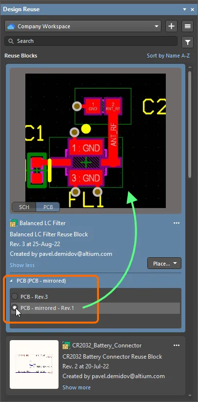
Select a PCB model to be placed with the reuse block to present its preview.
After placing the schematic model of a reuse block, its PCB model can be placed in the PCB document through the ECO process. From the schematic editor, use the Design » Update PCB Document command from the main menus, then validate and execute changes using the Engineering Change Order dialog. The PCB model will be placed in the PCB document as a union and it can be managed from the Unions mode of the PCB panel.
When a selected schematic or PCB component is part of a reuse block placed in the design, you can inspect its properties by clicking the Reuse Block link provided in the Properties panel. The properties of the component's parent reuse block will be presented in the panel. To return to the properties of the initially selected component, use the Component link.
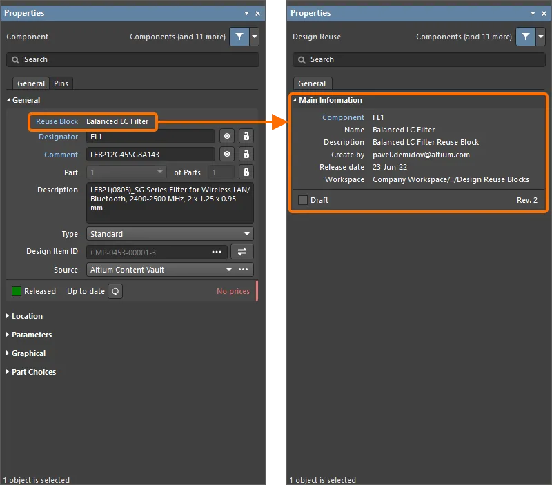
Access the reuse block properties from a component that is a part of this reuse block. The images above display accessing the properties from a schematic component. Hover the cursor over the image to see access from a PCB component.
For a reuse block, its schematic or PCB model will be used when using the place command, depending on the type of document that is active when running the command.
For a snippet, ensure you have the correct target document open as the active document before placing the snippet. The place command will only be functional if the snippet can correctly be placed on that document, i.e. the snippet type and document type must be the same.
Editing Reuse Blocks and Snippets
Copy Link
Copied
To edit a Workspace-based reuse block or snippet, click the  button within its tile (or right-click anywhere on the tile) and select the Edit command from the menu.
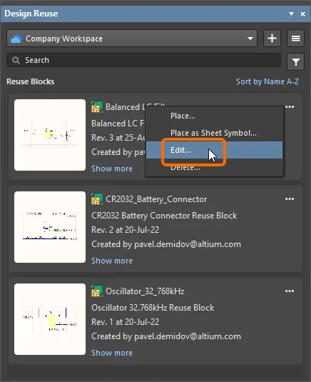
Open a Workspace-based reuse block or snippet for editing using the Edit command from within its tile in the panel.
The temporary editor will open, with the document (containing the source reuse block/snippet) contained in the latest revision of the Workspace Item, opened for editing. Make changes as required, then save the document into the next revision of the reuse block/snippet using the File » Save to Server command from the main menu or the Save to Server command from the reuse block/snippet entry's right-click menu in the Projects panel.
The properties (Name, Description, and Path) of a local snippet can be edited through the Snippet Properties dialog that is accessed by clicking the  button within the local snippet's tile (or right-clicking anywhere on the tile) and selecting the Edit Properties command from the menu.

Edit properties of a local snippet using the Snippet Properties dialog accessed from the Design Reuse panel.
Deleting Reuse Blocks and Snippets
Copy Link
Copied
To delete a reuse block or snippet, click the  button within the snippet's tile (or right-click anywhere on the tile) and select the Save to Server command from the menu.
-
For a Workspace-based reuse block or snippet, the Delete Items dialog will appear, in which to confirm the deletion. The action is actually a 'soft delete', whereby the reuse block or snippet will be moved into the Trash area of the Workspace. The Trash is essentially a recycle bin into which any content within your Workspace can be moved (through a soft delete action). It is isolated from the rest of the Workspace. For a reuse block, you can also opt to delete the reuse block's related content (e.g., schematic and PCB snippets).
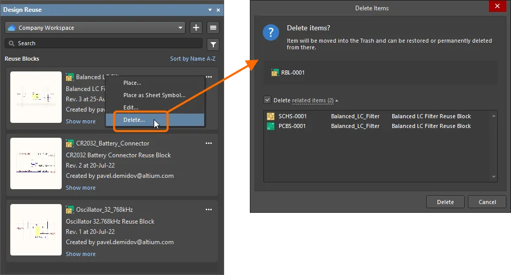
Soft-delete a reuse block or snippet using the Delete command from within its tile in the panel.
-
For a local snippet, the Confirm dialog will appear to confirm the deletion. The action will remove the snippet files from your hard drive.
