Parent page: Tutorial - A Complete Design Walkthrough with Altium Designer
Positioning the Components on the PCB
There is a saying that PCB design is 90% placement and 10% routing. While you could argue about the percentage of each, it is generally accepted that good component placement is critical for good board design. Keep in mind that you may need to also tune the placement as you route.
Component Positioning and Placement options
When you click and hold on a component to move it, if the Snap to Center option is on, then the component will be held by its reference point. The reference point is the 0,0 coordinate of the component as it was built in the library editor.
The Smart Component Snap option allows you to override this snap to center behavior and snap to the nearest component pad instead, which is handy when you need to position a specific pad in a specific location.

Enable Snap To Center to always hold the component by its reference point. Smart Component Snap is helpful when you need to align by a specific pad.
Setting the component positioning options
-
Click the
 icon located at the top-right of the application window to open the Preferences dialog.
-
Open the PCB Editor – General page of the Preferences dialog. In the Editing Options section, make sure the Snap To Center option is enabled. This ensures that when you "grab" a component to position it, the cursor will hold the component by its reference point.
-
Note the Smart Component Snap option. If this is enabled, you can force the software to snap to a pad center instead of the reference point by clicking and holding closer to the required pad than the component's reference point. This is very handy if you require a specific pad to be on a specific grid point. It can work against you if you are working with small surface mount components though, as it can make it harder to "grab" them by their reference point.
-
Click OK to save changes and close the Preferences dialog.
Positioning Components
You can now position the components in suitable locations on the board.
To move a component either:
-
Click, Hold&Drag to move the component to the required location, rotate it with the Spacebar, then release the mouse button to place it, or
-
Run the Edit » Move » Component command, then single click to pick up a component, move it to the required location, rotate it if required, then click once to place it. When you are finished, right-click to drop out of the Move Component command.
The connection lines are automatically re-optimized as you move a component. Use them to help orient and position the components to reduce the number of connection line cross-overs.
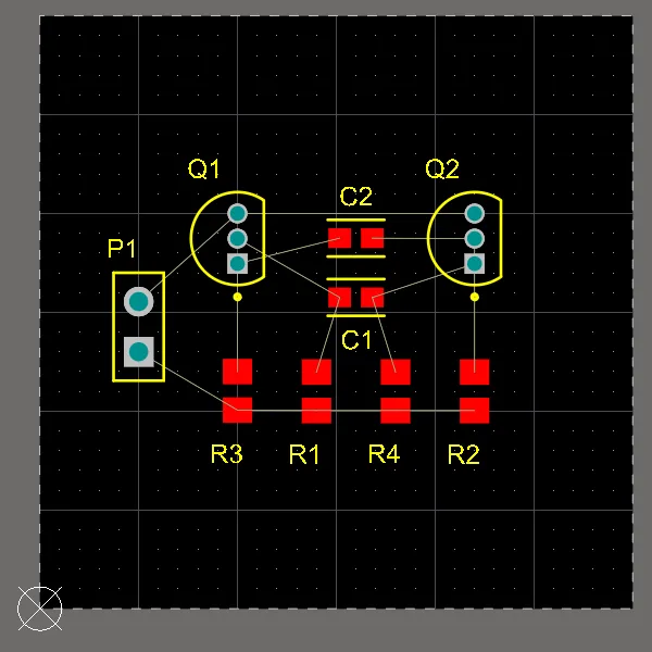
Components positioned on the board.
Positioning the components
-
Zoom to display the board and the component. One way to do this is to zoom out (PgDn) so the board and the components are all visible then choose View » View Area, then click to define the top left and bottom right of the exact area you want to view.
-
The components will be positioned on the current Snap grid. For a simple design such as this, there are no specific design requirements that dictate what placement grid should be used. As the designer, you decide what a suitable placement grid would be. To simplify the process of positioning the components, you can work with a coarse placement grid, for example, 1mm. Check the Status Bar to confirm that the Snap Grid is set to
1mm; press Ctrl+Shift+G to change the grid if required.
-
The components in the tutorial can be placed as shown in the image above. To place connector
P1, position the cursor over the middle of the outline of the connector and use Click, Hold&Drag. The cursor will change to a crosshair and jump to the reference point for the part (or the center of the nearest pad if you have enabled the Smart Component Snap option). While continuing to hold down the mouse button, move the mouse to drag the component.
-
Press the Spacebar to rotate the component if required, and position the footprint towards the left-hand side of the board as shown in the figure above.
-
When the connector component is in position, release the mouse button to drop it into place. Note how the connection lines drag with the component.
-
Reposition the remaining components, using the figure above as a guide. Use the Spacebar to rotate components (in increments of 90º counterclockwise) as you drag them so that the connection lines are as shown in the figure.
-
Component text can be repositioned in a similar fashion; click-and-drag the text and press the Spacebar to rotate it.
-
The PCB editor also includes interactive placement tools. These can be used to ensure that the four resistors are correctly aligned and spaced.
-
Holding the Shift key, click on each of the four resistors to select them, or click and drag the selection box around all four of them. A shaded selection box will display around each of the selected components. The Selection color is defined in the System Colors section of the View Configuration panel.
-
Right-click on any of the selected components and choose Align » Align to open the Align Objects dialog.
-
Select Space Equally in the Horizontal section and Bottom in the Vertical section, then click OK to apply these changes. The four resistors are now aligned (with the lowest component) and equally spaced.


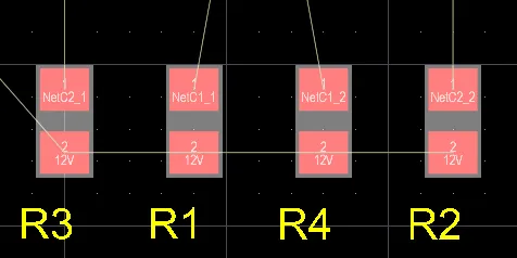
Select then align and space the resistors.
-
Click elsewhere in the design space to deselect all the resistors. If required, you can also align the capacitors and transistors, although this might not be required since you have a coarse Snap grid at the moment.
-
Reposition component designators if needed – click, hold and drag a designator, or use the Autoposition option in the Properties panel when designator(s) are selected in the design space.
-
Save the PCB file locally.
-
Selected objects can also be moved using the keyboard rather than the mouse. To do this, hold Ctrl, then each time you press an Arrow key, the selection will move 1 grid step in the direction of that arrow. Include the Shift key to move selected objects in 10x Snap Grid steps.
-
As you move a component with the mouse, you can constrain it to an axis by holding the Alt key. The component will attempt to hold the same horizontal axis (if moving horizontally) or vertical axis (if moving vertically); move it further from the axis to override this behavior or release the Alt key.
With the components positioned, it's time to do some routing!
Interactively Routing the Board
Main page: Interactive Routing
Routing is the process of laying tracks and vias on the board to connect the component pins. The PCB editor makes this job easy by providing sophisticated interactive routing tools, as well as ActiveRoute, which optimally routes selected connections with the click of a button.
In this section of the tutorial, you will manually route the entire board single-sided, with all tracks on the top layer. The Interactive Routing tools help maximize routing efficiency and flexibility in an intuitive way, including cursor guidance for track placement, single-click routing of the connection, pushing obstacles, automatically following existing connections, all in accordance with applicable design rules.
Preparing for Interactive Routing
Preferences page: PCB Editor – Interactive Routing
Before starting to route, configure the Interactive Routing options in the PCB Editor – Interactive Routing page of the Preferences dialog.
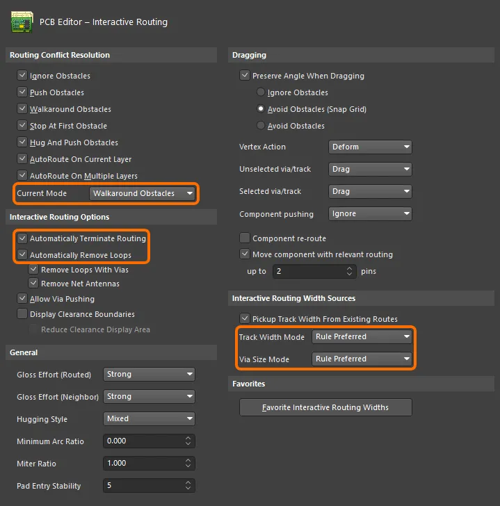
Configure the interactive routing options.
Preparing for interactive routing
-
Open the PCB Editor – Interactive Routing page of the Preferences dialog.
-
Set the Routing Conflict Resolution Current Mode to
Walkaround Obstacles. As you are routing, you can cycle through the enabled modes by pressing Shift+R.
-
In the Interactive Routing Options section of the page, confirm that the Automatically Terminate Routing and the Automatically Remove Loops options are enabled. The first option releases the cursor from the current route when you click on the destination pad to finish that route. The second option allows you to change existing routing by routing an alternate path – you route a new path until it meets the old path (creating a loop), then right-click to indicate it is complete. The software then automatically removes the old, redundant part of the routing. This feature will be explored later in the tutorial.
-
Confirm that the Track Width Mode / Via Size Mode options are both set to Rule Preferred.
-
Click OK to save changes and close the Preferences dialog.
-
Press Ctrl+Shift+G to open the Snap Grid dialog and set the Snap Grid to
0.25mm.
Time to Route
-
Interactive routing is launched by clicking the Route button
 , or by selecting the routing command (Route » Interactive Routing, shortcut: Ctrl+W).
-
Since the components are mostly surface mount and the design is simple, the board can be routed on the top layer. As you place tracks on the top layer of the board, use the ratsnest (connection lines) to guide you.
-
Tracks on a PCB are made from a series of straight segments. Each time there is a change of direction, a new track segment begins. Also, by default, the PCB editor constrains tracks to a vertical, horizontal, or 45° orientation, allowing you to easily produce professional results. This behavior can be customized to suit your needs, but for this tutorial, you can use the defaults.
-
When the routing reaches the target pad, the software will automatically release that connection and you will remain in Interactive Routing mode, ready to click on the next connection line.
A simple animation showing the board being routed. Many of the connections are finished using Ctrl+Click to autocomplete.
Interactively routing the board
-
Check which layers are currently visible by looking at the Layer Tabs at the bottom of the design space. If the Bottom Layer is not visible, press the L shortcut to open the View Configuration panel, and enable the Bottom Layer.
-
Click on the Top Layer tab at the bottom of the design space to make it the current, or active layer, ready to route on.
-
It is often easier to route in single layer mode; press Shift+S to cycle through the enabled single layer modes.
-
Click
 on the Active Bar (or the Ctrl+W shortcut), or select Interactive Routing from the Route menu, or right-click and choose Interactive Routing from the context menu. The cursor will change to a crosshair, indicating you are in interactive routing mode.
-
Position the cursor over the lower pad on connector P1. As you move the cursor close to the pad, it will automatically snap to the center of the pad. This is the Objects for snapping feature pulling the cursor to the enabled hotspot of the nearest electrical object (configure the Snap Distance and the Objects for snapping in the Snap Options section of the Properties panel). Sometimes the Objects for snapping feature pulls the cursor when you don't want it to. In this situation, press the Ctrl key to temporarily inhibit snapping. Alternatively, use the Shift+E shortcut to cycle the Hotspot Snap mode through the three possible states – Hotspot Snap (All Layers) / Hotspot Snap (only snaps on the current layer) / Off (nothing displayed). The current mode is displayed on the Status Bar.
► Learn more about Working with the PCB Grids System, including object snapping.
-
Left-Click or press Enter to anchor the first point of the track.
-
Move the cursor toward the bottom pad of the resistor R3, and click to place a vertical segment. Note how track segments are displayed in different ways (as shown in the image below). During routing, the segments are shown as:
-
Solid – the segment has been placed.
-
Hatched – hatched segments are proposed but uncommitted; they will be placed when you left-click.
-
Hollow – this is referred to as the look-ahead segment, it allows you to work out where the last proposed segment should end. This segment is not placed when you click unless the next click will complete the route. In this situation, the Automatically Terminate Routing option kicks in and overrides the default look-ahead behavior. The look-ahead mode can be toggled on/off using the 1 shortcut during routing.


Solid segments are placed, hatched are proposed but not committed, hollow is the look-ahead segment. Press the 1 shortcut to toggle look-ahead on/off.
-
Manually route by left-clicking to commit track segments, finishing on the lower pad of R2. Note how each mouse click places the hatched segment(s). For the connection that you are currently routing, press Backspace to rip up the last-placed segment.
-
Rather than routing all the way to the target pad, you can also press Ctrl+Click to use the Auto-Complete function and instruct the software to attempt to route the entire connection. Auto-complete behaves in the following ways:
-
It takes the shortest path, which may not the best path as you need to always consider paths for other connections yet to be routed. If you are in Push mode (shown on the Status Bar when routing), Auto-complete can push existing routes to reach the target.
-
On longer connections, the Auto-Complete path may not always be available as the routing path is mapped section by section, and complete mapping between source and target pads may not be possible.
-
You can also Auto-complete (Ctrl+Click) directly on a pad or connection line.
-
Continue to route all the connections on the board. The animation above shows the board being interactively routed.
In the animation above, there is a route from the upper pad of R1 to the middle pin of Q1, that is placed on the bottom layer. Depending on the brand of surface mount resistor that you chose, it may be possible to place this route so that it passes between the pads of R3. For example, Panasonic resistors are slightly smaller, it will not be possible to route a track between the pads of their footprint. In this situation, you will need to route one connection on the bottom layer to complete the routing. To switch layers and place a via while routing, use the * key on the numeric keypad, or the Ctrl+Shift+Mouse Wheel shortcut combination. On the other hand, Yageo and Vishay Dale resistors are slightly larger and the pads of their footprint have sufficient space between them to route using the width and clearance configured in this design.
-
There is no single solution to routing a board, so it is inevitable that you will want to change the routing. The PCB editor includes features and tools to help with this; they are discussed in the following sections and are also demonstrated in the animation shown above.
-
Save the design locally when you are finished routing.
| Shortcut Icon |
Action |
 |
Keyboard key combination, press Ctrl+W to start Interactive Routing. |
 |
Key + mouse combination, press Ctrl+Click to auto-complete the current connection. Only functions during Interactive Routing. |
 |
Click, Hold&Drag, use this to drag an existing route. It can be used when no other command is being run. |
Interactive Routing Modes
The PCB editor's Interactive Routing engine supports a number of different modes, with each mode helping you deal with particular situations. Press the Shift+R shortcut to cycle through these modes as you interactively route. Note that the current mode is displayed on the Status Bar and in the Heads-Up display.
Available interactive routing modes
-
Ignore Obstacles – this mode lets you place tracks anywhere, including over existing objects, displaying but allowing potential violations.
-
Stop at first Obstacle – in this mode, the routing is essentially manual, i.e. as soon as an obstacle is encountered, the track segment will be clipped to avoid a violation.
-
Walkaround Obstacles – this mode will attempt to find a routing path around existing obstacles without attempting to move them.
-
Hug & Push Obstacles – this mode is a combination of Walkaround and Push. It will hug as it performs a Walkaround of obstacles, however, it will also attempt to Push against fixed obstacles when there is insufficient clearance to continue using Walkaround.
-
Push Obstacles – this mode will attempt to move objects (tracks and vias), which are capable of being repositioned without violation to accommodate the new routing.
-
Autoroute on Current Layer – this mode brings basic autorouting functionality to interactive routing. It can automatically select between walkaround and push based on heuristics that consider push distance versus walk distance and route length. Like an autorouter, this mode can deliver better results on a complex, busy board than on a simple, unrouted board.
-
Autoroute on Multiple Layers – this mode also brings basic autorouting functionality to interactive routing, it can also automatically select between walkaround and push based on heuristics that consider push distance versus walk distance and route length. This mode can also place a via and consider using other routing layers. Like an autorouter, this mode can deliver better results on a complex, busy board than on a simple, unrouted board.
Interactive Routing modes that are not required can be disabled in the PCB Editor – Interactive Editing page of the Preferences dialog.
Routing Tips and Tricks
The PCB editor includes a range of features to help make the interactive routing process more efficient, including in-command shortcuts that you use during routing, detailed feedback via the Status Bar and the Heads Up display, and the ability to display clearance boundaries as you route.
Routing Shortcuts
Useful shortcuts during routing:
| Keystroke |
Behavior |
| Shift+F1 |
Pop up a menu of interactive shortcuts – most settings can be changed on the fly by pressing the appropriate shortcut or selecting from the menu. |
| * or Ctrl+Shift+Mouse Wheel |
Switch to the next available signal layer. A via is automatically added in accordance with the applicable Routing Via Style design rule. Learn more about changing layers and adding a via as you route. |
| Tab |
Open the Interactive Routing mode of the Properties panel, where you can change the routing settings. |
| Shift+R |
Cycle through the enabled routing conflict resolution modes. Configure your preferred modes in the PCB Editor – Interactive Routing preferences page. |
| Shift+S |
Cycle through the available Single Layer Modes. This feature is ideal when there are many objects on multiple layers. Configure the available modes in the PCB Editor – Board Insight Display page. |
| Spacebar |
Toggle the current corner direction. |
| Shift+Spacebar |
Cycle through the various track corner modes. The styles are any angle, 45°, 45° with arc, 90°, and 90° with arc. There is an option to limit this to 45° and 90° on the PCB Editor – Interactive Routing preferences page. |
| Ctrl+Shift+G |
Cycle through the three Gloss strength (Gloss Effort (Routed)) settings. The current setting is displayed in the Heads Up display and on the Status Bar. |
| Ctrl+Click |
Auto-complete the connection being routed. Auto-complete will not succeed if there are unresolvable conflicts with obstacles. |
| 1 |
Toggle the Look-ahead mode on/off. |
| 3 |
Cycle through the routing width choices: Rule Minimum / Rule Preferred / Rule Maximum / User Choice. Learn more about changing the width as you route. |
| 4 |
Cycle through the routing via style choices: Rule Minimum / Rule Preferred / Rule Maximum / User Choice. Learn more about changing the via style as you route. |
| 6 |
Cycle through available Via Types. |
| Shift+E |
Cycle through the three object Hotspot Snap modes: off / on for current layer / on for all layers. |
| Ctrl |
Temporarily suspend object snapping feature while routing. |
| End |
Redraw the screen. |
| PgUp / PgDn |
Zoom in / out, centered around the current cursor position. Alternatively, use the standard Windows mouse wheel zoom and pan shortcuts. |
| Backspace |
Remove the last-committed track segment. |
| Right-Click or Esc |
Drop the current connection and remain in Interactive Routing mode. |
Feedback During Interactive Routing
It is essential to know the name of the net or the current width setting as you route a net. This information, along with a wealth of other useful details, is available in the Heads-Up display and on the Status Bar during routing. An excellent feature to help visualize the amount of space available for routing is the ability to display clearance boundaries around all other net-objects. The image below demonstrates this; as the 12V net is being routed, all other net objects display a clearance boundary defined by the applicable Electrical Clearance Constraint (which was defined earlier in the tutorial). It is not possible to cross this boundary during routing.
-
Press Shift+H to toggle the Heads-Up display off and on. Configure the display content, color, and fonts in the PCB Editor – Board Insight Modes page of the Preferences dialog.
-
Press Ctrl+W to toggle the clearance boundaries off and on.

Heads-Up display and Status Bar information during interactive routing:
-
Current design space location and Snap Grid setting
-
Object Hotspot Snapping: off / on for current layer / on for all layers
-
Current track corner mode
-
Current Interactive Routing Mode
-
Source of routing Width
-
Source of routing Via Style
-
Name of Via Type that will be used
-
Current Gloss strength
-
Name of Net
-
Overall route length
-
Dimensions of routing segment being placed
Modifying and Rerouting Existing Routes
To modify an existing route, there are two approaches, either: reroute, or re-arrange.
Reroute an existing Route
-
There is no need to un-route a connection to redefine its path. You can click the Route button
 and start routing the new path.
-
The Loop Removal feature will automatically remove any redundant track segments (and vias) as soon as you close the loop and right-click to indicate you are finished (the Loop Removal feature was enabled earlier in the tutorial).
-
You can start and end the new route path at any point, swapping layers as required.
-
You can also create temporary violations by switching to Ignore Obstacle mode (as shown in the animation below), which you later resolve.
Simple animation showing the Loop Removal feature being used to modify existing routing.
Loop Removal is enabled on the PCB Editor – Interactive Routing page of the Preferences dialog. Note that there are situations where you may want to create loops, for example, power net routing. If necessary, Loop Removal can be disabled for an individual net by editing that net in the PCB panel. To access the option, set the panel to Netsmode, then double-click on the net name in the panel to open the Edit Net dialog.
During Loop Removal, you will find situations where you return to the existing routing but are not yet finished defining the new path. When the Automatically Terminate Routing option is enabled, as soon as the new route overlays the existing route, the routing process will terminate and the old, redundant routing will be removed. In this situation, it can be more efficient to disable the Automatically Terminate Routing option.
Rearrange Existing Routes
-
To interactively slide or drag track segments across the board, click, hold and drag as shown in the animation below. The default dragging behavior is configured on the PCB Editor – Interactive Routing page of the Preferences dialog as shown in the animation below.
-
The PCB editor will automatically maintain the 45/90º angles with connected segments, shortening and lengthening them as required.
Simple animation showing track dragging being used to modify existing routing.
Interactive Sliding Tips
-
Change the default select-then-drag mode using the Unselected via/track and Selected via/track options on the PCB Editor – Interactive Routing page of the Preferences dialog.
-
During dragging, the routing conflict resolution modes also apply (Ignore, Push, HugNPush). Press Shift+R to cycle through the modes as you drag a track segment.
-
Existing pads and vias will be jumped, or vias will be pushed if necessary and possible if Push mode is enabled.
-
To convert a 90º corner to a 45º route, start dragging on the corner vertex.
-
While dragging, you can move the cursor and hotspot snap it to an existing, non-moving object such as a pad (shown above). Use this to help align the new segment location with an existing object and avoid very small segments being added.
-
To break a single segment, select the segment first, then position the cursor over the center vertex to add in new segments.
-
Press Tab during sliding to access the Interactive Sliding mode of the Properties panel, where you can change any of the sliding settings.

An example of dragging multiple tracks by setting the routing conflict mode to Push.
Viewing Your Board in 3D
The PCB editor requires a graphics card that supports DirectX, refer to the
System Requirements page for more details.
A powerful feature of Altium Designer is the ability to view your board as a 3-dimensional object. To switch to 3D, run the View » 3D Layout Mode command or press the 3 shortcut. The board will display as a 3-dimensional object. The tutorial board is shown below.
You can fluidly zoom the view, rotate it, and even travel inside the board using the following controls:
-
Zooming – Ctrl+Right-Click, Hold&Drag, or Ctrl+Mouse Wheel, or the PgUp / PgDn keys.
-
Panning – Right-Click, Hold&Drag, or the standard Windows mouse-wheel controls.
-
Rotation – Shift+Right-Click, Hold&Drag. Note that when you press Shift a directional sphere appears at the current cursor position, as shown in the image below. Rotational movement of the model is made about the center of the sphere (position the cursor before pressing Shift to position the sphere) using the following controls. Move the mouse around to highlight the required control, then:
-
Right-Click, Hold&Drag sphere when the Center Dot is highlighted – rotate in any direction.
-
Right-Click, Hold&Drag sphere when the Horizontal Arrow is highlighted – rotate the view about the Y-axis.
-
Right-Click, Hold&Drag sphere when the Vertical Arrow is highlighted – rotate the view about the X-axis.
-
Right-Click, Hold&Drag sphere when the Circle Segment is highlighted – rotate the view about the Z-plane.
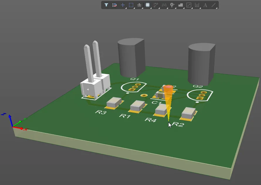
Hold Shift to display the 3D view directional sphere then click and drag the right mouse button to rotate.
Tips for Working in 3D
-
Press L to open the View Configuration panel when the board is in 3D Layout Mode, where you can configure the 3D view display options (on the View Options tab in the General Settings and 3D Settings sections).
-
The 3D display colors can use Realistic, or By Layer, which are the layer colors defined in the 2D Layout Mode. There are a number of 3D Configurations defined. Explore these in the General Settings of the View Options tab of the View Configuration panel. For example, the
Altium 3D Dk Green configuration is applied in the image above.
-
There are controls to configure the layer colors as well as the board thickness (vertical scaling), which is handy for examining the internal layers and interconnect structures in the PCB. 3D layers have a transparency setting; slide this to "see through" the objects on that layer.
-
You can choose to Show 3D bodies or hide them.
-
To display the components in 3D, each component needs to have a suitable 3D model included in its footprint. Refer to the Working with 3D Bodies page to learn more about including 3D models, and refer to Additional Tools for Working with 3D Bodies page to learn techniques for positioning a model on its footprint.
-
Apart from the component manufacturer's website, 3D models are also available on:
-
Community portal websites, such as 3D Content Central and GrabCAD, where designers share models.
-
A growing number of commercial 3D sites, including PCB 3D.