xDX Designer Schematic and Library Import Support
Support for the transfer of binary format designs captured using Siemens EDA® Xpedition® xDX Designer® (formerly DxDesigner®), to Altium Designer, is available courtesy of the latter's Import Wizard. Essentially formed from the separation of the binary importer from the existing ASCII importer (which remains unchanged), not only has the binary importer interface been upgraded to support data transfer from the latest version of xDX Designer, a wider range of object types are also now supported.
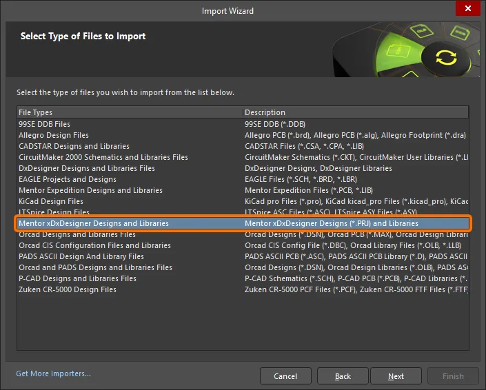
The xDX Designer design and library file importer is available through Altium Designer's Import Wizard (File » Import Wizard) by selecting the Mentor xDxDesigner Designs and Libraries option on the Wizard's Select Type of Files to Import page.

Select Mentor xDxDesigner Designs and Libraries in the Import Wizard to import xDX Designer files.
Import Wizard - Mentor xDxDesigner Projects and Designs
Mentor xDxDesigner Projects and Designs

Importing Mentor xDxDesigner Design Files

Click Add to choose which Mentor xDX Designer design files to include in the import process. You can delete a selected file by clicking Remove.
xDX Designer Importer supports importing project variants from xDX Designer projects. To import xDX Designer project variants, the following steps should be performed:
-
Using Variant Manager in xDX Designer, export variants via Report » Delimited Text Document.
-
Make sure that
Unplaced is defined as the Unplaced keyword in the Settings dialog.
-
Save the variant file as
ProjectVariants.txt in the same location as the .prj project file to be imported in Altium Designer.
-
On the Importing Mentor xDxDesigner Design Files page of Import Wizard, choose the xDX Designer project file (
.prj) – design variants will be imported automatically.
Importing Mentor xDxDesigner Library Files

Click Add to choose which Mentor xDX Designer library files to include in the import process. You can delete a selected file by clicking Remove.
Reporting Options

Use the Reporting Options page to configure the reports manager.
-
General Settings
-
Enable the desired logging options.
-
Do not run compile after import – enable to not compile after the import is done.
-
Treat same designators as multiparts – enable to treat alike designators as multiparts.
-
Import pin customizations (font size) – enable to import pin designators and names to Altium Designer with the same font size as in xDX Designer.
-
Schematic Settings
-
Recognize powerports – enable to recognize schematic powerports. Ensure that the default values in the Power port designators textbox are correct. If not, enter correct designators directly in the textbox.
-
Recognize ports – enable to recognize standard ports. Ensure that the default values in the Port designators textbox are correct. If not, enter correct designators directly in the textbox.
-
Ignore document templates – enable to ignore any document templates.
-
Hide default sheet template – enable to hide the default sheet template.
-
Do not translate hidden net name – enable to not translate hidden net name(s).
-
Force passive PinType for IM,OUT,BI pins – enable to force passive pintype.
-
Library settings
-
Generate Hetero components as multi-part – enable to import heterogeneous components as multi-parts.
-
Import symbols only – enable to import symbols only. When this option is enabled, identical symbols from the library database will be imported as a single schematic symbol, even if it is used by many components in the original library, and parameters are not imported to symbols in Altium Designer.
-
Property names to link with Altium fields – use the provided fields to define substitution parameters for component mapping for corresponding properties. You can list multiple parameters in the text box by using ; as a separator. If the first parameter does not exist, the next will be used in sequence.
-
Footprint link name – use to define substitution parameters for the footprint link property.
-
Designator property name - use to define substitution parameters for the designator property.
-
Comment name - use to define substitution parameters for the comment property.
-
Description name - use to define substitution parameters for the description property.
Executing Import Process

This page of Import Wizard will open if the Import symbols only option is enabled on the previous Reporting Options page. Use it to configure generation of a CSV file that contains data on pin mapping and component models/parameters.
Note that footprint names with specific prefixes (BGA, CAP, CAPC, CGA, COUP, DFN, DIO, DR, FILT, FUSE, INDC, INDM, ISOL, LEDC, LEDS, LGA, MECM, OSC, PQ, PS, QFN, QFP, RESC, RESM, SO, TO, VAR, and XTA) will include the component height values multiplied by 100 in the generated CSV file to uniquely name footprints with differing 3D Body heights. For example, a footprint with height of 1.4 and named CAPC2013N will be added to the CSV file as CAPC2013X140N.
-
Generate Pin Mapping and Component Models/Parameters Combined CSV – enable to generate the CSV file. When this option is enabled, the other options on the page become available:
-
Oracle DB Connection Settings – enter data required to connect to your Oracle DB: Server Address, Port, Database Name, User Name, and Password.
-
Parameter Mapping – define the path to the parameter mapping CSV file.
Finish

This page of the Wizard displays the Output Directory and Output Structure for the imported files. A green progress bar shows the progress of the import process while also listing each file at the process continues.

The Mentor xDX Designer Import Wizard has completed. The Messages panel appears with any relevant messages. Click Finish to close the Wizard. If any warnings were generated during the import process, a *.LOG file opens showing the warnings.
Version Support
The Importer has been updated for, and tested against, version 7.9.4 of xDX Designer (Expedition Enterprise 7.9.4, or simply EE7.9.4).
Supported Object Types
The following xDX Designer object types are supported when importing a design into Altium Designer:
-
Arc
-
Bus
-
Circle
-
Component Custom Parameter
-
Component Geometry
-
Component Pin
-
Line
-
Multi-Part Component (package)
-
Multi-Sheet Document
-
Offsheet Symbol
-
Polygon
-
Port and Power Port (existing as components)
-
Rectangle
-
Sheet Custom Parameter
-
Sheet Symbol
-
Sheet Template (stamp)
-
Text Label
-
Wire (with caption)
-
Altium Designer does not support multi-root references. Only a single top-level sheet is supported per design project. While the importer will often try to add an artificial 'root' sheet to accommodate, this can not be guaranteed for all combinations of complex, multi-level design structures.
-
For wire and bus objects, xDX Designer supports a degree of flexibility when positioning associated net labels. This freedom of positioning is not supported during the import.
Notes for xDX Designer Import
-
When imported to Altium Designer, a multi-part symbol receives a Design Item ID combined with the first and last part names defined in xDX Designer. These combined Design Item IDs are also used in the generated CSV files.
-
The ~ characters used for negation in xDX Designer are transformed into \ characters in pin names to correctly represent negation symbols in Altium Designer.
DxDesigner Schematic and Library Import Support
Translating complete Siemens EDA DxDesigner designs, including schematics and library files can all be directly imported by having Altium Designer's Import Wizard without having to convert to an intermediary format - thus avoiding the need for having DxDesigner installed. Such files will be converted into Altium Designer schematic documents (*.SchDoc) - one schematic document per sheet defined within the Logic file - and added to a PCB project (*.PrjPcb).
The DxDesigner file import capabilities are available through the DxDesigner importer – ![]() show image.
show image.
To learn more about changing installed core functionality, refer to the Installing Altium Designer page.
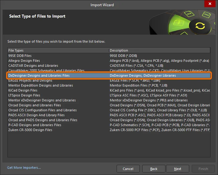
The Import Wizard (File » Import Wizard) removes much of the headache normally found with design translation by analyzing your files and offering many defaults and suggested settings such as project folders, project links to other libraries, drawing styles, and output project structure. Complete flexibility is found in all pages of the wizard, giving you as little or as much control as you would like over the translation settings before committing to the actual translation process. Select the DxDesigner Designs and Libraries Files option on the Wizard's Select Type of Files to Import page.

Select DxDesigner Designs and Libraries Files in the Import Wizard to import DxDesigner files.
Using the Import Wizard for DxDesigner Designs

You can drag and drop your designs directly from Windows Explorer project folders into the designs and libraries page of the Import Wizard.
You can use the Import Wizard whether using DxDesigner schematic files by themselves or in combination with a PADS Layout PCB. Because there is a difference in the way that project files and schematic files are named and organized between DxDesigner and Altium Designer, it's worth briefly reviewing this so that you understand exactly how your schematic design and libraries files will be translated after the import process.
DxDesigner manages the design project based on a user-defined directory path, and everything in the system uses this project path as the initial point of reference. For example, instead of using file extensions for a file's type, a folder called sch in the project path indicates that files under this folder are schematic files. The individual schematic files follow the naming convention of Name.N where N is a numeric number. An example of this would be schematic_design.1. DxDesigner identifies this as a schematic file only because it is in the specified project path and under the folder called sch. Likewise, a folder called sym in this project path indicates it is a symbol folder, and that all files under it are assumed to be the equivalent library files (also following the same naming convention as schematic files).
Altium Designer uses specific file extensions for certain file types such as schematic design files, library files and project files. As you begin to import your DxDesigner files using the Import Wizard, you will be asked for your project directory name. The Import Wizard knows to look for the sch and sym folders inside the specified project path. If that directory does not exist, you will be given a warning message.
Import Wizard - DxDesigner Designs and Libraries Files
DxDesigner Designs and Libraries Files

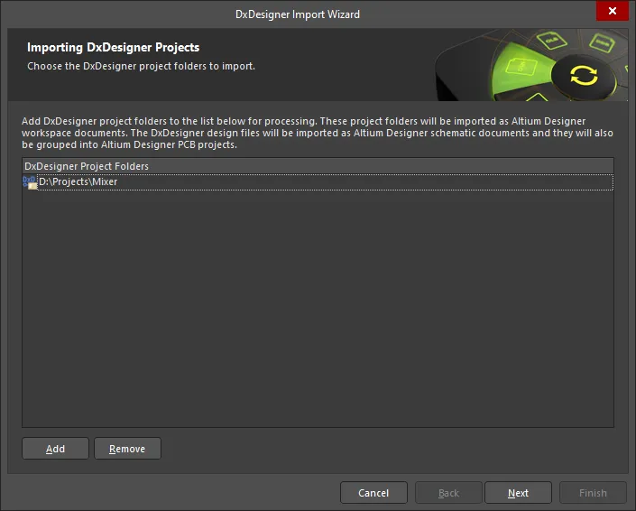
Importing DxDesigner Projects

Click Add to choose which DxDesigner project folders to include in the import process. You can delete a selected file by clicking Remove.
Importing DxDesigner Libraries

Click Add to choose which DxDesigner library folders to include in the import process. You can delete a selected file by clicking Remove.
Setting Reporting Options

Use the Reporting Options page to set up general log reporting options.
Under General Settings, enable the desired options: Log All Errors, Log All Warnings, Log All Events.
Configuring Import Options

-
General Options
DxDesigner projects can contain links to other libraries. Enable Add Linked Libraries to the List of Libraries for Import to import these libraries. This option can be customized on a project-by-project basis on another page in the Wizard.
Boxes in Altium Designer only support hollow or solid drawing modes. Use the Convert Gridded and Hatched Boxes to drop-down to select how gridded or hatched boxes are translated: Hollow or Solid.
-
Class Attribute Options
In the No BOM and No ECO textboxes, enter the Class attribute value(s) for the component that will not appear in either the BOM or ECO or both. You can enter multiple values separated by a comma.
Setting Linked Library Options

For each project folder listed, enable Import to import linked libraries.
Review Output Project Structure

Review the project structure listed on this page of the Wizard. Every design space document will reside in a separate directory within the specified output directory. The PCB projects and schematic documents imported from the DxDesigner designs also will be placed in the folder. Use the Browse Folder icon to search for and select the desired Output Directory.
Closing the Wizard

The DxDesigner Import Wizard has completed. Click Finish to close the Wizard.
Imported DxDesigner project paths and schematic files translate as follows:
-
Project paths have an equivalent Altium Designer PCB (
*.PrjPCB) project automatically created for them. Once translated, files are grouped into that PCB project. For example, if you specified C:\my_projects\LED_Matrix_Display as the DxDesigner project path, the Import Wizard will create LED_Matrix_Display.PcbPrj in Altium Designer.
-
Schematic files (
Name.N) translate to Altium Designer schematic files (*.SchDoc). Each schematic file will be imported as a single Altium Designer schematic file. Design hierarchy is maintained, including complex hierarchy.
Schematic Design File Translation
DxDesigner project paths and schematic files in the Import Wizard translate as follows:
-
Project paths have an equivalent Altium Designer PCB (
*.PrjPCB) project automatically created for them. Once translated, files are grouped into that PCB project. For example, if you specified C:\my_projects\LED_Matrix_Display as the DxDesigner project path, the Import Wizard will create LED_Matrix_Display.PcbPrj in Altium Designer.
-
Schematic files (Name.N) translate to Altium Designer schematic files (
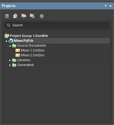
*.SchDoc). Each schematic file will be imported as a single Altium Designer schematic file. Design hierarchy is maintained, including complex hierarchy. Once the schematics have been opened, the schematic hierarchy will be shown.

Translated design files are displayed immediately after translation in the Projects panel.
Schematic Design Object Translation
Most component attributes are translated into parameters with a few exceptions:
-
Power Objects - DxDesigner symbols that contain a NETNAME attribute are identified as and translated into power objects in Altium Designer.
-
Ports - similar to power objects, a symbol with an attached attribute represents it as a port. DxDesigner symbols that contain an IN, OUT, or BI attribute are identified and translated into Input, Output, or Bidirectional ports respectively.
-
Signal - symbols that contain a SIGNAL attribute are identified as and translated into hidden power pins.
-
Reference Designator - the REFDES attribute attached in the DxDesigner symbol usually has the format of: REFDES = R? When it is placed into a sheet, the user will specify the REFDES of the component in the sheet i.e. REFDES = R21.
Other common design objects translate as follows:
-
DxDesigner wire segments and busses translate to wires and busses respectively.
-
A wire or bus segment in DxDesigner can have a label attached to it. This is translated into a net label. Net label strings in DxDesigner with the following format
D[0:8] are replaced with the following format D[0..8].
-
Composite symbol types are identified and translated as Altium Designer sheet symbols. The symbol pin is translated as sheet entries and the sheet symbol file name will point to the list of schematic sheets that matches the symbol file prefix.
Schematic Library File Translation
DxDesigner symbol library files translate as follows: symbol files (Name.N) translate to Altium Designer library files (*.SchLib). Each symbol file will be imported into a single Altium Designer library file. Once translated, files are grouped into the Altium Designer PCB project (*.PrjPCB) that is automatically created.
Schematic Symbol Translation
Component Name - the following table describes how the DxDesigner symbol translates to the Altium Designer component:
DxDesigner Symbol
|
Altium Designer Component
|
Symbol file name.
For example, if the symbol file name is cap.1, the component name will be cap.1.
The exception is for the hetero symbols that will be described later.
|
Component name
|
REFDES attribute
|
Designator
|
Use from the DEVICE attribute
|
Comment
|
Any other symbol attribute
|
Parameters
|
Pin Type - the following table maps the PINTYPE attribute from DxDesigner to Altium Designer:
DxDesigner Pin Type Attribute Value
|
Altium Designer Pin Type
|
BI
|
IO
|
TRI
|
HiZ
|
ANALOG
|
Passive
|
OCL
|
Open Collector
|
OEM
|
Open Emitter
|
-
Graphical Objects - most objects have a direct translation from DXDesigner to Altium Designer. Boxes (as defined as lower left and upper right corners) translate to four-point polygons.
-
Multiple-part symbols - the PARTS attribute attached to the symbol indicates the number of parts this symbol represents and translates to the number sub-parts in Altium Designer.
-
Annotate Symbol Type - DxDesigner categorizes the symbol into four types: composite, pin, annotate, and module. The most common use of symbols in DxDesigner is for sheet borders and graphical annotation. Because of this reason, such symbols are translated in Altium Designer components with a TYPE = Graphical.
-
Heterogeneous Symbols - heterogeneous symbols in DxDesigner are any group of symbols that have the same HETERO attribute. When symbols are grouped under one HETERO type, they represent one device. Altium Designer translates these symbols to multiple parts or display modes under one component depending on the heterogeneous type. There are three distinct types:
-
HETERO TYPE 1- different components within the same device. The Altium Designer attribute assigned to this type follows the format: HETERO = sym1, sym2, [sym3].
-
HETERO TYPE 2 - different gates within the same device. The Altium Designer attribute assigned to this type follows the format: HETERO = sym, (symP) where P = PARTS number.
-
HETERO TYPE 3 - this is a split IC. The Altium Designer attribute assigned to this type follows the format: HETERO = (icsymname), (icsymname). The main difference between this type and HETERO TYPE 1 is only the context used by DxDesigner related to ICs.
Working with Documents in Altium Designer
In Altium Designer, the logical design area begins with a document, and for each document there is a file stored on the hard drive. This means that for each Altium Designer schematic sheet (page) there is a file. There can also be multiple design documents of varying types, depending on the nature of the design you are working on. Getting started, most DxDesigner users will be interested in the schematic and PCB document types as these are the files that their designs will be translated to.

Basic file operations: new PCB and schematic document types can be easily created via File » New, or by right-clicking on the project in the Projects panel.
The Schematic Symbol is the Part
In DxDesigner, a symbol block type is the logical entity that is described graphically by attributes, pins and various properties. As block types are placed in a schematic design, DxDesigner maintains the identity of the part for back annotation, net listing, bills of materials, and so forth. At the very minimum, a part requires a part name, a part reference prefix, and a name of a PCB footprint.
In Altium Designer, the logical symbol is assumed to be the essential starting point of a component. It can be initially defined at minimum as a name in a schematic library to which pins and any graphical symbols or alternative display options needed for implementation may be added. This flexibility allows a component to be represented in different ways during the design and capture process. This may not only be as a logical symbol on the schematic, but also be a footprint on the PCB or even as a SPICE definition for simulation.