Parent page: Tutorial - A Complete Design Walkthrough with Altium Designer
Main pages: PCB Design Rules Reference, Design Rule Checking (DRC)
The PCB editor is a rules-driven design environment in which you can define many types of design rules that can be checked to ensure the integrity of your board. Typically you set up the design rules at the start of the design process. The online DRC feature monitors the enabled rules as you work and immediately highlights any detected design violations. Alternatively, you can also run a batch DRC to test that the design complies with the rules and generate a report that details the enabled rules and any detected violations.
Earlier in the tutorial, you examined the routing design rules, adding a new width constraint rule targeting the power nets, as well as an electrical clearance constraint and a routing via style rule. As well as these, there are a number of other design rules that are automatically defined when a new board is created.
Configuring the Display of Rule Violations
Preferences page: PCB Editor – DRC Violations Display
Before checking for rule violations, it is important to understand how violations are displayed.
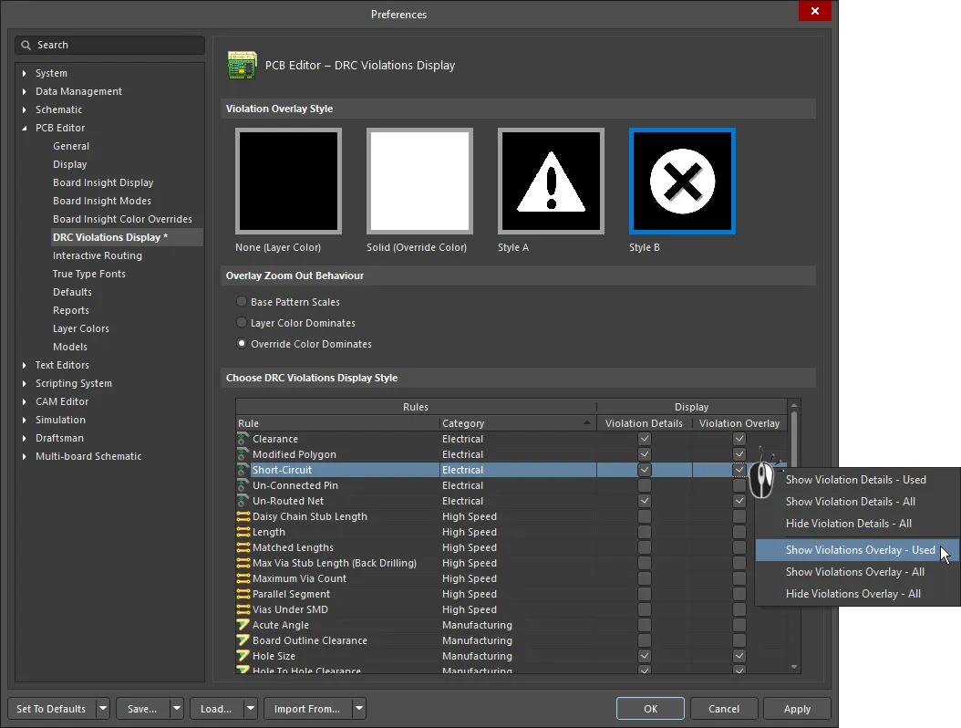
Altium Designer has two techniques for displaying design rule violations, each with its own advantages. These are configured on the PCB Editor – DRC Violations Display page of the Preferences dialog:
- Violation Overlay – violations are identified by the primitive-in-error highlighted in the color chosen for the DRC Error Markers (configured in the View Configuration panel; press L to open). The default behavior is to show the primitives in a solid color when zoomed out, changing to the selected Violation Overlay Style as you zoom in. The default is Style B – a circle with a cross in it.
-
Violation Details – as you zoom further in, Violation Detail is added (if enabled), detailing the nature of the error. Violation Detail can include:
- Information at the site of the violation
- Where appropriate, an icon to indicate the type of violation, for example, thin lines that cross over, indicating a short circuit.
- A numerical value showing the rule setting that is failing, for example, <0.25mm.
Violations can be displayed as a colored overlay and also as a detailed message, with different symbols being used to show different detail of the error type.


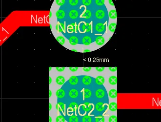
Violations are shown in solid green (the first image), as you zoom in this changes to the selected Violation Overlay Style (the second image); as you zoom in further Violation Details are added (the third image).
Preparing to run a Design Rule Check (DRC)
- Select
 » View Configuration (shortcut: L) and confirm that the DRC Error visibility option (System Colors section) is enabled so that DRC error markers are displayed.
- Confirm that the Online DRC (Design Rule Checking) system is enabled on the PCB Editor – General page of the Preferences dialog. Keep the Preferences dialog open, and switch to the PCB Editor – DRC Violations Display page of the dialog.
- The PCB Editor – DRC Violations Display page of the Preferences dialog is used to configure how violations are displayed in the design space. There are two different methods available for displaying violations, each with its own strengths.
- For the tutorial, right-click in the Choose DRC Violations Display Style area of the PCB Editor – DRC Violations Display page of the Preferences dialog and select Show Violation Details - Used, then right-click again and select Show Violation Overlay - Used, as shown in the dialog image above.
- Click OK to save changes and close the Preferences dialog. You are now ready to check the design for errors.
The rules that are needed will depend on the nature of your design; there is no specific set of rules that suits every design. Keep this in mind as you are checking rule violations. Ask yourself, do I need this rule to be enabled? If you are attempting to work out the function of a rule in the PCB Rules and Constraints Editor and are unsure, click anywhere in the constraints area of the rule and press F1 for more information about that specific rule.
Configuring the Rule Checker
The design is checked for violations by running the Design Rule Checker. Run the Tools » Design Rule Check command to open the dialog. Both online and batch DRC are configured in this dialog.
DRC Report Options
- By default, the dialog opens showing the Report Options page selected in the tree on the left of the dialog (shown below).
-
The right side of the dialog displays a list of general reporting options. For more information about the options, press F1 when the cursor is over the dialog. These options can be left at their defaults.

Rule checking, both online and batch, is configured in the Design Rule Checker dialog.
DRC Rules to Check
- The testing of specific rules is configured in the Rules to Check section of the dialog. Select this page in the tree on the left of the dialog to list all of the rule types (shown below). You can also examine them by type, for example, Electrical, by selecting that page on the left of the dialog.
- For most rule types, there are checkboxes for Online (check as you work) and Batch (check this rule when the Run Design Rule Check button is clicked).
-
Click to enable/disable the rules as required. Alternatively, right-click to display the context menu. This menu allows you to quickly toggle the Online and Batch settings. Select the Batch DRC - Used On entry, as shown in the image below.
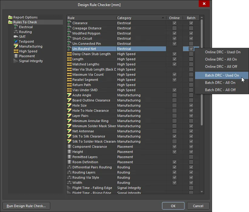
Checking is configured for each rule type. Use the right-click menu to enable the Used design rules.
Running a Design Rule Check (DRC)
Click the Run Design Rule Check button at the bottom of the dialog to perform a design rule check. When the button is clicked, the DRC will run, then:
- The Messages panel will open and list all detected errors.
- If the Create Report File option was enabled in the Report Options page of the dialog, a Design Rule Verification Report will open in a separate document tab. The report for the tutorial is shown below.
- The upper section of the report details the rules that are enabled for checking and the number of detected violations. Click on a rule to jump to and examine those errors.
- Below the summary of violating rules are specific details about each violation.
- The links in the report are live. Click on a specific error to jump back to the board and examine that error on the board. Note that the zoom level for this click action is configured on the System – Navigation page of the Preferences dialog. Experiment to find a zoom level that suits you.
 The upper section in the report details the rules that are enabled for checking and the number of detected violations. Click on a rule to jump to and examine those errors.

The lower section of the report shows each rule that is being violated, followed by a list of the objects in error. Click on an error to jump to that object on the PCB.
Locating the Error Condition
When you are new to the software, a long list of violations can initially seem overwhelming. A good approach to managing this is to disable and enable rules in the Design Rule Check dialog at different stages of the design process. It is not advisable to disable the design rules themselves if there are violations, just the checking of them. For example, you would always disable the Un-Routed Net check until the board is fully routed.
- When a batch DRC is run on the tutorial board, there are:
- 4 Minimum Solder Mask Sliver violations – the minimum width of a strip of solder mask is less than allowed by this rule. This typically occurs between component pads.
- 4 Clearance Constraint violations – the measured electrical clearance value between objects on signal layers is less than the minimum amount specified by this rule.
- To locate a violation:
- Using the Violation Details, you can establish the error condition.
-
The image below shows the Violation Details for one of the clearance constraint errors, indicated by the white arrows and the 0.25mm text, indicating that this gap is less than the minimum 0.25mm allowed by the rule. The next step is to work out what the actual value is so you know how much it has failed. You can then decide how to resolve this error.
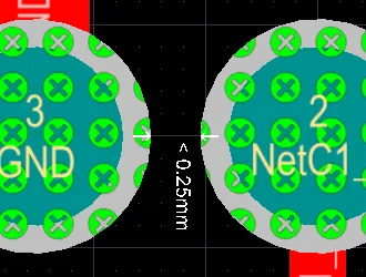
The Violation Details show that the clearance between these two pads is less than 0.25mm; it does not detail the actual clearance.
Understanding the Error Condition
So you've found an error. How do you know how much it has failed? As the designer, you need this essential information to be able to decide how best to resolve the error.
For example, if the rule says the allowable minimum solder mask sliver is 0.25 mm and the actual sliver is 0.24 mm, then the situation is not that bad and you may be able to adjust the rule setting to accept this value. But if the actual sliver value is 0.02, then that is probably not a situation that can be resolved by adjusting the rule setting.
The PCB editor includes three handy measurement tools: Measure Distance, Measure Selected Objects, and Measure Primitives, which are available in the Reports menu.
- Measure Distance – measure the distance between the two locations you click after running the command; keep an eye on the Status Bar for instructions. The location that you can click is constrained by the current snap grid.
- Measure Selected Objects – measure the length of selected tracks and arcs. Use this to work out route lengths, select the required objects manually, or use the Select » Physical Connection or Select » Connected Copper commands.
- Measure Primitives – measure the edge-to-edge distance between the two primitives you click on after running the command; keep an eye on the Status Bar for instructions.
-
Measurement results are overlaid directly in the design space. The colors that are used are configured in the System Colors section of the View Configuration panel. Overlaid dimensions are retained on screen to allow multiple measurements to be performed. Press Shift+C to clear the measurement results.
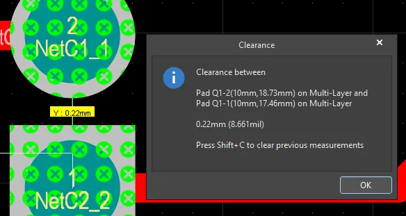
Measuring the distance between the edges of adjacent pads using the Measure Primitives command.
Apart from actually measuring the distance, there are a number of approaches to finding out how much a rule has failed by. You can use:
- The right-click Violations submenu, or
- The PCB Rules And Violations panel, or
- The detail included in the Messages panel; the actual value is detailed along with the specified value (for example, 0.175 mm < 0.254 mm).
The Violations Submenu
The right-click Violations submenu was described earlier in the Existing Design Rule Violation section.
The image below shows how the Violations submenu details the measured condition against the value specified by the rule.

Right-click on a violation to examine what rule is being violated and the violation conditions.
The PCB Rules And Violations Panel
Panel page: PCB Rules And Violations
The PCB Rules And Violations panel is an excellent feature for locating and understanding error conditions.
- Click the
 button then select PCB Rules And Violations from the menu to display the panel. It will default to show
 [All Rules] in the Rule Classes list. Once you have identified a rule type of interest, select that specific rule class so that only those violations are shown at the bottom of the panel.
-
Click once on a violation in the list to jump to that violation on the board; double-click on a violation to open the Violation Details dialog.
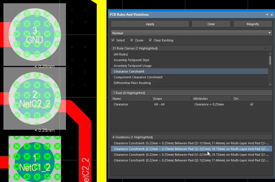
The panel details the violation type, the measured value, the rule setting, and the objects that are in violation.
Note that at the top of the PCB Rules And Violations panel there is a drop-down, which can be used to select Normal, Dim, or Mask. Dim and Mask are display filter modes, where everything other than the object(s) of interest are faded, leaving only the chosen object(s) at normal display strength. The Dim mode applies the filter but still allows all design space objects to be edited. The Mask mode filters out all other design space objects, only allowing the unfiltered object(s) to be edited.
The amount that the display is faded is controlled by the Dimmed Objects and Masked Objects slider controls in the Mask and Dim Settings section of the View Options tab of the View Configuration panel. Experiment with these sliders when you have the Mask mode or Dim mode applied.

To clear the filter, you can either click the Clear button at the top of the PCB Rules And Violations panel or press the Shift+C shortcut. This filtering feature is very effective in a busy design space and can also be used in the PCB panel and the PCB Filter panel.
Resolving the Violations
As the designer, you have to work out the most appropriate way of resolving each design rule violation. Let's start with the solder mask errors as they are related, and both error conditions may be affected by the changes you make to solder mask settings.
Minimum Solder Mask Sliver Violations
Design rule reference: Minimum Solder Mask Sliver
The solder mask is a thin, lacquer-like layer applied to the outer surface of the board, providing a protective and insulating covering for the copper. Openings are created in the mask for components and wires to be soldered to the copper. It is these openings that are displayed as objects on the solder mask layer in the PCB editor (note that the solder mask layer is defined in the negative – the objects you see become holes in the actual solder mask).
During fabrication, solder mask is applied using different techniques. The lowest cost approach is to silkscreen it onto the board surface through a mask. To allow for layer alignment issues, the mask openings are typically larger than the pads, reflected by the 4mil (~0.1mm) expansion value used in the default design rule.
There are other techniques for applying solder mask, which offer higher-quality layer registration and more accurate shape definition. If these techniques are used, the solder mask expansion can be smaller or even zero. Reducing the mask opening reduces the chance of having solder mask slivers or silk to solder mask clearance errors.
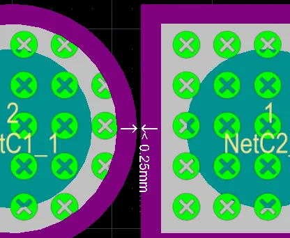
A solder mask sliver error. The purple represents the solder mask expansion around each pad.
Errors such as these solder mask issues cannot be resolved without consideration of the fabrication technique that will be used to make the finished board.
For example, if this was a complex, multi-layer board for a high-value product, then it is likely that a high-quality solder mask technology would be employed, which would allow a small or zero solder mask expansion. However, a simple, double-sided board like the board in this tutorial is more likely to be fabricated as a low-cost product, requiring a low-cost solder mask technology to be used. That means resolving the solder mask sliver errors by reducing the solder mask expansion for the entire board is not an appropriate solution.
Like many aspects of PCB design, the solution lies in making thoughtful trade-offs in a focused way to minimize their impact.
Enable the display of the solder mask before attempting to check solder mask errors and resolve them. If it is not visible, press L to open the View Configuration panel where that layer can be enabled.
Resolving the Solder Mask Sliver violations
To resolve this violation you can:
- Increase the solder mask opening to completely remove the mask between the transistor pads, or
- Decrease the minimum acceptable sliver width, or
- Decrease the mask opening to widen the sliver to an acceptable width.
This is a design decision that would be made in light of your knowledge of the component and the fabrication and assembly technology that is going to be used. Opening the mask to completely remove the sliver of mask between the transistor pads means that there is more chance of creating solder bridges between those pads, whereas decreasing the mask opening will still leave a sliver, which may or may not be acceptable, and will also introduce the possibility of mask-to-pad registration problems.
For this tutorial, you will do a combination of the second and third options, decreasing the minimum sliver width to a value suitable for the settings being used on this board, and also decreasing the mask expansion, but only for the transistor pads.
- The first step is to reduce the allowable sliver width. To do this, open the PCB Rules and Constraints Editor, then in the Manufacturing section locate and select the existing Minimum Solder Mask Sliver rule, called
MinimumSolderMaskSliver.
-
A value equal to the pad separation of 0.22mm (~8.7mil) will be acceptable for a design such as this; edit the Minimum Solder Mask Sliver value to be 0.22mm in the Constraints region of the rule.
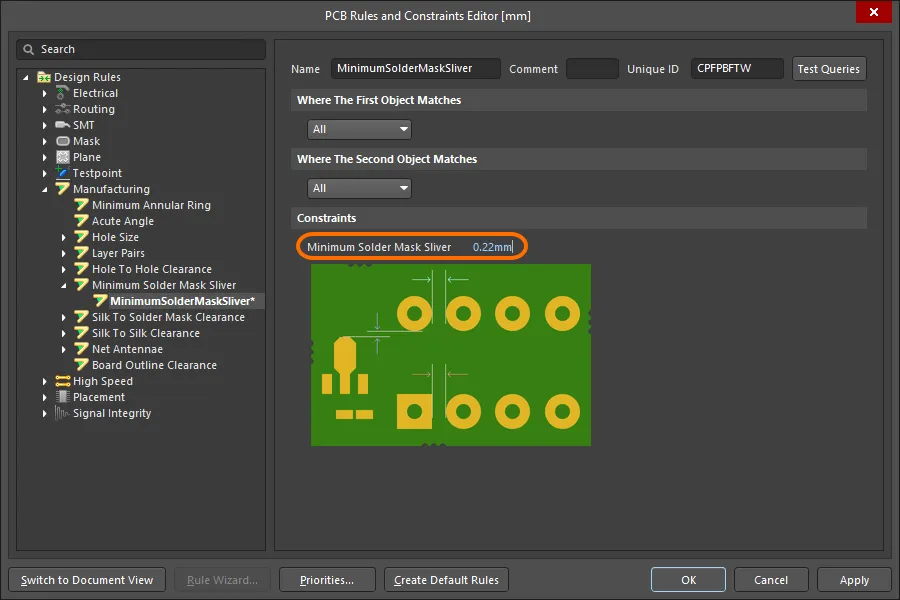
- The next step is to add a mask expansion rule for just the transistors that reduces the mask expansion to zero. Doing this will mean that the opening in the solder mask is the same size as the pad, making the width of solder mask sliver between the pads equal to the separation distance between the pads (
0.22mm). Click on Mask in the tree on the left of the PCB Rules and Constraints Editor dialog to show the current Solder Mask Expansion rules; there should be one rule called SolderMaskExpansion.
- Double-click on it to select the rule and display its settings; it will specify an expansion value of
0.102mm (4mil). Since it is only the transistor pads that are in violation, you will not edit this value; instead, you will create a new rule.
- To add a new Solder Mask Expansion rule, right-click on the existing rule in the tree on the left and select New Rule from the context menu. A new rule called
SolderMaskExpansion_1 will be created; click on it to display its settings.
- Edit the rule settings to be as shown below:
- Name –
SolderMaskExpansion_Transistor
- Where the Object Matches – select
Footprint in the drop-down, then select ONSC-TO-92-3-29-11 (the name of the transistor footprint) in the second drop-down that appears
- Expansion top / bottom –
0mm
- Click Apply to accept the changes and keep the PCB Rules and Constraints Editor open.
Clearance Violations
Design rule reference: Clearance Constraint
There are two ways of resolving this clearance constraint:
- Decrease the size of the transistor footprint pads to increase the clearance between the pads, or
- Configure the rules to allow a smaller clearance between the transistor footprint pads.
Since the 0.25mm clearance is quite generous and the actual clearance is quite close to this value (0.22mm), a good choice in this situation would be to configure the rules to allow a smaller clearance. This can be done in the existing Clearance Constraint design rule, as shown below.
- The TH Pad – to – TH Pad value is changed to
0.22mm in the grid region of the rule constraint. To edit a cell, select first it then press F2.
-
This solution is acceptable in this situation because the only other component with thruhole pads is the connector, which has pads spaced over 1mm apart. If this was not the case, the best solution would be to add a second clearance constraint targeting just the transistor pads, as was done for the solder mask expansion rules.
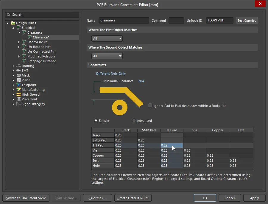
Edit the Clearance Constraint to allow a TH Pad to TH Pad clearance of 0.22mm.
- Click OK to accept the changes and close the PCB Rules and Constraints Editor dialog.
Silk to Silk Clearance Violation
Design rule reference: Silk to Silk Clearance
The last error to resolve is the silk to silk clearance violations. These are usually caused by a designator being too close to the outline of an adjacent component. Your design may not have any of these violations – it depends on how close you placed the components, or if you have already repositioned the designators. Click, hold and drag a designator to move it – all objects will dim apart from the objects in the component whose designator is being moved; move that designator to a new location.
Designator movement will be constrained by the current snap grid. If it is currently too coarse, press Ctrl+G and enter a new grid value.

Reposition any designator that is causing a silk to silk violation.
Running a Design Rule Check after resolving the violations
- Save the PCB file locally.
- Open the Design Rule Checker dialog (Tools » Design Rule Check) and make sure that the Create Report File option is enabled on the Report Options page.
- Click the Run Design Rule Check button.
- A new report will be generated and open in a separate document tab. Make sure that it does not contain any rule violations.
- If there are violations, back to the PCB document and resolve these violations, then generate the report again.
-
Remove the generated DRC report from the project (it will be generated during the design release process) – in the Projects panel, find the report file in the Generated\Documents sub-folder, right-click on it and select the Remove from Project command. In the Remove from project dialog that opens, choose the Delete file option.

Remove the Design Rule Check report file from the project, with the permanent delete option.
- Save the PCB and the project to the Workspace.
- Close the PCB file.
Always confirm that you have a clean Design Rule Verification Report before generating outputs.
Well done! You have completed the PCB layout and are ready to configure output documentation and release the project.
