Applied Parameters: None
Summary
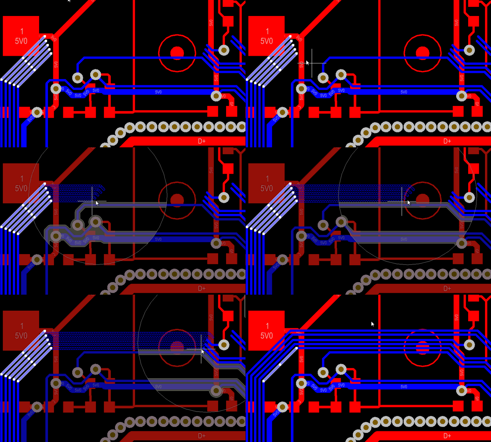
When routing a PCB it is fairly common for groups of signals to all need to be routed along the same path, such as for Address and Data busses. One option would be to route each of these signals individually but a much faster option is to route them collectively. This command allows you to do just that - route multiple nets simultaneously.
Access
This command can be accessed from the PCB Editor by:
- Choosing the Route » Interactive Multi-Routing command, from the main menus.
- Clicking the
 button on the Wiring toolbar.
- Right-clicking in the workspace and choosing the Interactive Multi-Routing command from the context menu.
Use
First select the source pad of each net to be included in the route. Shift+click to select individual pads, Ctrl+click and drag to draw a selection rectangle and sub-select multiple child pads in a component. After launching the command, you will be prompted to click to begin multi-routing. Simply click within the workspace at the point where you require to lay down the first set of track segments, then continue routing as required toward your target destination.
As you route, the standard conflict resolutions modes are available, including Walkaround Obstacles, Push Obstacles, Hug and Push Obstacles, Ignore obstacles, and Stop at First Obstacle. Use Shift+R to cycle through the modes.
Use the + and - keys on the numeric keypad to switch routing layers, and the B / Shift+B to decrease / increase bus spacing in increments of the current grid. Press C to converge bus spacing to the minimum allowed by the applicable routing rules.
Press Shift+F1 to display all of the available shortcuts for commands available to you while in multi-trace routing mode.
Placement Modes
While placing track segments there are 5 available corner modes, 4 of which also have corner direction sub-modes. During placement:
- Press Shift+Spacebar to cycle through the 5 available corner modes: 45 degree, 45 degree with arc, 90 degree, 90 degree with arc, and Any Angle.
- Press Spacebar to toggle between the two corner direction sub-modes.
- When in either of the arc corner modes, hold the
 or
or  keys to shrink or grow the arc. Hold the Shift key as you press to accelerate arc resizing.
- Press the 1 shortcut key to toggle between placing 1 segment per click, or 2 segments per click. In the first mode the hollow track segment is referred to as the look-ahead segment.
- Press the Backspace key to remove the last vertex.
Loop Removal
Altium Designer provides support for Loop Removal when interactively routing multiple nets. As you route there will be many instances where you need to change some of the existing routing. Rather than attempting to change the existing routing using a drafting type approach of clicking and dragging track segments, you re-route. To do this, launch the Interactive Differential Pair Routing command, click on the existing routing to start, and then route the new path, coming back to meet the existing routing. This will create a loop with the old path and the new path - no need to worry though, as soon as you right-click or press Esc to terminate the route, the redundant segments are automatically removed, including any redundant vias.
This feature is employed by enabling the
Automatically Remove Loops option, on the
PCB Editor - Interactive Routing page of the
Preferences dialog. To toggle this feature on or off while routing, use the
Shift+D keyboard shortcut.
Displaying Clearance Boundaries
As you route, it can be extremely beneficial to have an indication of just how much space you really do have available to you. Altium Designer provides this very aid, through dynamic display of clearance boundaries. As you interactively route, the no-go clearance area defined by the existing objects + the applicable clearance rule is displayed as shaded polygons. By default, all clearance boundaries are displayed, but you can opt to reduce the clearance display area - only viewing boundaries that fall within a localized viewing circle.

The clearance around existing workspace objects is displayed dynamically, as you route. Use the Ctrl+W shortcut to enable/disable
during routing.
This feature is employed by enabling the
Display Clearance Boundaries option, on the
PCB Editor - Interactive Routing page of the
Preferences dialog. To toggle this feature on or off while routing, use the
Ctrl+W keyboard shortcut. To show clearance boundaries only with a localized area, ensure to enable the
Reduce Clearance Display Area sub-option.
The display of clearance boundaries is available in all routing modes except Ignore Obstacles.
Tips
- Interactive routing preferences are defined on the PCB Editor - Interactive Routing page of the Preferences dialog. These preferences can be accessed while routing by using the Tab shortcut.
- It is also possible to enter this mode of routing implicitly, by selecting a group of tracks and dragging their ends (sometimes referred to as Smart Drag). In this mode successive drags can be used to add new segments.
