
Tutorial - Setting Up the Design Rules in Altium Designer
Main pages: Defining, Scoping & Managing PCB Design Rules, PCB Design Rule Types
Altium Designer's PCB editor is a rules-driven environment. With a well-defined set of design rules, you can successfully complete board designs with varying and often stringent design requirements.
Design rules are configured in the PCB Rules and Constraints Editor dialog. The rules are divided into categories, which are then further divided into design rule types.
Defining the Width Design Rules
The width of the routing is controlled by the applicable Width design rule, which is automatically selected when you start routing a net.

Defining the Width Design Rule for the Signal Nets
-
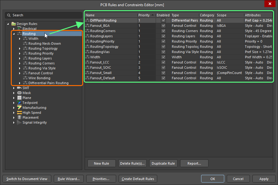
With the PCB as the active document, open the PCB Rules and Constraints Editor dialog by selecting the Design » Rules command from the main menus .

-
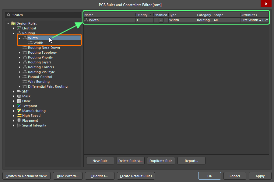
Each rules category is displayed under the Design Rules structure (left-hand side) of the dialog. Double-click on the Routing category entry to expand it and see the related routing rules, then double-click on the Width rule type entry to display the currently defined width rules.
-
Click once on the existing Width rule to select it. When you click on the rule, the right-hand side of the dialog displays the settings for that rule including the rule's Where The Object Matches in the top section (also referred to as the rule's scope – what you want this rule to target) with the rule's Constraints below that.

The default Width design rule -
Since this rule is to target the majority of nets in the design (the signal nets), confirm that the Where The Object Matches setting is set to All as shown in the image above.
-
Set the constraints for the rule by entering the following values:
-
Min Width =
0.2 -
Preferred Width =
0.25 -
Max Width =
0.25

-
-
The rule is now defined. Click Apply to save it and keep the dialog open.
Defining the Width Design Rule for the Power Nets
The next step is to add another design rule to specify the routing width for the power nets.
-
With the existing Width rule selected in the Design Rules tree on the left of the PCB Rules and Constraints Editor dialog, right-click and select New Rule to add a new Width rule.

-
A new rule named
Width_1appears. Click on the new rule in the Design Rules tree to configure its properties.
-
Click in the Name field and enter the name
Width_Powerin the field.
-
Set the rule scope so the rule targets objects that belong to the 12V or GND net. We will use the Query Builder dialog to build the query for the scope. To do this (the process is also shown in the video below):
-
Click in the drop-down in the Where The Object Matches region and select Custom Query from the list. The dialog will change to include an edit box where the custom query is entered.
-
Click the
 button to open the Query Builder dialog.
-
Click the Add first condition text, select Belongs to Net, then set the Condition Value to 12V.
-
Click the Add another condition text, select Belongs to Net, then set the Condition Value to GND.
-
The AND operator will have appeared between the two condition statements. Click on it and select OR from the drop-down.
-
Click the OK button to accept the query and return to the PCB Rules and Constraints Editor dialog. The rule scope will change to
(InNet('12V') OR InNet('GND')).
-
-
Set the constraints for the rule to allow power net routing widths in the range of 0.25 to 0.5 mm. To do this, enter the following values:
-
Min Width =
0.25 -
Preferred Width =
0.5 -
Max Width =
0.5

-
-
Click Apply to save the rules and keep the dialog open.
Defining the Clearance Design Rule
The next step is to define how close electrical objects belonging to different nets can be to each other. This requirement is handled by the Clearance design rule. For the tutorial, a clearance of 0.25 mm between all objects is suitable.
-
Expand the Electrical category in the tree of design rules, then expand the Clearance rule type.

-
Click to select the existing rule of this type.
For this design, this rule will be configured to define a single clearance between
Allobjects.
-
In the Constraints region of the dialog, set the Minimum Clearance to
0.25.
-
Click Apply to save the rule and keep the dialog open.
Defining the Routing Via Style
As you route and change layers, a via is automatically added. In this situation, the via properties are defined by the applicable Routing Via Style design rule.
-
Expand the Routing category in the tree of design rules then expand the Routing Via Style rule type and select the existing design rule of this type.

-
Set the constraints for the rule to set the allowed via diameter to 1 mm and the allowed via hole size to 0.6 mm. In this case, we will set all fields (minimum, maximum, and preferred) to the same size:
-
Via Diameter: Minimum, Maximum, Preferred =
1 -
Via Hole Size: Minimum, Maximum, Preferred =
0.6

-
-
Click OK to save the changes and close the PCB Rules and Constraints Editor dialog.
-
Save the PCB document locally by right-clicking its entry in the Projects panel and selecting Save from the context menu.