Working with the Width Design Rule on a PCB in Altium Designer
Rule category: Routing
Rule classification: Unary
Summary
This rule defines the width of tracks placed on the copper (signal) layers.
Constraints

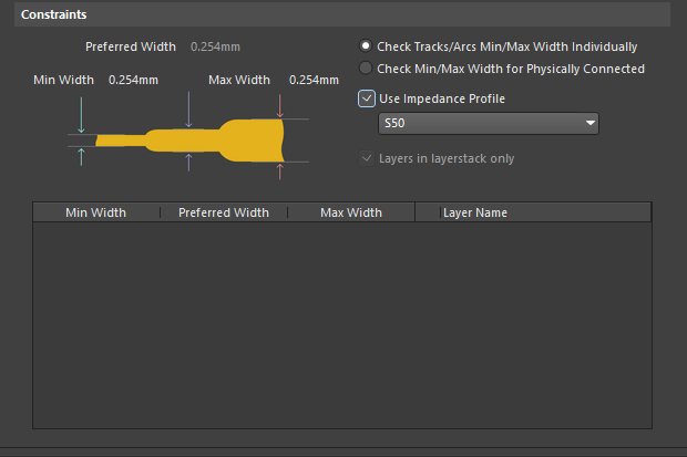
Constraints for the Width rule.
- Preferred Width - specifies the preferred width to be used for tracks when routing the board.
- Min Width - specifies the minimum permissible width to be used for tracks when routing the board.
- Max Width - specifies the maximum permissible width to be used for tracks when routing the board.
- Check Tracks/Arcs Min/Max Width Individually - checks individual widths of tracks and arcs fall within the minimum and maximum range.
- Check Min/Max Width for Physically Connected - checks the width of routed copper formed by a combination of tracks, arcs, fills, pads, and vias falls within the minimum and maximum range.
- Use Impedance Profile - if the design needs to be routed to strict impedance requirements, ensure this option is enabled. When enabled, use the drop-down to select the impedance profile desired, When the rule is configured in this mode, the routing width required on each routing layer is calculated based on the specified impedance profile, which is set in the Layer Stack Editor. Once the rule is defined, as you route a net that falls under the scope of the rule, the track width will automatically be set to the width required to meet the specified impedance for that layer.
- Layers in layerstack only - allows you to display and edit the width constraints for just the defined signal layers in the layer stack. When enabled, only the layers in the stack will be displayed in the Layer Attributes Table. When disabled, all signal layers will be displayed.
- Layer Attributes Table - displays all signal layers or only those defined in the layer stack, as controlled by the Layers in layerstack only option. The minimum, maximum and preferred routing widths are displayed, as well as other layer-specific information. The routing width fields can be set globally by defining a value in the individual width constraint fields, or individually by typing a width value directly into the table. When the Use Impedance Profile option is enabled, the required width entries will be automatically calculated and entered for each layer in the table. They cannot be defined on an individual basis while in this mode.
How Duplicate Rule Contentions are Resolved
All rules are resolved by the priority setting. The system goes through the rules from highest to lowest priority and picks the first one whose scope expression matches the object(s) being checked.
Rule Application
The Preferred Width setting is obeyed by the Autorouter.
The Min Width and Max Width settings are obeyed by the Online DRC and Batch DRC. They also determine the range of permissible values that can be used during interactive routing (press Tab key while routing to change the trace width within the defined range, through the Properties panel). If a value is entered outside of this range, it will automatically be clipped.
Tips
- The width of each net in a differential pair is monitored by the applicable Differential Pairs Routing rule.
