SOT143/343
SOT143/343 Package Overall Dimensions
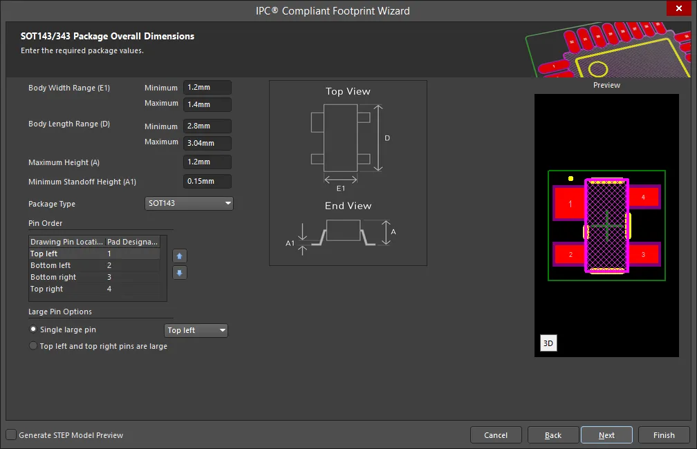
Use the SOT143/343 Package Overall Dimensions page to set the required values for Body Width Range, Body Length Range, Maximum Height, and Minimum Standoff Height. Use the drop down to select the correct Package Type: SOT143 or SOT343.
To specify the Pin Order, use  and
and  to move the selected Pad Designator up or down in the list.
Large Pin Options can be specified by selecting Single large pin or Top left and top right pins are large. If Single large pin is selected, use the drop down to specify the location: Top left, Bottom left, Bottom right, or Top right. The Preview region is dynamically updated.
SOT143/343 Package Pin Dimensions
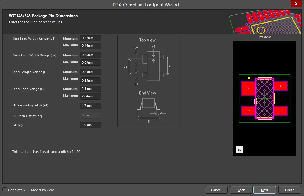
Enter the required values for the package pin dimensions on the SOT143/343 Package Pin Dimensions page.
SOT143/343 Package Heel Spacing
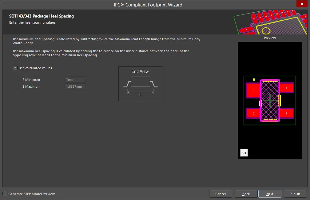
Set the desired heel spacing values on the SOT143/343 Package Heel Spacing page.
Enable the Use calculated values checkbox to use the values currently displayed or enter new values directly in the textboxes for S Minimum and S Maximum.
SOT143/343 Solder Fillets
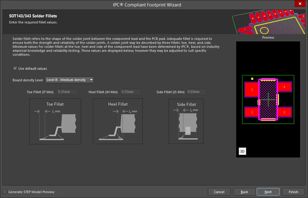
Set the required solder fillet values on the SOT143/343 Solder Fillets page. Solder fillet refers to the shape of the solder joint between the component lead and the PCB pad. Adequate fillet is required to ensure both the strength and reliability of the solder joints. A solder joint may be described by three fillets: toe, heel, and side.
Minimum values for solder fillets at the toe, heel and side of the component lead have been determined by IPC based on industry empirical knowledge and reliability testing. Enable Use default values to use the values displayed or you can adjust them to suit your specific needs.
Use the Board density Level drop-down to select the desired board density. Choose from Level A - Low density, Level B - Medium density, and Level C - High density. The Preview region is dynamically updated to show your changes.
To update the values for Toe Fillet (JT Min), Heel Fillet (JH Min), and Side Fillet (JS Min), the Use default values option must be disabled. Enter the new values directly in the textboxes.
SOT143/343 Component Tolerances
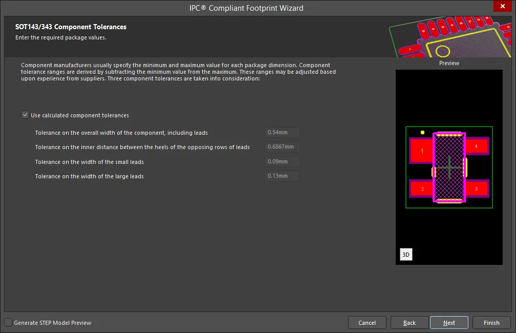
Enter the required values for component tolerances on the SOT143/343 Component Tolerances page.
Component manufacturers usually specify the minimum and maximum value for each package dimension. Component tolerance ranges are derived by subtracting the minimum value from the maximum value. You can adjust three of these ranges.
If the displayed values are correct for your current situation, enable the Use calculated component tolerances textbox. If the tolerance values need to be adjusted, ensure Use calculated component tolerances is disabled then enter the new values directly in the textboxes next to Tolerance on the overall width of the component, including leads, Tolerance on the inner distance between the heels of the opposing rows of leads, and Tolerance on the width of the component leads.
SOT143/343 IPC Tolerances
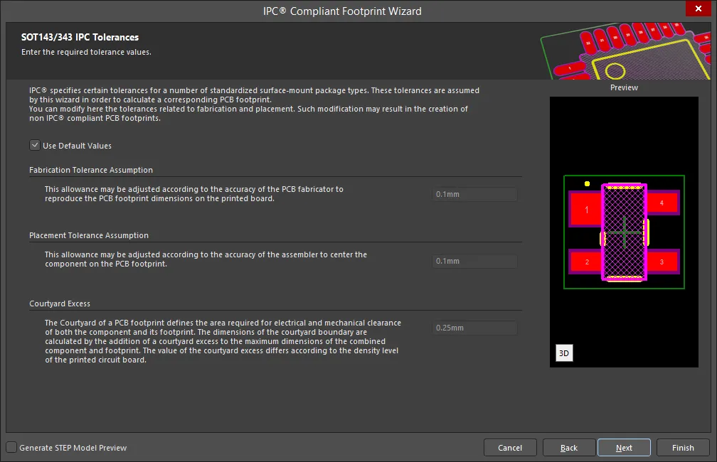
IPC specifies certain tolerances for a number of standardized surface-mount package types. These tolerances are assumed by the Wizard in order to calculate a corresponding PCB footprint. You can modify the tolerances related to fabrication and placement on the SOT143/343 IPC Tolerances page. Enable Use Default Values to accept the displayed values. You can change the values for Fabrication Tolerance Assumption, Placement Tolerance Assumption, and Courtyard Excess by entering the new values directly in the textboxes.
Modifying the IPC Tolerances may result in PCB footprints that are not IPC compliant.
SOT143/343 Footprint Dimensions
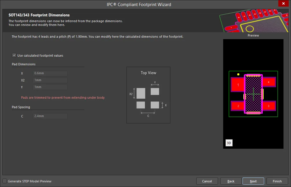
The SOT143/343 Footprint Dimensions page displays the inferred footprint dimensions using the package dimensions previously defined. To use the displayed values, enable Use calculated footprint values or enter new values for Pad Dimensions and Pad Spacing.
SOT143/343 Silkscreen Dimensions
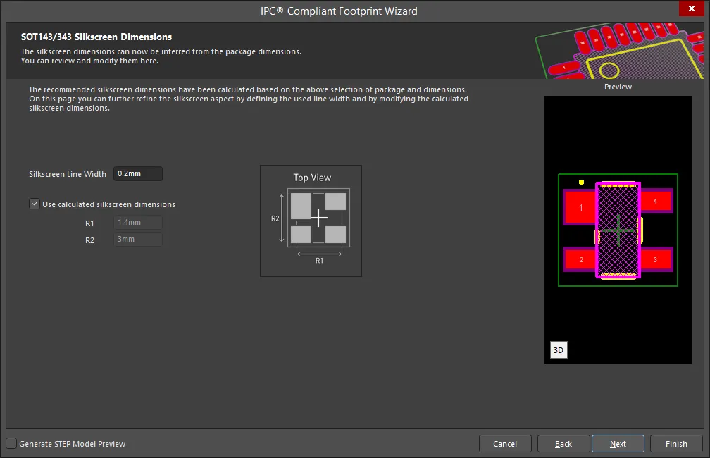
The SOT143/343 Silkscreen Dimensions page displays the inferred silkscreen dimensions using the package dimensions previously defined. You can further define the silkscreen dimensions by entering a new value for the Silkscreen Line Width. Enable Use calculated silkscreen dimensions to use the values displayed or disable the option and enter the desired values.
SOT143/343 Courtyard, Assembly and Component Body Information
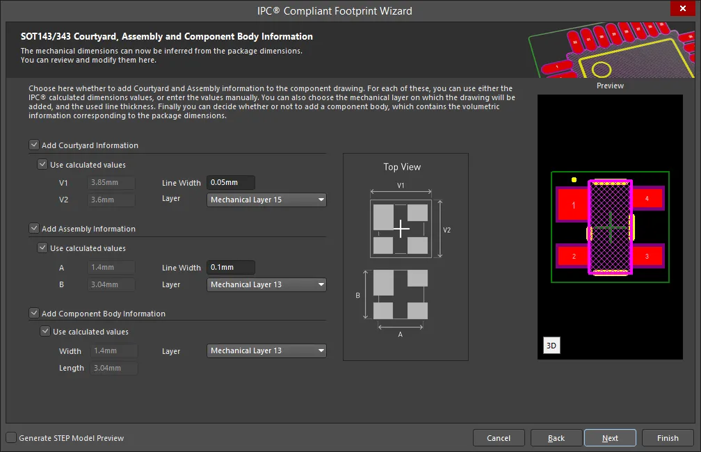
The SOT143/343 Courtyard, Assembly and Component Body Information page displays the inferred mechanical dimensions using the package dimensions previously defined.
Enable Add Courtyard Information and Add Assembly Information to add courtyard and assembly information to the component drawing. For each, you can use the IPC calculated dimensions or enter new values directly in the textboxes. If desired, enter a new Line Width directly in the textbox. You can also select the mechanical layer for courtyard and assembly by using the drop-down next to Layer and selecting the desired mechanical layer.
A component body contains the volumetric information corresponding to the package dimensions. Enable Add Component Body Information to include this information. Enable Use calculated values to use the values displayed or disable the option and enter new desired values. You can also select the mechanical layer for the component body by using the drop-down next to Layer and selecting the desired mechanical layer.
