Parent page: Working Between the Schematic and the Board
Whether you are transferring a captured design to a new PCB for the first time, or making changes to an existing design on either the schematic or PCB side, you need some way to keep the two sides in sync. Altium Designer includes powerful design synchronization capabilities that simplify the task of keeping the design synchronized, allowing the designer to keep their focus on the creative aspects of the design process.
 The synchronization process detects and resolves the schematic and PCB differences.
Design synchronization is performed directly between the schematic and PCB editors. The software uses a comparator engine to compare all aspects of the design, detailing the output as a list of differences. The designer decides which side should change to resolve the differences, and a set of Engineering Change Orders (ECOs) is created. These are then applied, bringing the two sides of the design back in sync.
There are two approaches to performing a synchronization:
- Bi-directional synchronization, where differences can be updated in both directions simultaneously, using the Project » Show Differences command (as shown above). Refer to the Finding Differences section to learn more about this approach.
- Single-direction synchronization, using the Design » Update PCB, or the Design » Update Schematic commands. Refer to the Performing a Direct Update section to learn more about this approach.
What Can be Synchronized?
The synchronization process ensures that the component and connective data on the schematic, matches the component and connective data on the PCB. As well as the component and connective data, the synchronization process also ensures that other design constraints; such as net classes, component classes and design rules, are also in sync.
Configuring the Comparator Options
Dialog page: Options for PCB Project, Comparator tab
Exactly what schematic and PCB data gets compared, is configured in the Comparator tab of the Options for PCB Project dialog. Select Project » Project Options to open the dialog.

The comparator engine obeys the settings defined in the Comparator tab of the Options for Project dialog.
The main region of the dialog includes a large list of Comparison Types, such as Different Designators and Changed Net Name, which are grouped in 5 categories. The Mode column on the right includes a dropdown for each, where you select the mode of comparison, such as Find Differences or Ignore Differences. Text-type comparisons have a third option, to allow the comparison to be case-insensitive.
The default for a new project is to Find Differences for every comparison type, set the options as required for your project.
- For schematic to PCB synchronization, all of the PCB related details can be synchronized.
- For PCB to schematic synchronization, only changes made to the component designator, comment and footprint can be synchronized back to the schematic. The only net changes that can be synchronized are changes due to a pin or part swap operation - how this is carried out depends on how the pin/part swap options are configured. To learn more, refer to the Pin and Part Swapping section.
Across the bottom of the dialog there are options for setting the Object Matching Criteria. Matching is a sophisticated, multi-pass process that does not rely on simple exact string matching. To learn more, refer to the Matching the Nets and Classes section.
Note the Ignore Rules Defined in the PCB Only option down the bottom of the dialog, enable this to exclude the rules you have defined in the PCB, from the comparison process.
Synchronizing Net and Component Classes
Dialog page: Options for PCB Project, Class Generation tab
As well as component and connective data, you can also generate and synchronize classes and design rules when you perform a Design » Update PCB. There are two types of classes that can be generated from the schematic and synchronized to the PCB:
- Automatic classes - derived from the buses/harness, components or sheet contents; and
- User-defined classes - derived from design directives placed by the designer.
The generation of these are configured in the Class Generation tab of the Options for Project dialog (the synchronization is controlled by options in the Comparator tab).
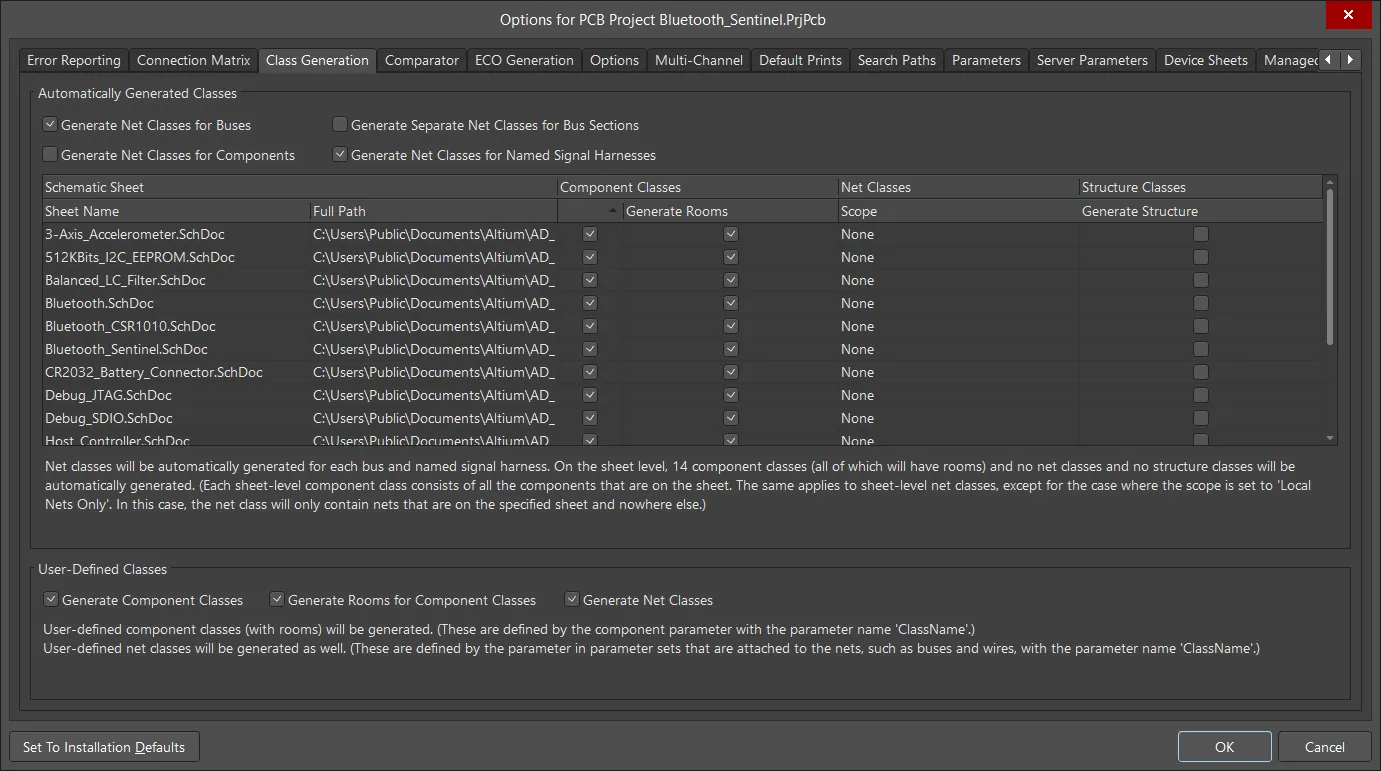
Use the options in the Class Generation tab to configure the automatically generated classes you require, and if you want to create user-defined classes during design synchronization.
Automatically Generated Net Classes
Net classes can be automatically generated for the following groups of nets:
| Named Signal Harnesses |
Signal harnesses are used to bundle and transport multiple nets across a schematic project. The harness is not used to name the nets carried within that harness, except when the harness has a net label placed on it. Note that placing a net label on a signal harness changes the net naming syntax, from being the individual net labels placed on the wires, to being <HarnessNetLabel>.<HarnessEntryName>. If you do not want to rename the nets in a harness, you can create a user-defined net class instead, as described below. Refer to the Working with Signal Harnesses section for more information about Signal Harnesses. Enable the Generate Net Classes for Named Signal Harness option to create a PCB net class for each named signal harness, during design synchronization. This is a global option that is applied to the entire project. |
| Buses / Bus Sections |
Enable the Generate Net Classes for Buses option to create a PCB net class for each bus (and each bus slice if the sub-option is enabled), during design synchronization. This is a global option that is applied to the entire project. |
| Components |
This option creates a net class for each component in the design, containing all of the nets connected to that component. This is a global option that is applied to the entire project. |
| Sheets |
Generate a net class for the nets within each sheet, as per the chosen scope. Note that Local Nets Only scope option will not include nets that enter or exit the sheet. Note also that a net can belong to more than one PCB net class, so the All Nets option will result in all of the sheet-spanning nets appearing in multiple classes. This option is configured for each schematic sheet. |
Automatically Generated Component Classes
It is common for the schematic project to be structured over multiple sheets, with each sheet representing a logical block of the overall design. Supporting this, you can automatically generate a component class that contains all of the components on that sheet, for each of the schematic sheets in the project, by enabling the appropriate Component Class checkbox. The PCB component class will have the same name as the Designator of the sheet symbol that references that schematic sheet. A component class will not be created if the sheet does not contain any components.
Automatically Generated Rooms
A room is a polygonal-shaped object that is an aid to component placement, these are created automatically for each schematic sheet that has the Generate Rooms checkbox enabled. In the PCB, each room is defined as a design rule, which will be created with the scope of InComponentClass('<SheetSymbolDesignator>'). A room will not be created if the sheet does not contain any components. When the schematic is initially transferred to the PCB, the components in each component class are arranged in a row, and then a room is created around that component class, as shown below.
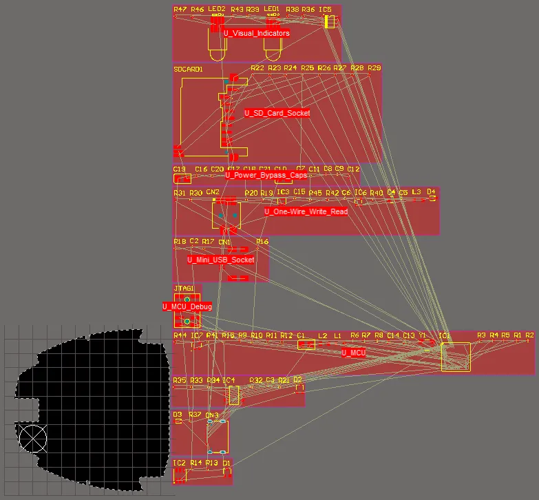
The PCB after initial design synchronization - a room has been created for each sheet, and that room has that sheet's component class assigned to it.
Automatically Generated Structure Classes
A structure class can include net classes, component classes, and lower-hierarchical-level structure classes, as its members. A structure class is created for each sheet that the option is enabled for, and will include the sheet-level component and net classes, if those options are enabled for that sheet. Edit the Structure Class in the PCB editor to add other net / component / structure classes. Use the Structure mode of the PCB panel to locate the components and nets in that structure class.
Creating User-Defined Classes
You can also create user-defined component classes and net classes, by attaching a parameter to the relevant component or net. PCB component and net classes will then be created if the appropriate User-Defined Classes checkboxes are enabled in the Class Generation tab of the Options for Project dialog.
User-Defined Component Class
In the schematic, you can specify that a component be added to a PCB component class when the schematic is synchronized with the PCB.
To do that, you add a parameter to the component, with the parameter Name string set to ClassName, and the parameter Value string set to the required <PCB_ComponentClassName>, as shown in the example image below. In this example, the entire section of circuitry was selected, and then in the Properties panel the object filter was set to only show components so the parameter could be added to all selected components in single edit action.
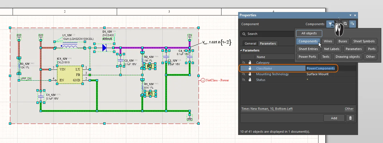
All of the selected components have had the parameter ClassName = PowerComponents added. Hover over the image to show this class of components on the PCB.
User-Defined Net Class
Object page: Parameter Set
To add a net (or the nets in a bus or signal harness) to a PCB net class, you need to attach a parameter to that net/ bus / harness. You do that by placing a Parameter Set object with its end touching the net / bus / harness, as shown in the image below (Place » Directives » Parameter Set command).
In the Classes section of the panel, enter the name of the net class, as shown in the image below.
Multiple Parameter Set objects can be placed in different locations on the schematic, to add multiple individual nets to the same PCB net class.

To add a net to a PCB net class, attach a Parameter Set object to the schematic net, then add a Class definition to the Parameter Set object.
Using a Blanket to Apply a Directive to Multiple Nets
Object page: Blanket
You can also add multiple nets to a PCB net class by placing a Blanket directive that covers all of those nets. The function of a Blanket is to allow you to apply a directive to all of the nets under the blanket (either identified by a net identifier, such as a Net Label or Power Port that is under the blanket, or a net that has an end vertex contained within the Blanket).
Instead of placing the Parameter Set directive so that it touches a wire, you place it so that it touches the edge of the blanket, as shown in the image below. Note that it is the value of the Parameter within the Parameter Set object that defines the PCB net class name, not the display name of the Parameter Set object. In the example image below, the Parameter Set is also used to define a routing width design rule.

Using a Blanket directive to bundle all the nets under it, into a PCB net class called Power. Note that the Parameter Set object name is not used for naming, it is a visual reference only.
A component / net can belong to multiple component / net classes in the PCB.
Synchronizing Design Rules
Design rules can be defined in the schematic, using a Parameter Set object. When a Parameter Set object is selected, the Properties panel includes a Rules region, click the Add button to add a design rule. The Rule will be applied to the net / bus / harness / objects under the blanket, that the Parameter Set object is touching.
In the image below, a width constraint design rule is being applied to the USB_data net class (the net class is also defined as part of this Parameter Set, in the Classes region of the panel).

The Parameter Set is used to define a net class and a design rule, to the nets under the schematic blanket object. Note that the required measurement units are configured at the bottom of the Edit PCB Rule dialog.
Adding a Design Rule in the schematic
- Attach a Parameter Set to the net / bus / harness / blanket (add a Net Class definition in the Parameter Set, if required).
- Add a Rule definition in the the Parameter Set. This will open the Choose Design Rule Type dialog, as shown above.
- Select the required Rule Type.
- Click the OK button to open the Edit PCB Rule dialog.
- Configure the PCB rule requirements as required. Note that the measurement units required for this PCB rule are selected at the bottom of the dialog.
In the Comparator tab of the Options for Project dialog, ensure that the required Rule type comparisons are enabled, to allow design rules to be added and updated in the PCB.
Each PCB rule that is created from a schematic rule definition is automatically named Schematic <RuleType>. If required, this name can be edited as it is not used for ongoing rule synchronization.
In both the image above and the image below, the design rule is defined in a Parameter Set object that is attached to a blanket. By including a Class definition in the Parameter Set object, a PCB net class will also be created, and because the class definition is present, the PCB rule will be scoped InNetClass('<PCB_NetClassName >').
In the image below you will notice that the Parameter Set object is displayed as a Differential Pair directive. This is a special type of Parameter Set object, placed using the Place » Directives » Differential Pair command.

The Differential Pair directive is used to define a net class and a design rule, which is then applied to targeted diff pairs.
Working with Differential Pairs
The Differential Pair directive is used to indicate nets that belong to a differential pair. The software requires the nets in the pair to be named <Name>_P and <Name>_N. The PCB differential pair will then be named <Name>.
Pairs can be defined by placing a Differential Pair directive on every differential pair member, or a blanket can be placed so that it covers the pair net names, as shown in the image above.
Referring to the image above, the differential pair Parameter Set object results in the creation of:
- Eight differential pairs, named
V_RX0, V_TX0, V_RX1, V_TX1, RX0, TX0, RX1, TX1.
- A PCB net class, called
ROCKET_IO_LINES.
- A
Differential Pairs Routing design rule, configured to target the PCB Net Class, ROCKET_IO_LINES.
Configuring the ECO Generation Options
The Options for Project dialog also includes an ECO Generation tab. This tab defines which design modifications can have ECOs created. Typically these are all enabled, with the options in the Comparator tab of the dialog being used to configure which design changes are to be synchronized between the schematic and the PCB.
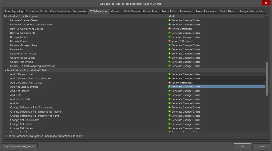
The ECO Generation tab defines which types of modifications can have ECOs created.
Finding Differences
The design synchronization feature is able to detect and resolve differences in both directions; that is, from the schematic to the PCB, or from the PCB back to the schematic.
There are two approaches to detecting and resolving differences:
- Assign the update direction for each change.
- Apply all updates in the same direction.
If you do not need to apply updates in both directions at the same time, then you do not need to go through the process of choosing the documents to compare and configuring the update direction for resolving the differences. In this case, you can go straight to the Performing a Direct Update section.
The software is capable of resolving these differences by applying changes to both sides, at the same time. For example, imagine the scenario where the electronics designer has changed the value of a capacitor, while the PCB designer has changed the footprint of that same capacitor. These two differences can be resolved in a single update process, by applying the comment change as a schematic-to-PCB update, and the footprint change as a PCB-to-schematic update.
When the comparator engine compares the schematic project to the PCB, a complete list of differences is created - at this stage there is no assumption on which side must be changed to bring them back into sync.
The list of differences can be seen in the Differences between dialog. To open the Difference between dialog and see a list of differences:
- Run the Project » Show Differences command to open the Choose Documents to Compare dialog, as shown in the image below. The Choose Documents to Compare dialog is used to select what two documents/document-sets you will be comparing, typically it is the schematic project against the PCB. You can also use this dialog to compare any document to any document by ticking the Advanced Mode option. For example, you might be comparing a netlist to a PCB, or a PCB to a PCB.
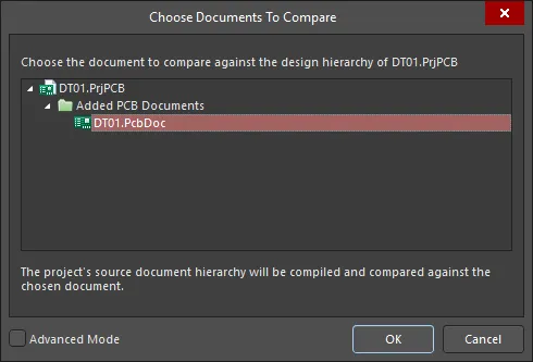
Select the PCB to compare the schematic project against.
- Select the PCB in the main part of the dialog, and click OK to open the Difference between dialog, as shown below.
The Differences between dialog will open. The next step is to assign an update direction to each difference:
- For an individual difference, click in the Update column to display a direction selector, as shown in the image below.
- For multiple differences of the same kind, right-click on a heading, such as Different Footprints, and select the required Update Same Kind command.
- For all differences, right-click anywhere in the dialog and select the required Update All command.

For each difference, the Update direction must be set for an ECO to be created to resolve that difference.
Once the Update direction has been assigned, click the Create Engineering Change Order button to open the Engineering Change Order dialog, which is described below.
Performing a Direct Update
Since the designer usually knows which way they want to apply the updates and those updates are all in the same direction, you can choose to skip the difference detection and direction assignment process that has just been described.
Rather than selecting the Show Differences command from the Project menu, you choose the Update command from the Design menu, from either the schematic editor or the PCB editor. Your choice of editor from which you run the command, indicates the direction you want the changes to be made - from this editor, to that editor. For example, you would choose Design » Update in the schematic editor to push all changes from the schematic to the PCB.
The Differences between dialog will be skipped and you will jump straight to the Engineering Change Order dialog.
 If all of the updates are going to be applied in the same direction, use the Design » Update command.
Resolving Differences - Applying the ECOs
Dialog page: Engineering Change Order
Each difference is resolved by applying an Engineering Change Order (ECO). The ECOs are listed in the Engineering Change Order dialog with one ECO per line, each with its own Enable checkbox.
When using the Engineering Change Order dialog:
- The dialog opens with all changes enabled, disable any changes you wish to hold off for now. The dialog supports multi-select - use the right-click context menu to toggle the enable state of selected ECOs.
- Use the right-click Cross Probe command to examine the objects affected by that ECO.
- Use the Validate Changes button to check that the changes can be performed. ECOs typically fail because an object is not available - for example, the specified PCB footprint does not exist in the Available File-based Libraries, or the specified pad does not exist on the footprint.
- An ECO can also fail because an object that is needed by a certain ECO was not present, but was added during the processing of the current ECOs. In this situation, run the Update command again to complete that ECO.
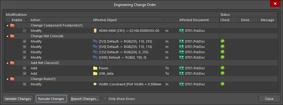
Each design change presents as an ECO, enable those that are required.
The ECO dialog supports multi-select. Right-click in the dialog to access commands to: Enable or Disable Selected ECOs, or to Cross Probe to objects affected by that ECO.
Understanding the Linking Between the Schematic and the PCB
Component Matching via Unique Identifiers
Each schematic component links to its PCB component through a Unique Identifier (UID). The UID is assigned when the schematic component is placed on the sheet, and this value is transferred to the PCB component when the design is transferred to the PCB editor.
This scheme would be adequate for a simple design, but is not capable of supporting a multi-channel design. In a multi-channel design, the same schematic component is repeated in each physical channel, which would mean the repeated PCB components would have the same UID. To cater for this, the UID for the PCB component is created by combining the UID of the parent Sheet Symbol with the UID of the schematic component. The syntax of the PCB UID changes slightly, depending on how the multi-channel design has been created.
For a multi-channel design created by placing multiple Sheet Symbols that all reference the same schematic sheet, then each Sheet Symbol can provide a unique ID, so the PCB UID has the format:
\SheetSymbolUID\SchComponentUID
For a multi-channel design created using the Repeat keyword, there is only 1 Sheet Symbol UID available, so the PCB UID also includes the ChannelIndex value, in the format:
\ChannelIndex+SheetSymbolUID\SchComponentUID
The UIDs are not displayed in panels and dialogs.
When the Components are not Linked
The advantage of using a UID to match the schematic and PCB components is that it allows the designators to become unsynchronized (perhaps by performing a PCB re-annotate a number of times), without any risk of the schematic and PCB becoming unsynchronizable.
If there is a component present on the schematic or the PCB that does not have a matching component (same UID) present in the other editor, the following will occur:
- If the extra component is only present in the source editor, an ECO to add the component to the target editor will be generated.
- If the extra component is only present in the target editor, an ECO to remove the extra component will be generated.
- When there are unmatched components present in both editors, the software needs instruction on how to deal with them, so the Failed to Match Unique Identifiers dialog opens.
 The Failed to Match Unique Identifiers dialog
The dialog buttons have the following options:
- Automatically Create Component Links - click this button if you know that the unmatched components already have matching designators. Using the component designators, the software will assign matching UIDs to these extra components. For components that can be matched by designator, any other property differences (such as unmatched parameters), will result in ECOs being generated. If there are components that cannot be matched by designator, ECOs to add/remove these will be generated (extra components present in the source editor to be added, extra components in the target editor to be removed).
- Manual Component Links - click this button if you know there are components that match, but do not know the status of their designators. The Edit Component Links dialog will open (described below), where you can manually select each source and target component and transfer them to the matched components list, assigning them matching UIDs. ECOs will then be generated to synchronize the designators (and any other unmatched component properties).
- Cancel - click this button to generate ECOs to add extra components that are present in the source editor and remove extra components from the target editor.
Manually Linking Components
The status of the component links can be checked and managed at any time, in the Edit Component Links dialog (PCB editor, Projects » Component Links command).
Summarizing the dialog features:
- Components that are unmatched are presented in the two Un-Matched Components columns on the left, components that share a matching UID are presented in the Matched Components region on the right of the dialog.
- The arrow buttons in the middle of the dialog are used to manually match (or un-match) selected components.
- The Add Pairs Matched By button and options down the bottom of the dialog are used to scan the list of currently unmatched components, and attempt to match them by the enabled properties (Designator, Comment, Footprint).
- When the Perform Update button is clicked, each newly matched PCB component is assigned the UID of its schematic counterpart.
- After using this dialog to perform manual component linking, it is good practice to check the synchronization state (run the Design » Update command).
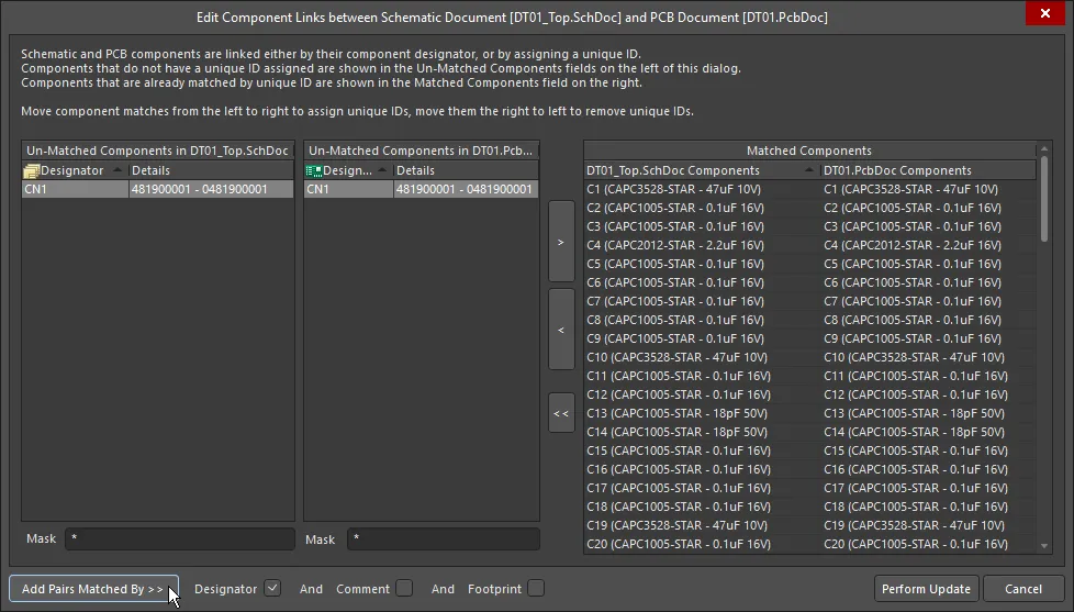
The Edit Component Links dialog is used to detect and resolve UID mismatches, it is run from the PCB editor.
If you copy/paste or cut/paste a schematic component, its UID is automatically renewed - this ensures that every component continues to have a unique identifier.
If you are reorganizing your schematic (which has already been transferred to the PCB editor) and need to move components to another sheet, don't cut/paste them, select them and run the Edit » Refactor » Move Selected Sub-circuit to Different Sheet command.
Matching the Nets and Classes
Both nets and classes have a parent (the net or class), and children (the members of that net or class). Matching these requires a different approach than the UID mechanism used for component linking, to support changes to: the parent; the children; or both the parent and its children. For example, something as simple as changing the name of a net on the schematic should not require that net and all its children pins be removed from the PCB, then the newly named net be added, and finally all the children pins be added to that new net.
To support this, the software includes separate matching algorithms to match nets and classes by their members, and also by their name. The matching process is configured in the Object Matching Criteria section of the Comparator tab of the Options for Project dialog.

The default settings is to match members first, then by Object Type name.
Matching for these types of objects is handled in the following way:
- During design synchronization, the default behavior is to first attempt to match by members, in accordance with the Min Match % and Min Match Member settings.
- If member matching fails, the software will then attempt to match by name (if the Use Name Matching option is enabled).
- If either of these matching processes succeeds, you will proceed to the Engineering Change Order dialog.
- If both matching techniques fail (or the Use Name Matching option is set to
Never), the Match Manually dialog will open.

- Clicking No in the Match Manually dialog will skip the user-matching process and jump straight to the Engineering Change Order dialog. Since you have not attempted to match any unmatched objects, the software assumes that the reference and target objects are unrelated, so ECOs will be generated that remove the Unmatched Reference Objects from the board, and add the Unmatched Target Objects as new objects.
- If you click Yes in the dialog to match manually, the Match dialog will open, as shown below (the dialog caption will change to suit the unmatched object type).

The Match dialog is used to manually match objects that you know to be matched. Leave the right side empty and click Continue if you are unsure.
- In this dialog, select the objects that you want matched in the Unmatched Reference Objects and Unmatched Target Objects, and then transfer them to the Matched Pairs section of the dialog. For these objects, the software will generate an ECO to update the names so they now match, and ECOs to remove/add members, so they also match.
- If you are unsure, you do not have to manually match objects. For any unmatched objects, the software assumes that the reference and target objects are unrelated, so will generate ECOs that remove the Unmatched Reference Objects from the board, and add the Unmatched Target Objects as new objects.
- Once you have matched those objects that you know do match, click Continue to open the Engineering Change Order dialog.
- If you click Cancel, the update process terminates.
Matching the Design Rules
Design rules that are defined on the schematic must also be linked to the matching rule on the PCB. If there was no linking mechanism, you would not be able to update the rule on the schematic and flow those changes to the PCB. UIDs are used to link the schematic design rule to the PCB design rule.
The UID is automatically assigned in the Parameter Set that holds the rule definition on the schematic, and transferred to the PCB during design design synchronization.
 Design rules use a UID to match the schematic design rule definition to the PCB design rule.
Typically, you will not need to manually manage the matching of rules, unless you have manually edited the UID in the PCB Rules and Constraints dialog in the PCB editor. If the UIDs do not match, the software will add a new rule to the PCB for any schematic rule that does not have a matching PCB rule, and remove any PCB design rule that does not have a matching schematic design rule.
You can freely update components in either editor and synchronize those changes to the other editor. Changes made to nets, classes, and rules can only be updated from the schematic to the PCB.