Silk to Solder Mask Clearance
Rule category: Manufacturing
Rule classification: Binary
Summary
This rule checks the clearance between any silkscreen primitive and any solder mask primitive or exposed copper-layer primitive (exposed through openings in the solder mask). The check ensures that the distance is equal to or greater than the value specified in the constraint.
Many manufacturers routinely strip (or 'clip') silkscreen to the mask opening and not just to the copper pad. However, doing so can render silkscreen text unreadable. Being able to catch such occurrences through DRC allows you to manipulate offending silkscreen text prior to sending the board to manufacturing.
Constraints
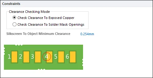
 Default constraints for the Silk To Solder Mask Clearance rule.
-
Clearance Checking Mode - choose a checking mode for the clearance:
- Check Clearance To Exposed Copper - in this mode, clearance checking is between silkscreen (Top/Bottom Overlay layer) objects and copper in component pads, which is exposed through openings in the solder mask.
- Check Clearance To Solder Mask Openings - in this mode, clearance checking is between silkscreen (Top/Bottom Overlay layer) objects and solder mask openings created by objects that include a solder mask, such as pads, vias, or copper objects with the Solder Mask Expansion option enabled.
- Silkscreen To Object Minimum Clearance - specifies the minimum permissable clearance between a silkscreen object and either exposed copper or solder mask openings, depending on the clearance checking mode chosen.
How Duplicate Rule Contentions are Resolved
All rules are resolved by the priority setting. The system goes through the rules from highest to lowest priority and picks the first one whose scope expressions match the object(s) being checked.
Rule Application
Online DRC and Batch DRC.
