Parent page: Tutorial - A Complete Design Walkthrough with Altium Designer
Main page: Defining Design Requirements Using the Constraint Manager
Do I have the Constraint Manager?
Altium Designer suggests two distinct approaches to defining design constraints: the PCB Rule and Constraints Editor dialog and the Constraint Manager. The Constraint Manager is available in a PCB design project only if the Constraint Manager functionality was available at the moment of creating that project (provided you have the System.ConstraintManager option enabled in the Advanced Settings dialog).
Note that this page applies only if the Constraint Manager is available. To quickly check if the Constraint Manager is available for the tutorial project, open the Design main menu from the Schematic editor when the project's schematic document is open and check for the Constraint Manager command.
If the Constraint Manager is unavailable, skip this tutorial page and go to the next page: Creating and Configuring the PCB Document.
Altium Designer's PCB editor is a rules-driven environment, meaning that as you perform actions that change the design, such as placing tracks, moving components, or autorouting the board, the software monitors each action and checks to see if the design still complies with the design constraints. If it does not, then the error is immediately highlighted as a violation. Setting up the design constraints before you start working on the board allows you to remain focused on the task of designing, confident in the knowledge that any design errors will immediately be flagged for your attention.
Design constraints are configured in the
Constraint Manager (
Design » Constraint Manager)
accessible from both the schematic and PCB sides of the design. In this tutorial, the design constraints will be defined from the schematic side and then transferred to the PCB, along with other design data (components and nets).
All design requirements are configured as constraints in the Constraint Manager.
Defining the Clearance Constraint
The first step is to define how close electrical objects that belong to different nets can be to each other.
This requirement is handled by the clearance design constraints. The Constraint Manager includes the Clearances view that presents the clearance matrix where clearances between net classes in the design can be defined. For the tutorial, a clearance of 0.25mm between all objects is suitable.
Note that entering a value into a cell in the clearance matrix or into the Clearance field will automatically apply that value to all of the fields in the grid region at the bottom of the Constraint Manager when a cell in the clearance matrix is selected. You only need to edit in the grid region when you need to define a clearance based on the object type.
Defining the Clearance Constraint
-
When the schematic sheet is the active document, select the
Design » Constraint Manager
command from the main menus to open the Constraint Manager. The Clearances view of the Constraint Manager opens by default.
-
Select the Tools » Measurement Units » mm command from the main menus to switch the current measurement units from mils to millimeters in the Constraint Manager.
-
Click within the cell on the intersection of the All Net Classes row and the All Net Classes column.
-
Type 0.25 in the Clearance field that appears in the bottom-left part of the Constraint Manager.

It is not necessary to enter the measurement units. The default measurement units will be added to the entered value automatically.
Defining the Width Constraints
The width of the routing is controlled by the applicable width design constraint, which is automatically selected when you run the Interactive Routing command and click on a net.
When you are configuring the constraints, the basic approach is to set the generic constraint to target the largest number of nets and then add specific constraints to target nets with special width requirements, such as power nets. Constraint priority applies automatically based on the natural hierarchy of design objects.
For example, the tutorial design includes a number of signal nets and two power nets. The net constraint for all nets can be configured at 0.25mm. Even though the All Nets scope also targets the power nets, these nets can be specifically targeted by adding a specific constraint.
-
The width design constraint includes Min, Max, and Preferred settings. Use these if you prefer to have some flexibility during routing, for example, when you need to neck a route down in a tight area of the board. This can be done on the fly as you route by pressing 3 to cycle through the routing widths. There are also other techniques for editing the routing width; these are discussed more in the routing section.
-
Avoid using the Min and Max settings to define a single rule to suit all sizes required in the entire design. Doing this means you forgo the ability to get Altium Designer to monitor that each design object is appropriately sized for its task.
Defining the Width Constraints
-
Open the Physical view of the Constraint Manager using the corresponding button at the top.
-
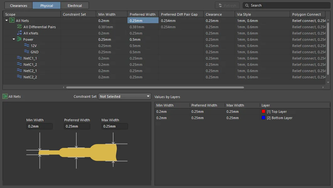
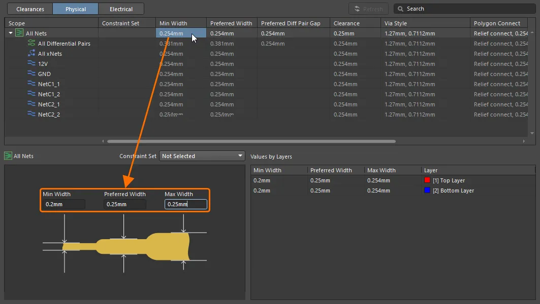
Click within the cell in the Min Width or Preferred Width column for All Nets.
-
At the bottom part of the Constraint Manager, define the following width values: Min Width = 0.2, Preferred Width = 0.25, Max Width = 0.25.
-
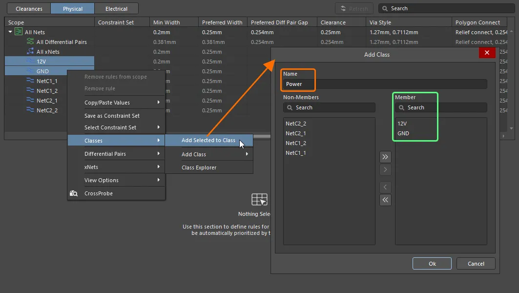
The next step is to add another constraint to specify the routing width for the power nets. To do this, let's create a net class for power nets and apply specific width constraints to this class. In the Physical view, select the rows for
12V and GND nets by holding the Ctrl key and clicking the net names, right-click the selection, and choose the Classes » Add Selected to Class command from the context menu.
-
In the Add Class dialog that opens, enter Power in the Name field, make sure that both 12V and GND nets are listed in the Member column, and click Ok.
-
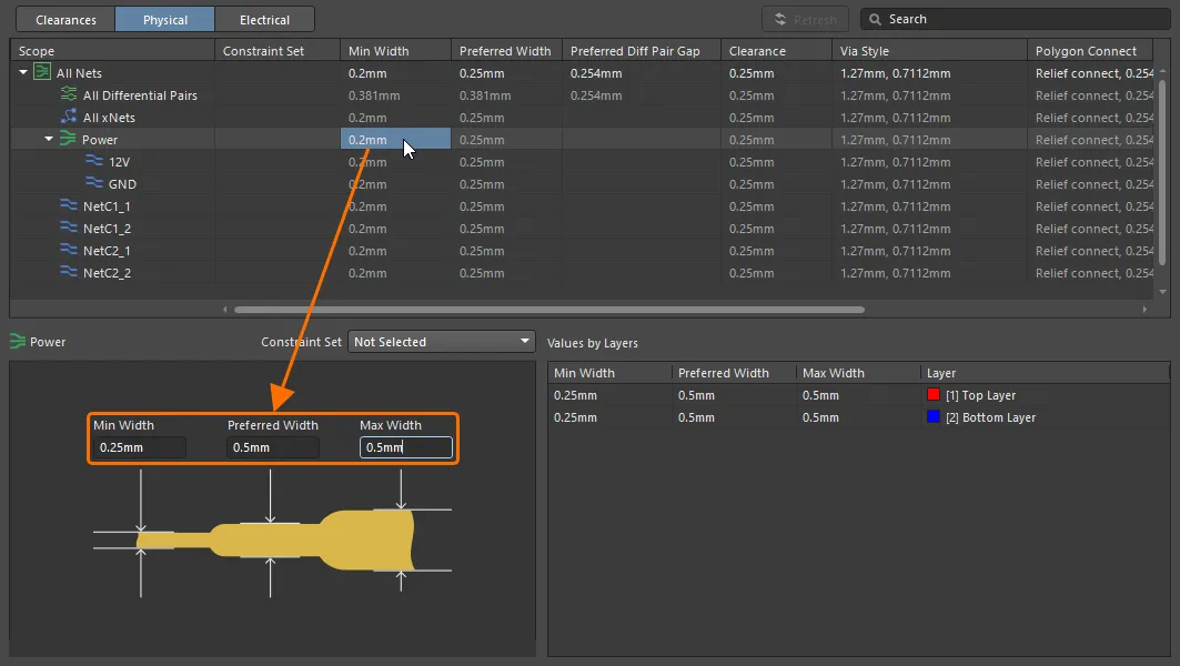
The Power net class entry will appear in the Physical view, with the 12V and GND nets listed under it. Click within the cell in the Min Width or Preferred Width column for the Power net class and define the following width values: Min Width = 0.25, Preferred Width = 0.5, Max Width = 0.5.
Defining the Via Style Constraint
As you route and change layers, a via is automatically added. In this situation, the via properties are defined by the applicable via style design constraint. If you place a via from the Place menu, its values are defined by the default primitive settings. For the tutorial, you will configure the via style design constraint.
Defining the Via Style Constraint
-
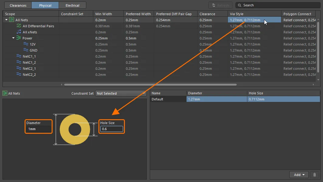
In the Physical view of the Constraint Manager, click within the cell in the Via Style column for All Nets.
-
Since it is highly likely that the power nets can be routed on a single side of the board, it is not necessary to define a routing via style rule for signal nets and another routing via style rule for power nets. At the bottom part of the Constraint Manager, define the following via style values: Diameter = 1 and Hole Size = 0.6.
-
Save changes in the Constraint Manager (File » Save) and close it (right-click the document tab of the Constraint Manager and select the Close Multivibrator.PrjPcb [Constraints] command from the context menu).
Defining the constraints is now complete. It's time to
create the PCB!
