Main page: Preparing Your Design for Manufacture
Now that you've completed the design and layout of the PCB, you're ready to produce the output documentation needed to get the board reviewed, fabricated, and assembled.
Because a variety of technologies and methods exist in PCB manufacture, Altium Designer has the ability to produce numerous output types for different purposes, including Gerber files, ODB++ files, Pick and Place files, Bill of Material reports, PDF 3D, etc.
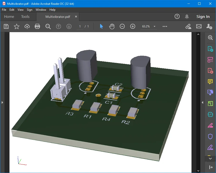
Output types include PDF 3D, with full zoom, pan and rotate, and the ability to control the display of nets, components, and the silkscreen, in Adobe Acrobat Reader®.
Adding an Output Job File to the Project
Main page: Preparing Manufacturing Data with Output Jobs
While you can selectively generate the required outputs from specific editors (e.g., using commands in the Fabrication Outputs and Assembly Outputs sub-menus of the File main menu in the PCB editor), Altium Designer provides support for Output Job files. An Output Job file (or 'OutJob' for short) stores settings for each output type. An OutJob allows you to configure each output type, configure their output naming, format, and output location. Outputs can be generated from an OutJob directly or as a part of the integrated project release process.
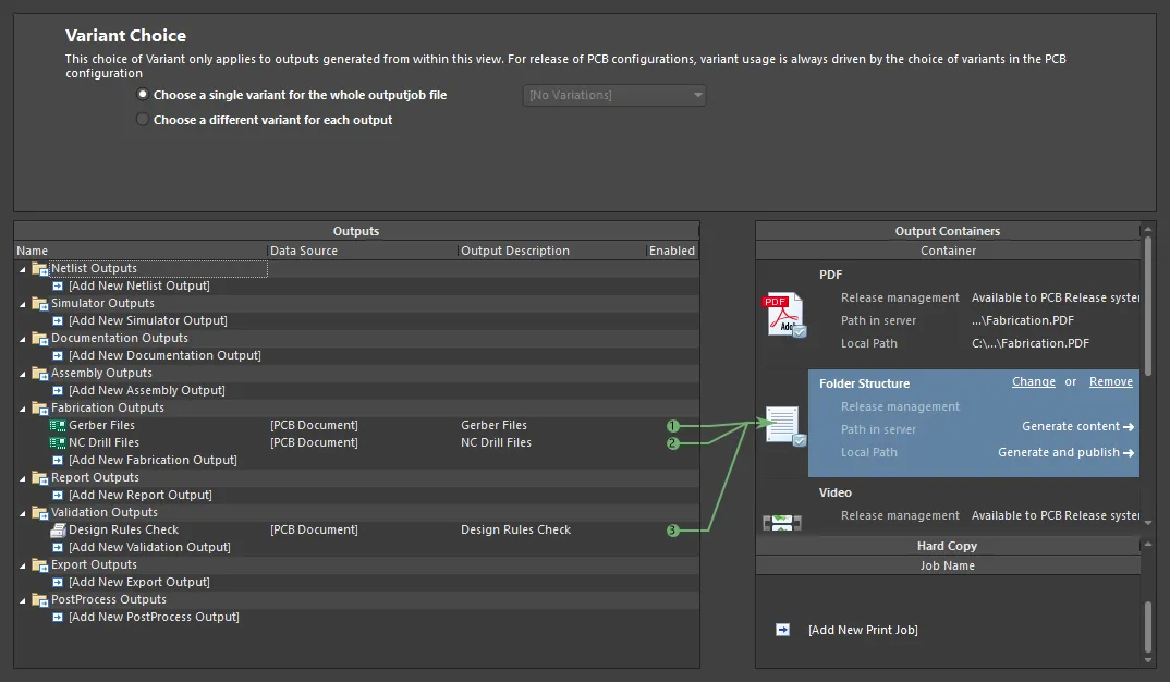
An Output Job file allows you to configure each output type, configure their output naming, format, and output location. Output Job files can also be copied from one project to another.
Adding an Output Job to the project
The OutputJob file, or OutJob, maps each output (in the list on the left) to an output container (in the column on the right). The output setting defines what you want to output (double-click to configure); the container defines where the output is to be written to (double-click the icon, or click the Change link). Any number of outputs can be added in the OutJob, and outputs can be mapped to individual or shared output containers.
-
In the Projects panel, right-click on the project name and select Add New to Project » Output Job File. A new OutJob will be opened and added to the project.
-
Save the OutJob and name it Fabrication. It will automatically be saved in the same folder as the project file.
-
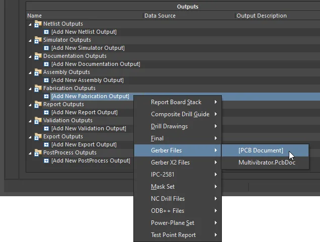
To add a new Gerber output, click the Add New Fabrication Output link in the Fabrication Outputs section of the OutJob and select Gerber Files » [PCB Document] as shown in the image below. If you select the [PCB Document] option, the project PCB is automatically chosen. Choosing this also means the OutJob can easily be copied between projects, as this setting will not have to be updated. If there are multiple PCBs in the project, you will need to select the specific board.
-
The Gerber output has been added; you will configure it shortly.
Configuring the Gerber Files
Main page: Preparing Fabrication Data
-
Gerber continues to be the most common form of data transfer between board design and board fabrication, with Gerber X2 and ODB++ becoming more and more popular.
-
Each Gerber file corresponds to one layer of the physical board: the component overlay, top signal layer, bottom signal layer, top solder mask layer, and so on. It is advisable to consult with your board fabricator to confirm their requirements before supplying the output files required to fabricate your design.
-
If the board has holes, an NC Drill file must also be generated, using the same units, resolution, and position on film settings.
-
Gerber files are configured in the Gerber Setup dialog, accessed via the PCB Editor's File » Fabrication Outputs » Gerber Files command, or by adding a Gerber output into the Fabrication Outputs section of an Output Job then double-clicking on it.
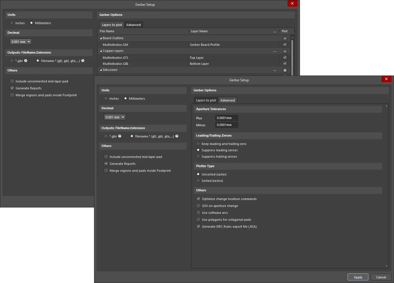
Configure the Gerber outputs in the Gerber Setup dialog.
Configuring fabrication outputs generation
-
In the OutJob, double-click on the Gerber Files output added in the previous set of steps. The Gerber Setup dialog will open, as shown in the image above.
-
Since the board has been designed in Metric, make sure that the Units are set to Millimeters in the dialog.
-
The smallest unit used on the board is 0.25mm for the routing and clearance, but because most of the components have their reference point at their geometric center (and were placed on a 1mm grid), some of their pads will actually be on a 0.01 grid. Set the Decimal option to 0.001 mm. This ensures that the resolution of the output data is more than adequate to cover these grid locations.
-
Click the Plot Layers button at the bottom of the Layer to plot tab and choose Select Used.
-
Click Apply to accept the other default settings and close the Gerber Setup dialog.
-
Same way, add the NC Drill output to the OutJob file – click the Add New Fabrication Output link in the Fabrication Outputs section of the OutJob and select NC Drill Files » [PCB Document].
-
Double-click on the added NC Drill Files output to access the NC Drill Setup dialog. Set the Units to Millimeters and the Format to 4:3. Make sure that the Coordinate Position option is set to Reference to relative origin, and click OK to accept the other default settings and close the dialog.
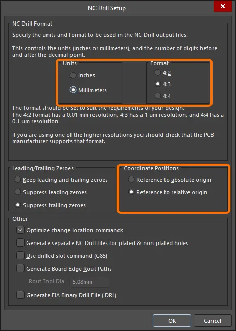
The NC Drill Setup dialog configured to generate proper NC Drill files for the tutorial
The NC drill file must always be configured to use the same Units and Format settings as the Gerber files otherwise the drill locations will not match the pad locations!
-
Now that the Gerber and NC Drill settings are configured, the next step is to configure their naming and output location. This is done by mapping them to an Output Container on the right side of the OutJob. For discrete files with their own file format, use a Folder Structure container. Select Folder Structure in the list of Output Containers then click the radio buttons for the Gerber and NC Drill Files in the Enabled column of the Outputs section to map these outputs to the selected container, as shown below.

The OutJob configured to generate Gerber and NC Drill outputs as discrete files.
-
The last step is to configure the container. To do this, click the Change link in the container to open the Folder Structure settings dialog. Across the top are a set of controls that are used to configure if the outputs are Release Managed or Manually Managed; make sure that they are set to Release Managed. Explore the other options. The lower part of the dialog will display how the names and folder structure change as you select different options.
-
Click OK to close the dialog.
Configuring Validation Report Generation
Main page: Preparing Validation Reports
The software includes a number of validation checks, which can be included as an output, during output generation. Each produces an HTML report file. During the project release process, these checks will be performed prior generation of other outputs, and if any validation checks are not passed successfully, the release will fail.
Configuring Validation Report generation
-
To add a new Validation output, click the
 link in the Validation Outputs section of the OutJob and select Design Rules Check » [PCB Document].
-
Map the added report to the Folder Structure Output Container – select the Folder Structure container in the list on the right side of the OutJob, then click the radio button for the Design Rules Check output in the Enabled column of the Outputs section.
-
Save locally and close the OutputJob file.
Preparing the Output BOM
Main page: BOM Configuration in the Report Manager
The actual output BOM file that is generated is done using the Report Manager. The Report Manager is a highly configurable report generation engine that can generate output in a variety of formats including text, CSV, PDF, HTML, and Excel. Excel-format BOMs can also have a template applied using one of the pre-defined templates or one of your own. An Excel-format BOM can also be generated without Microsoft Excel being installed; select the MS Excel File option in the File Format drop-down.
-
The Report Manager generates BOM output from the Bill of Materials For Project dialog, accessed via:
-
The schematic or PCB editor's Reports » Bill of Materials, or
-
By adding a BomDoc to the project and running the BomDoc's Reports » Bill of Materials command, or
-
By adding a Bill of Materials into the Report Outputs section of an Output Job.
-
The default behavior is for the Report Manager to present the component detail in the same way it has been configured in the BomDoc if the project includes a BomDoc. Columns can be added and removed using the Columns tab in the Properties region of the dialog.
-
If the project does not include a BomDoc, the Columns tab includes an additional region, used to define how like-components are identified for clustering. Clustering is achieved by dragging and dropping component attributes to the Drag a column to group region of the dialog.
-
The main grid region of the dialog is the content that is written into the BOM. In this region, you can click and drag to reorder the columns, click on a column heading to sort by that column, Ctrl+Click to sub-sort by that column, and define value-based filters for a column using the small drop-down in each column header.
-
By default, the BOM generator sources information from the schematic documents. A variety of Sources are available. Use the buttons in the Columns tab in the Properties region of the dialog to enable other sources. For example, if you enable the PCB Parameters you can include detail such as component location and side of board if required.
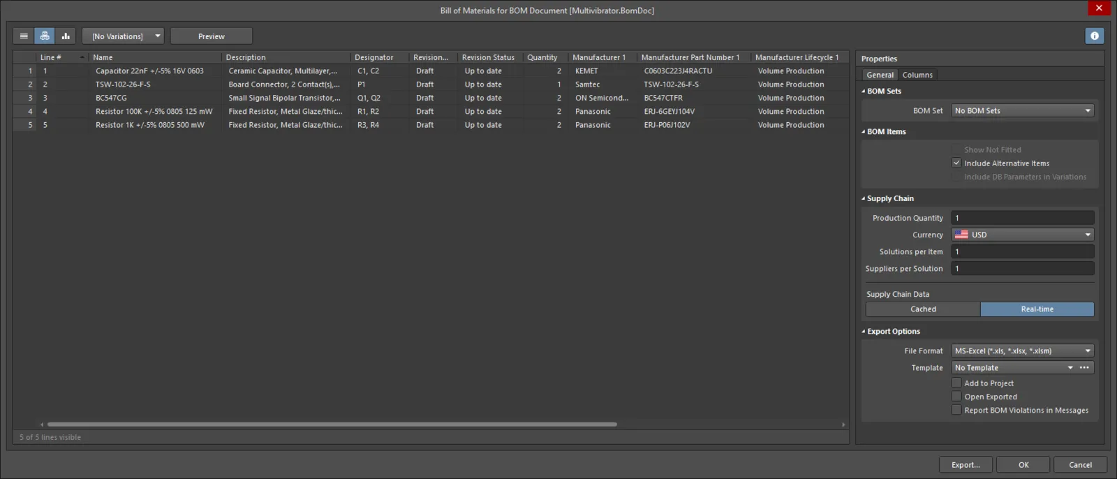
The Report Manager takes the configuration from the BomDoc if the project includes a BomDoc.
Mapping Design Data into the Generated BOM
Design data can be passed from Altium Designer into an Excel-format Bill Of Materials by referencing an Excel template that includes special statements.
When creating the Bill of Materials template in Excel, a combination of Fields and Columns can be used to specify the desired layout. Several example templates are included with the software in the \Templates folder of the installation user files. Refer to the Mapping Design Data into the BOM section of the BOM Configuration in the Report Manager page for details of the available fields. Note that fields need to be defined above or below the Column region of the template.
Configuring assembly outputs generation
-
Add a new OutJob file to the project and save it as
Assembly in the same folder as the project file.
-
To add a new BOM output, click the Add New Report Output link in the Report Outputs section of the OutJob and select Bill of Materials » [ActiveBOM Document].
-
Double-click on the added Bill of Materials output to open the Report Manager dialog.
-
In the Export Options of the Properties pane on the right side of the dialog, set Generic XLS (*.xls, *.xlsx, *.xlsm) for the File Format and BOM Template Single Supplier for the Template.
Unlike the MS-Excel (*.xls, *.xlsx *.xlsm) file format, Generic XLS (*.xls, *.xlsx, *.xlsm) uses a built-in XLS-format file generator, so that this format can be generated without having Microsoft Excel installed.
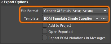
The Report Manager takes the configuration from the BomDoc if the project includes a BomDoc.
-
Click OK to save changes and close the dialog.
-
Add a new Draftsman output by clicking the Add New Documentation Output link in the Documentation Outputs section of the OutJob and selecting Draftsman » All Draftsman Documents.
-
In the OutJob file, map the added BOM report and Draftsman document to the PDF Output Container – select the PDF container in the list on the right side of the OutJob, then click the radio buttons for the Bill of Materials and Draftsman outputs in the Enabled column of the Outputs section.
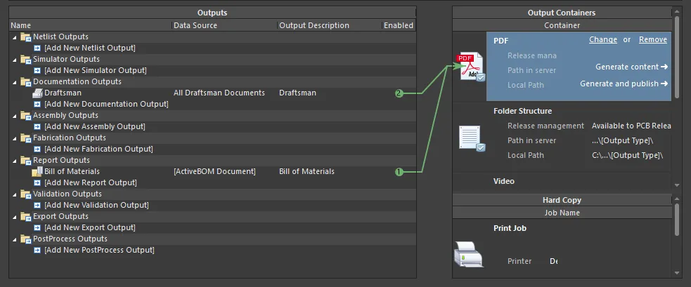
-
Configure the PDF container – click the Change link in the container to open the PDF settings dialog. Click the Assembly.PDF entry, select the Separate file for each output using output name, and click Done. The output BOM will be assigned the name set to the output in the OutJob file (Bill of Materials.pdf), that can be seen in the Preview region of the dialog.

Configure the BOM output naming in the PDF setting dialog.
-
Click OK to close the dialog.
-
Add the Pick & Place output to the OutJob file – click the Add New Assembly Output link in the Assembly Outputs section of the OutJob and select Generates pick and place files » [PCB Document].
-
Double-click on the added Generates pick and place files output to access the Pick and Place Setup dialog. Set the Units to Metric in the Output Setting region on the bottom left part of the dialog and click OK to accept the other default settings and close the dialog.
-
Map the added Pick & Place output to the Folder Structure Output Container – select the Folder Structure container in the list on the right side of the OutJob, then click the radio button for the Generates pick and place files output in the Enabled column of the Outputs section.
-
Save the OutJob file and the project locally.
Project Release
Main page: Design Project Release
With output documentation configured in OutJob files, the project is ready to be released to the connected Workspace. The board design release process is automated, enabling you to release your board design projects without the risks associated with manual release procedures. When a particular project is released, a snapshot of the design source is taken and archived along with any generated output – which represents a tangible product that is made from that design project and sold by the company.
The release process itself is performed using Altium Designer's Project Releaser, the user interface to which is provided courtesy of a dedicated view – the Release view. The release process is a staged flow, with the entries on the left-hand side of the view showing you at-a-glance, which stage you are currently at.
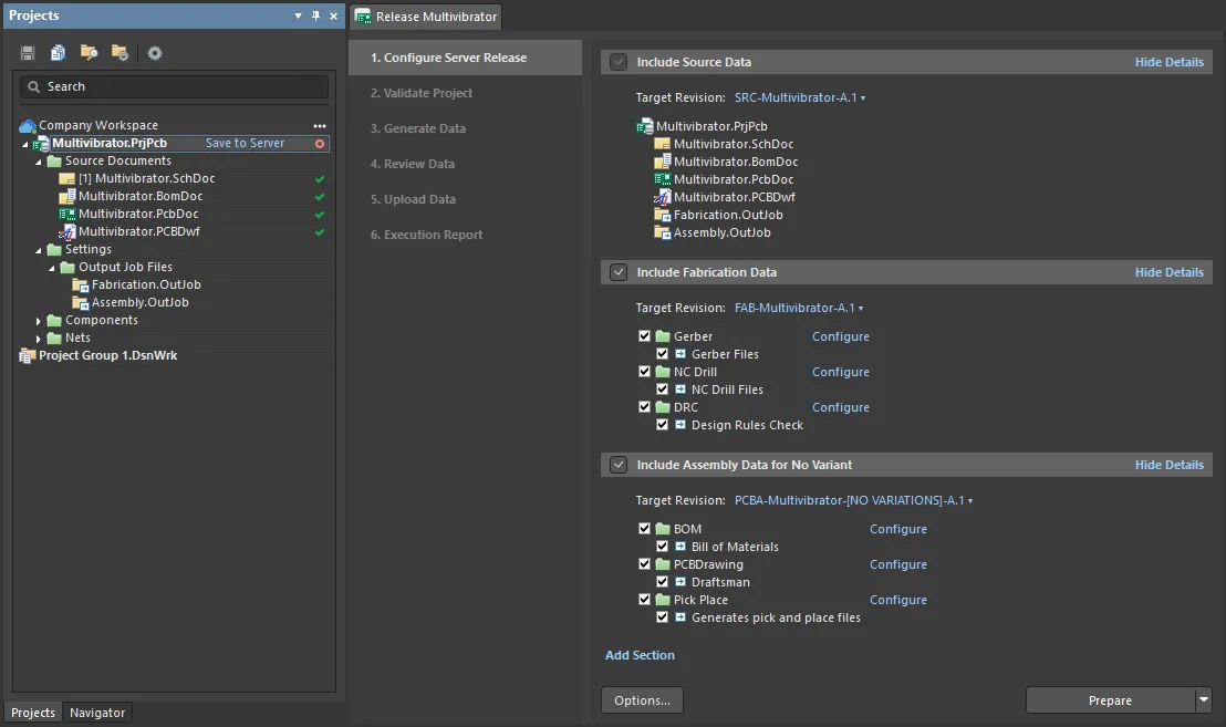
The Release view – the user interface to the Project Releaser.
Releasing the project
-
Access the Release view – right-click the project file in the Project panel and select the Project Releaser command from the context menu.
-
The Release view will open as a separate document tab. In the first stage – 1. Configure Server Release (shown in the image above) – you specify the type(s) of data that you wish to generate. Click on Details controls at the far right of each data set header to access details of what exactly is going to be generated by a data set.
-
Click the Options button at the bottom-left of the view to access the Project Release Options dialog. On the dialog's Release Options tab, make sure that the Managed - <WorkspaceName> is selected as the Release Target; Fabrication is assigned to Fabrication Data set, and Assembly is assigned to the Assembly Data set. Click OK to close the dialog and get back to the Release view.
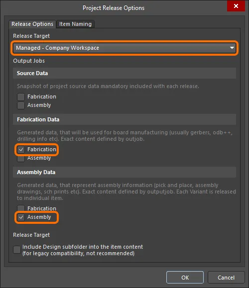
Configure options for the online release in the Project Release Options dialog.
-
Make sure that both fabrication and assembly Data Items are included in the release – Include Fabrication Data and Include Assembly Data for No Variant options are enabled (source data are always included in the project release) – then click the Prepare button to proceed.
-
The Item Creation dialog will open, with the list of target release items to be created in the Workspace. Select the Create items option to confirm creation of the items.
-
The Project Modified dialog may open. In this case, select the Save and Commit changes option to save the changes locally and proceed with saving the changes to the Workspace.
If there are changes to the project and/or its files that have not been saved to the Workspace yet, the Pending Commits dialog will open, alerting about this fact. Select the Commit option to proceed with saving the changes to the Workspace.
-
In the Commit to Version Control dialog that opens, make sure that modified project's source files, and those that are not in version control, are enabled, enter a meaningful Comment (e.g., The project is ready for release), and click the Commit And Push button.
-
The next stage of the release process – 2. Validate Project – is run automatically when one or more Validation-type reports are detected in assigned OutJob file(s). As the Fabrication OutJob file includes generation of the Desing Rules Check report, this validation output generator is run.
If any validation checks are not passed successfully, the release will fail. For the project release in this tutorial, this will mean that the PCB document includes at least one DRC violation. In this case, stop the release process with the Cancel button at the bottom-right of the view, open the PCB document, resolve the DRC violations, then start the release process again.
-
If validation is successful, the next stage of the release process – 3. Generate Data – is run automatically. This is where all other outputs – defined in the OutJob file(s) assigned to the included Data Items – are run, to generate the data to be released into the relevant target items in the Workspace.
-
With all validation checks passed, and output data generated, the next stage of the release process – 4. Review Data – allows you to review the generated data. Click a View link to open the associated data file, or file set, either within the relevant editor within Altium Designer (e.g., the CAM editor) or within the relevant external application (e.g. a PDF viewing tool). If the generated data all looks good, proceed with the release by clicking the Release button at the bottom-right of the view.

Review of the generated data, ready to be released to the Workspace.
-
The Confirm Release dialog will open, summarizing the configurations of the project that will be released to the Workspace. Enter a Release Note (e.g., Initial Release), and click OK.
-
After confirming the release in the previous stage, the next stage – 5. Upload Data – is automatically entered. It simply presents the progress of data upload into the revisions of the relevant data Items in the Workspace.
-
The final stage of the process – 6. Execution Report – provides a summary of the release. Close the Release view using the Close button at the bottom-right of the view.
You started with a blank schematic sheet and worked through to a finished PCB with output files released to the Workspace, which is the entire design process in Altium Designer. Next, we will explore some features related to
project management and collaboration.
