For the latest DC Power Integrity analysis functionality, take a look at Altium's Power Analyzer by Keysight - supported for use in Altium Designer 22.10 and later.
The practical performance of a PCB design layout depends on a multitude of factors, many of which can be predicted, to a reasonable degree, through a range of PCB design analysis tools such as post-layout Signal Integrity analysis. What's often neglected, however, or simply relegated to a 'rule of thumb' methodology, is developing the most effective layout design for board's DC Power Delivery systems. This is the judgment applied to the design of a board's copper areas that provide both the DC supply rails to the circuitry and their ground or common return path to the DC supply source. The desired outcome is an efficient design that maintains the integrity of the design's DC power layout.
With modern digital designs featuring high-speed circuitry, multiple devices, densely populated boards, and multiple supply rails, the demands placed on a design's DC power distribution network warrants a more analytical approach to its design. The DC analysis of a Power Delivery Network (PDN), or the results of its DC Power Integrity (PI-DC), is basically aimed at ensuring that adequate copper has been provided in the path from the voltage sources to the loads – in other words, that the planes, traces, and vias on the board are of sufficient size (and characteristics) to meet the power consumption requirements of the devices on the board.
Fortunately, the guesswork can be removed from the assessment of a PCB's power delivery network (PDN) through the use of a DC Power Integrity (PI-DC) simulation tool, which analyzes a board design's DC performance based on its electrical and physical properties. Such a tool is now available for Altium Designer as the Altium PDN Analyzer powered by CST® (Computer Simulation Technology).
Provided as a downloadable Altium Extension application, the PDN Analyzer integrates directly with Altium Designer to allow PI-DC simulation and analysis of the current PCB project. Since the PDN Analyzer functions within Altium Designer there are no manual data import/export requirements, data conversions or separate applications to be run – simply start the PDN Analyzer from the Schematic or PCB editor, set the desired test parameters and run the simulation. The results are primarily delivered through 2D/3D modeling of the circuit board copper layout, allowing a quick assessment of the results and the opportunity to perform exploratory 'what if' testing of the PCB layout design.

The PDN Analyzer interface shown with the Altium Designer Spirit Level example PCB, and the results of a PI-DC Voltage Drop simulation of its Top layer GND net return for the VCCINT supply.
► See information on Installing and Licensing the PDN Analyzer extension.
PDN Analyzer Version 2.0
First released as PDN Analyzer version 1.x, the significantly revised PDN Analyzer version 2.0 offers a redesigned interface, new features and more comprehensive results reporting.
The PDN Analyzer 2.0 extension is available for Altium Designer 17.1 and later.
Release Notes for PDN Analyzer 2.0
Version 2.0.2
Builds: 306 (for Altium Designer 17.1), 307 (for Altium Designer 18.0) and 309 (for Altium Designer 18.1)
Improvements:
| 22509 |
Improved current density uniformity at shape boundaries. |
| 24918 |
Enabled docking of the PDN Analyzer panel by default. |
| 24934 |
Reduced the default width of the simulation pane. |
| 24938 |
Added batch analysis confirmation window. |
| 24972 |
Allow a config to be opened after its PCB design was renamed. |
| 24993 |
Improved network rendering for more complex topologies. |
| 25188 |
Improved Highlight Peak Value "In View" mode behavior. |
| 25189 |
Aligned Probe X, Y coordinates units with AD units. |
Bug Fixes:
| 24523 |
Corrected via mesh data for current density. |
| 24636 |
Fixed bug related to layout changes not propagating to PDNA. |
| 24639 |
Corrected engineering notation representation of some numerical results. |
| 24649 |
Corrected Settings form window height. |
| 24662 |
Corrected HTML report least margins results. |
| 24664 |
Changed certain HTML report results representation to engineering notation. |
| 24665 |
Auto-close HTML Report generation window. |
| 24911 |
Fixed ODB++ export for pads with offset holes. |
| 24913 |
Fixed bug that reported a VRM's max pin current in the max power column. |
| 24914 |
Fixed bug in a selection of the bottom item in DC Nets list. |
| 24941 |
Corrected erroneous HTML report classification of Prepreg layers as Core. |
| 24944 |
Fixed a bug that limited the number of sequential VRMs to 1. |
| 24971 |
Fixed a bug that disallowed the changing of a DC Net's nominal voltage. |
| 25044 |
Corrected a bug that resulted in the omission of top layer data in the Vias tab. |
| 25045 |
VRM Vout value of 0V is no longer allowed. |
| 25061 |
Fixed an issue with the propagation of network voltages change to the block diagram. |
| 25064 |
Corrected linear VRM output voltage in negative supply scenarios. |
| 25071 |
Corrected erroneous results display on negative supply voltage networks. |
| 25076 |
Fixed a bug that blocked the ability to disable via current limits. |
| 25078 |
Fixed an excessive delay that resulted from changing min/max load limits. |
| 25119 |
Corrected ODB export error related to negative plane thermal reliefs. |
| 25208 |
Fixed latent display of newly added loads. |
| 25510 |
Fixed "Index was out of range" bug in HTML report generation. |
| 25568 |
Corrected the metal resistivity/conductivity calculator in the Settings form. |
| 25714 |
Fixed bug related to "Object reference not set.." analysis error. |
| 25798 |
Fixed VRM power dissipation calculation. |
| 26142 |
Corrected the behavior of the load 5/10% tolerance buttons for negative network voltages. |
Version 2.0.1
Builds: 253 (for Altium Designer 17.1) and 254 (for Altium Designer 18.0)
| 24002 |
Fixed bug where crash occurred when invoking or creating HTML report. |
| 24003 |
Fixed simulation error: Can not find VIA vertices. |
| 24004 |
Fixed a bug that caused a simulation error after tabbing out of a blank device parameter field. |
| 24618 |
Corrected several minor typing errors in PDNA tooltips. |
| 24543 |
Fixed unusually slow UI behavior on some installations. |
Version 2.0.0
Builds: 244 (for Altium Designer 17.1) and 245 (for Altium Designer 18.0)
Altium has updated the PDN Analyzer extension by significantly enhancing its existing capabilities, adding numerous new features, and resolving issues and limitations in previous releases.
New features in version 2.0:
- True simultaneous multi-network simulation and linking.
- Voltage rail net nomination with PCB cross probe.
- Multi-source support.
- Intelligent voltage regulator modeling, including sense line support.
- HTML report generation with image capture.
- Trace, shape, and via current/density limits.
- Series element model includes voltage drop parameter for diodes.
- Visualization features, including:
- Voltage contour.
- Current direction indication.
- Peak value location.
- Differential voltage probe.
- Detailed, sortable pin & via results.
- Automatic network power calculation.
Significant changes:
- Completely redesigned user interface:
- More compact and productive layout.
- Integrated batch analysis and simulation messages tab.
- Support for increased network complexity.
- Detailed simulation results tables, including power reporting.
- Series element includes voltage drop parameter for diodes.
- Probe now supports differential voltage, current density, and via current.
- Improved accessibility when docked in Altium Designer.
Resolved issues:
- Mid-layer polygon planes disappearing when switching layer visibility.
- High series resistive element values producing unrealistic results.
Limitations
- PDN Analyzer powered by CST® runs on Windows 64-bit systems only.
- PDN Analyzer powered by CST does not support embedded components (components placed on an internal layer). Learn more about Designing a PCB with Embedded Components.
► See the PDN Analyzer v2 Example Guide for information on performing power integrity simulations in PDN Analyzer v2.0.
► See information on the previous version of the PDN Analyzer (version 1.x).
The following information on this page provides an overview of the basic electrical and practical principles that apply to Power Integrity Analysis and also includes installation and licensing information for PDN Analyzer v2.0.
Power Integrity Essentials
In essence, the PI-DC (or 'IR drop') problem is fairly straightforward: the resistance embodied in the board's power supply shapes (traces, polygons, planes, etc.,) consumes power and voltage, robbing those from the various loads. As you would expect, the IR issues will increase in complexity with the number of loads on the supply through interaction in the power and ground copper paths.
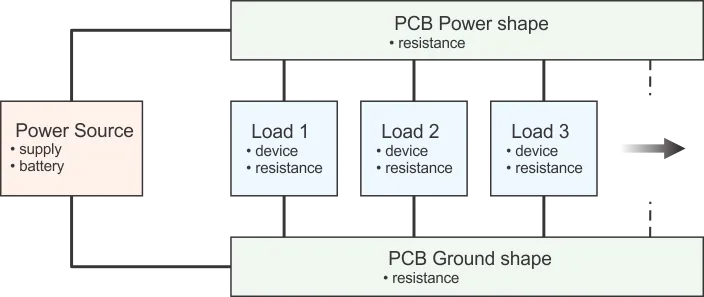
Figure 1: A basic block diagram of the power and ground shapes, and the applied loads.
Figure 1 (above) shows a simple block diagram of a circuit's power source and its power and ground shapes (traces and planes) that deliver power to the various loads (memory, microcontrollers, etc.). Note that all the loads are tied to the same power and ground shapes, and depend on those shapes to provide their operating voltage(s). In general, we tend to assume that those power and ground shapes have 0Ω resistance, which isn’t necessarily true, and that assumption can cause problems. Because relatively large currents are often involved, even small resistances in the power and ground shapes can cause significant power consumption (loss) and voltage drops.

Figure 2: 'IR Drop' effects
Figure 2 demonstrates an example of the problems that can arise if the resistance of the power and ground shapes are not properly considered. Even though each shape has a relatively small resistance of only 0.25Ω, they have caused the voltage at the load to drop from 5V to 4.5V. The designer has to be aware of this drop and ensure it can be accommodated, or change the design to lessen it, to ensure that that the final design will not fail in the field.
The problem, however, seems easy to solve – simply make the power and ground shapes short or large enough to represent an insignificant resistance, using the following relationship: R = ρ * L/A, where:
R is the total resistance of a shape (trace or plane)ρ is the resistivity of the material used for the shape (typically copper, ρ ≈ 1.7µΩ-cm)L is the length of the shapeA is the cross-section area of the shape (width x thickness)
Put simply, if you make your power and ground shapes short, thick and wide, you will minimize their resistance.
The difficulty with that, however, is that overly large shapes consume valuable routing space and may limit the amount of space for other voltage shapes. A design which has the properly sized power and ground shapes will be more compact and use fewer layers than one which arbitrarily uses overly large planes or traces. The intent of PI-DC analysis is to inform a designer that the board design's power and ground shapes are adequate, but not overly large.
Another consideration for IR drop is the fact that the amount of power consumed is I2R – so a small increase in current through a resistance causes a large increase in power consumption. This can manifest itself as thermal problems where the design heats up significantly because the power and/or ground shapes are not large enough to accommodate the current passing through them. By ensuring very small IR drop through power and ground shapes, power consumption in those shapes is minimized.
At the extreme, if a shape is resistive enough (very narrow and long) and has sufficient current flowing through it, that shape essentially becomes a 'fuse', thereby melting the copper shape and causing the design to fail – and possibly presenting a dangerous situation. The IPC-2152 standard for PCB current carrying capacity addresses this issue, but with pessimistic assumptions (no nearby thermally conductive copper to help draw heat away, for instance) and designers often apply that specification using the most conservative assumptions, such as only allowing a minimum temperature increase. While PI-DC cannot replace the IPC-2152 standard as a guideline for thermal considerations, it can give valuable insight into how a design can safely be optimized by studying the voltage drops and current densities of the power delivery system. A design that is optimized for the lowest current density and voltage drop between the sources and all loads will also generate less heat and have less chance of thermal issues.
Another aspect PI-DC analysis addresses is the number of vias used for power delivery. The problem is quite similar to that of sizing the copper shapes properly: if there are not enough vias, voltage is lost and power is wasted through IR drop, but if too many vias are used, valuable routing real estate is wasted. In particular, if too many vias are used for a particular voltage path, those vias pass through shapes on other layers and reduce their copper cross-section, thereby causing problems for those other voltages. In the same way as correctly dimensioning shapes, analyzing the voltage at the load points allows proper via sizing and/or numbering.
Finally, there is a significant advantage in simulating the final design exactly as it appears physically, to ensure it is optimized. PI-DC simulation provides a final check that connectors and regulators are sized appropriately, in case loads have been dropped or added during the design process, for example.
In the absence of reliable data on the voltage drop through a PCB's various power shapes, ground shapes and vias, a designer is forced to be conservative by using excessive plane shapes, trace sizes and vias, which consume valuable design real estate and increase layers and the design form factor. The Altium PDN Analyzer provides accurate information about a design’s DC power distribution suitability in an easy-to-use and straightforward manner to enable designers to make the most efficient power distribution designs possible.
Not only are the results suitable for final design verification, but they can also be used in the planning stages of a design to architect power delivery as efficiently as possible in advance. PI-DC is an invaluable tool in achieving the most efficient and robust power delivery network possible, the PDN Analyzer makes running that simulation and analysis process straightforward, intuitive and efficient.
Among these and other advantages that the PDN Analyzer brings to your PCB designs, it also delivers the following benefits:
- Product reliability: Helps to ensure the correct performance of individual supplies within the design, in terms of standing voltage levels, voltage stability, and trace heating/damage.
- Improved PCB layout: Provides information that can be applied in creating the most effective use of board space, and allows the easy identification and correction of problematic high current density areas.
- Knowledge: No longer rely on a rule of thumb approach or approximate calculations when considering the layout of DC current paths.
PDN Analyzer Simulation
In its most very basic form, a board layout that will be subject to PI-DC analysis might be composed of a Voltage Regulator source and its load, with interconnecting copper areas of various shapes and track widths.

A base circuit example of a power source and load.
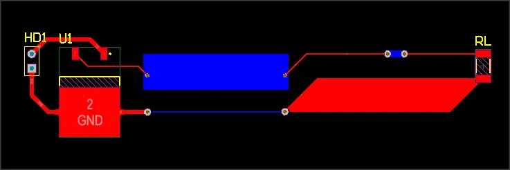
The base circuit's PCB layout, with a range of copper shapes and traces connected by layers and vias.
The PDN Analyzer panel interface (Tools » PDN Analyzer) visually emulates a Power Source to Load circuit net that incorporates tangible Power and Ground paths – much as shown in the above circuit and also the conceptual block diagram (Fig. 1). The application automatically extracts all physical and electrical information (netlist, devices and layer shapes, etc) from the currently active PCB design, which provides data for the PI-DC simulation engine.
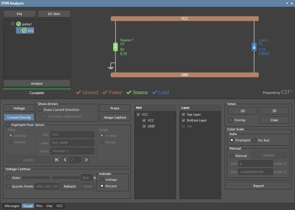
The PDN Analyzer panel interface showing a PI simulation setup for the basic circuit and board layout.
Here, the voltage source is the output of U1 (5V between pins 3 and 2), and the load is a specified current through RL (0.1A). Once the initial parameters have been entered via the interface (source/load voltages and currents, etc) and the simulation has been run, the resulting analysis data is graphically modeled in the PCB editor as a rendered 2D or 3D image.
 The Voltage Drop simulation results for the board's PWR and GND nets copper (U1 to RL, and RL to U1).
The PDN Analyzer PI simulation can be set to show Voltage (IR Drop, above image) or Current Density (below image) results for all applicable board layers.

The Current Density map for both the PWR and GND nets (U1 to RL).
See the collapsible section below for details on the user interface of the PDN Analyzer panel.
PDN Analyzer Panel
Layout Modes
The dockable PDN Analyzer panel is best used in conjunction with the software's PCB Editor so the visual results of analysis run may be seen immediately in the design's copper layout. In its floating (undocked) mode the panel might be moved to a second monitor to maintain visual access to the PCB Editor, or the panel may be vertically/horizontally docked in the main design screen to share real estate with the PCB Editor.
For the latter case, the panel offers a compact interface mode that moves its main configuration pane to a separate tab option (Config). To switch to this mode, select the Compact Layout option from the panel's  button drop down menu in the configuration pane/tab.
 In Compact Layout mode the Configuration pane changes to tab access, which preserves screen space for the PCB Editor.
Configuration
The Configuration pane (or Config tab) is devoted to simulation network control and presents an interactive graphic representation of the currently selected power network(s).
Simulation and network management
The section on the left of the Configuration pane/tab is used for simulation file management, and provides a hierarchical view of the simulation's loaded power networks. The complete network structure or individual power networks may be selected. The section's options include:
- The
 drop down menu.
- New Simulation – start a new PDN simulation, based on a single power/ground network.
- Open – open a previously saved or example simulation configuration file (
*.pdna).
- Save – save the active simulation configuration to disk as the current name.
- Save As – save the active simulation configuration to disk as the desired name.
- Explore – open a Windows file browser in the location of the active simulation.
- Explore Samples – open a Windows file browser in the location of the installation's example project (stored as a zip archive) – unzip this project to a convenient location. Note that the project also includes a set of example PDN Analyzer configuration files, where each is set to a specific copper temperature; 25°C (nominal), 100°C, 175°C.
- Compact layout – the alternative screen mode outlined above.
- Right click options – accessed by right clicking on the top level simulation name.
- Import (1.x) – load a simulation configuration saved from the previous
1.xx version of the PDN Analyzer (*.pidc_config).
- New Network – create a new base-level network within current simulation configuration.
- Remove – unload the selected simulation.
- Delete – remove the selected network from the simulation (available as a right click option on the name of an individual network).
- Clear Results – reset the power network analysis results, including those cached from a previous simulation run.
- Revert – restore the last simulation analysis results and its corresponding configuration.
- Save – save the active simulation configuration to disk as the current name (
*.pdna).
- Save As – save the active simulation configuration to disk as the desired name.
- Copy – clone the selected network simulation.
- Explore – open the
/PDNAnalyzer_Output folder for the current simulation in a Windows file browser. Note that this includes a fully detailed event log file for the most recently run simulation (PDNAnalyzer.log).
- Settings – opens the Settings dialog for the current simulation configuration. The settings can be exported/imported (
*.pdna.settings) and reset to their defaults.
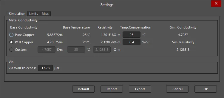
The dialog includes the:
- Simulation tab – specify the Metal Conductivity settings for the physical board copper and the weight (wall thickness) of the layer connection Vias.
- Limits tab – specify the maximum current density limits detected by the simulation for both copper layers and Vias of two sizes.
- Misc tab – set simulation parameters such as the applied current density units and data smoothing (Noise Filtering), and voltage offset scheme used to establish the design's zero voltage reference.
- The
 button, which opens the PDN Analyzer DC Net Identification dialog – also opened when the PDN Analyzer is first invoked. The system will attempt to automatically detect suitable DC power nets within the current PCB design.
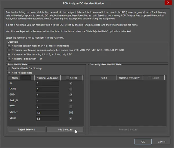
Use the dialog options to help correctly identify the DC nets and their nominal voltage levels.
- Qualifiers – deselect qualifier filters if necessary to correctly identify the design's DC nets. The filters are based on number of connection and common power network nomenclature.
- Potential DC Nets – a tabular list of the identified power net in the design. Use the Enable all and/or Hide rejected options to populate the list as needed for your DC power analysis.
- Name – the net name as extracted from the board design's net data. Use the associated search field to filter the listing by an entered key word.
- Nominal Voltage – enter a suitable voltage for power nets as basic source data for the analysis.
- Select – use the checkboxes to nominate which nets would like to be registered (identified) by the PDN simulation.
- Reject/Add Selected – use the
 and
and  buttons to manage which nets are populated into the Currently Identified DC Nets listing.
- Currently Identified DC Nets – a tabular list of power nets that will be available to the PDN simulation, as populated from the Potential DC Nets listing.
- Select – use the checkboxes to select nets that will be removed (moved from the identified nets list back to the potential nets list) by the
 button.
Click on a net entry to cross probe to that net in the PCB Editor.
- The
 button, which invokes the power network simulation and analysis routines. This button is enabled when the power network and its related data is fully configured, as indicated by tick icons associated with the Ground, Power, Source and Load labels in the power network diagram graphic.
Power Network Graphic
The main body of the Configuration pane provides an interactive graphic representation of the power network structure selected in the simulation's network tree (on the left). When the top level simulation name is selected, the graphic shows the overall connectivity of sub power networks – double click on a sub network graphic element to open that sub network. The interactive graphic also is used to construct a power network from the PCB design's net data and connectivity by using its right-click options, or by double-clicking on graphic elements.
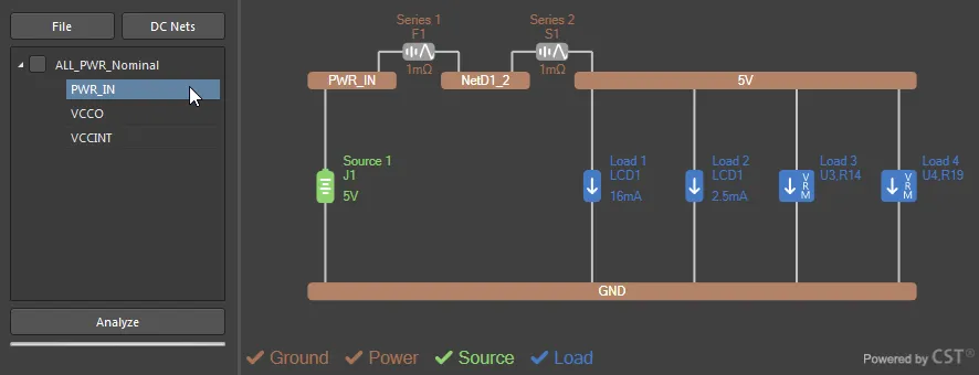
Hover the cursor over an active element (Source, Load, series device, etc) to see a summary of its properties, connectivity and if applicable, analysis results.
► See Example 1, Example 2 and Example 3 in the PDN Analyzer Example Guide for detailed information on creating various types of power networks.
Right click on the configuration graphic or one of its elements to access the following options:
- New Network – create a new base-level network (power and ground nets) within current simulation.
- Edit Net – specify a power network's settings in the Choose Net dialog (also available by double-clicking on a network element). The dialog includes a selectable list of nets available to the simulation (as defined in the PDN Analyzer Net Identification dialog, opened from the
 button) and several filter options that can be used to constrain the listing.

- Extend Net – use to add another net to the selected net via a series element, which will be inserted automatically. The additional net is selected in the Choose Net dialog, while the inserted series device is configured by double clicking on its element to access the Device Properties dialog. See Extending Networks Through Series Elements for more information.
- Add Source – add a Voltage or Voltage Regulator Model (VRM) source device between a specified power/ground net pair via the Device Properties dialog. The dialog also is available by double-clicking on an existing Source element. See Including Voltage Regulator Models for more information on working with VRMs.
- Add Load – add a Resistor, current sink or Voltage Regulator Model (VRM) load device between a specified power/ground net pair via the Device Properties dialog. The dialog also is available by double-clicking on an existing Load element.
- Delete – remove the power net from the simulation. Note that a network must include one power net and one ground net as a minimum.
- Settings – open the Settings dialog, as outlined above.
The Device Properties dialog, used when adding or editing an existing device element (Load, Source, etc) provides settings to specify the device type, connectivity and parameters.
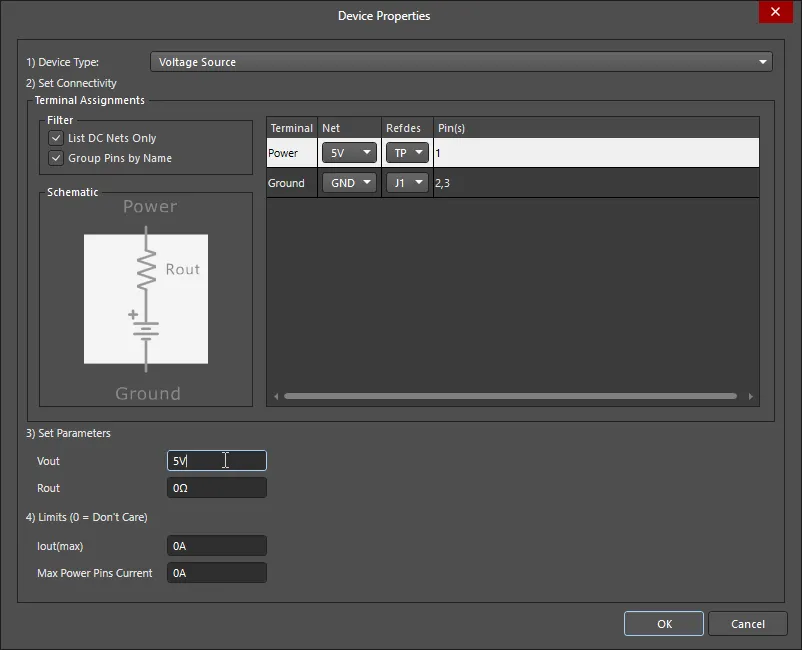
The dialogs's available settings options will depend on the function of the device element being placed or edited, but are generally as follows:
- Device Type – use the drop down menu to select type of device, where the available options are determined by the element type (Source, Load, etc).
- Set Connectivity – use the listing's Net and Refdes dropdown options to choose the device's Terminal connections from the available nets and nodes, where the Terminals are as indicated in the Schematic simulation model graphic. The net connection Pins are automatically assigned based on the specified node's net connectivity.
- Filter – use List DC Nets Only option to constrain the available Net options, and the Group Pins by Name option to combine interconnected device pins. When the latter is disabled, individual pins can be selected/deselected as required using the Select checkboxes exposed by clicking in the Pins field. See the LCD example in Working with Loads for more information.
- Set Parameters – the available parameter options will depend on the type of device being placed (or edited), but generally define its base properties such as the output voltage and internal resistance of a Voltage Source, the load current of a Current sink, or the resistance value of a Resistor load.
- Limits – the device's Voltage, Current or Power limitations that will trigger a Violation when the simulation is run. A violation is indicated by a dashed red border around the graphic of the offending element and a red icon associated with the network name: see Current Density Limit Violations or Other Violations for examples.
Messages tab
The Messages tab includes a sequential listing of simulation events for the most recently run PDN analysis, including any Violations that were encountered. In the situation of a failed simulation run, the list will include an event entry summarizing the issue. For more information on a simulation run, see the PDN_Analyser.log file available via the configuration Explore option.
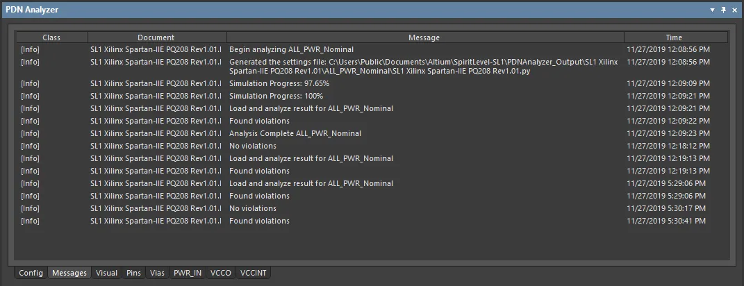
Visual tab
The PDN Analyzer interface's Visual tab provides a high level of control over how the power network analysis data is displayed in the PCB Editor. It allows you to specify what type of information is included in PCB layout rendering, the scaling of the results data, how and if points of interest are highlighted, and what information is exported. The rendered layout in the PCB Editor applies to the power network that is currently selected in the PDN Analyzer's Configuration network hierarchy.
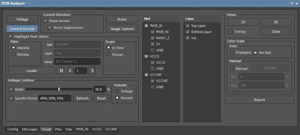
Use the Visual tab's default settings as a starting point for setting up the PCB layout display. These are set to show the color-graduated voltage profile across all power rail nets in 2D mode – deselect the Overlay option to see the pure analysis results. Setting changes made in the Visual tab are immediately reflected in the PCB rendering.
The Visual tab options include:
- Voltage – select the
 button to display the voltage profile across all enabled nets, scaled in Volts or as an overall percentage span (see Color Scale).
- Current Density – select the
 button to display the current density profile across all enabled nets, scaled in Amps per area or as an overall percentage span (see Color Scale).
- Current Direction – check the Show Arrows option to overlay current direction/distribution indicator arrows on the rendered PCB layout. Select the Noise Suppression option to apply data smoothing for a less cluttered visual result.
- Probe – select the
 button to open the Probe dialog, where two data locations in the rendered layout can be interactively selected and their numerical values compared. See Data Probe for more information.
- Image Capture – select the
 button to open the Manage Image Capture dialog, where the current PCB rendering can be captured and saved. The images are stored in the project simulation's
 /HTMLReport/ImagesCache folder for later inclusion in a Report. See Analysis Report for more information.
- Peak Values – select the Highlight Peak Values option to visually mark and highlight the maximum or minimum (as per the Filter options) Value in the currently selected nets and layers. Use the Scope options to specify the detection area, the Locate button visually highlight the peak value point, and the data point arrows (

 ) to step though the adjoining sequence of values. See Locating Power Integrity issues for example information.
- Voltage Contour – select the Slider option to enable a dashed line overlay which represents the voltage level at that contour line. The detected level is that set by the slider position, and is a voltage or percent value as determined by the associated Indicate options. Select the Specific Points option to enable voltage contour lines at each on the indicated percentage points. Click
 to set the Specific Point values to their defaults, and the
  button to update/highlight all enabled voltage contour lines. See Voltage Contour for more information.
- Net – select the Nets you wish to display in the rendered PCB analysis results. The nets are grouped by available power networks.
- Layer – select the board Layers you wish to display in the rendered PCB analysis results. Note that Vias are available for selection when in 3D view mode.
- Views – use the
 and
and  buttons to change the rendered display between the PCB Editor's 2D/3D modes, the Overlay option to enable/disable the editor's standard PCB display view, and the
  button to revert the rendered display to the standard view. See Display Control and Options for more information.
- Color Scale – set the Auto options to show the rendered color gradient as an overall percentage range (Per Rail) or as a gradient that corresponds to the complete voltage span data (Displayed). The latter is best used when a single net is being displayed. Select the Manual mode to override the displayed range to the voltage values entered in the Min and Max fields. See Visual Rendering in the PCB Editor for more information.
- Report – click the
 button to configure and generate an HTML-based PDN Analysis report via the HTML Report dialog. See Analysis Report for more information.
Pins tab
The Pins tab presents a list of all component pins in the design connected to configured power networks. Each component pin entry includes its number, connected net, and the associated Voltage and Current value results from the last simulation run. Click on a column header to order the list by that name, and click again to reverse the order.
Double click on an entry to cross probe to that pin in the PCB Editor. If the pin (pad) connection cannot be seen in the rendered view, ensure that the Layer and power Net it is connected to are enabled in the Configuration pane/tab.
 The Pins tab listing ordered by Component reference and – hover the cursor over the image – ordered by pin Current.
Vias tab
The Vias tab presents a list of all PCB vias in the design connected to configured power networks. Each via entry includes its connected net, location co-ordinates, layer pair, and the associated end-to-end Voltage, Current and Current Density value results from the last simulation run. Click on a column header to order the list by that name, and click again to reverse the order.
Double click on an entry to cross probe to that via in the PCB Editor. If the via cannot be seen in the rendered view, ensure that Via is checked in the Layer list (available in 3D view) and its connected power Net is enabled in the Configuration pane/tab.
 The Vias tab listing ordered by Net connection and – hover the cursor over the image – ordered by Current Density.
Power Network tabs
A tab view is available for each available power network within the simulation configuration – the network tabs that are visible is determined by the power network selection in the Configuration pane/tab. Labeled as the network name, the power network tab provides a comprehensive listing of grouped simulation results and calculated data that applies to that power network. A network power consumption summary is also included.
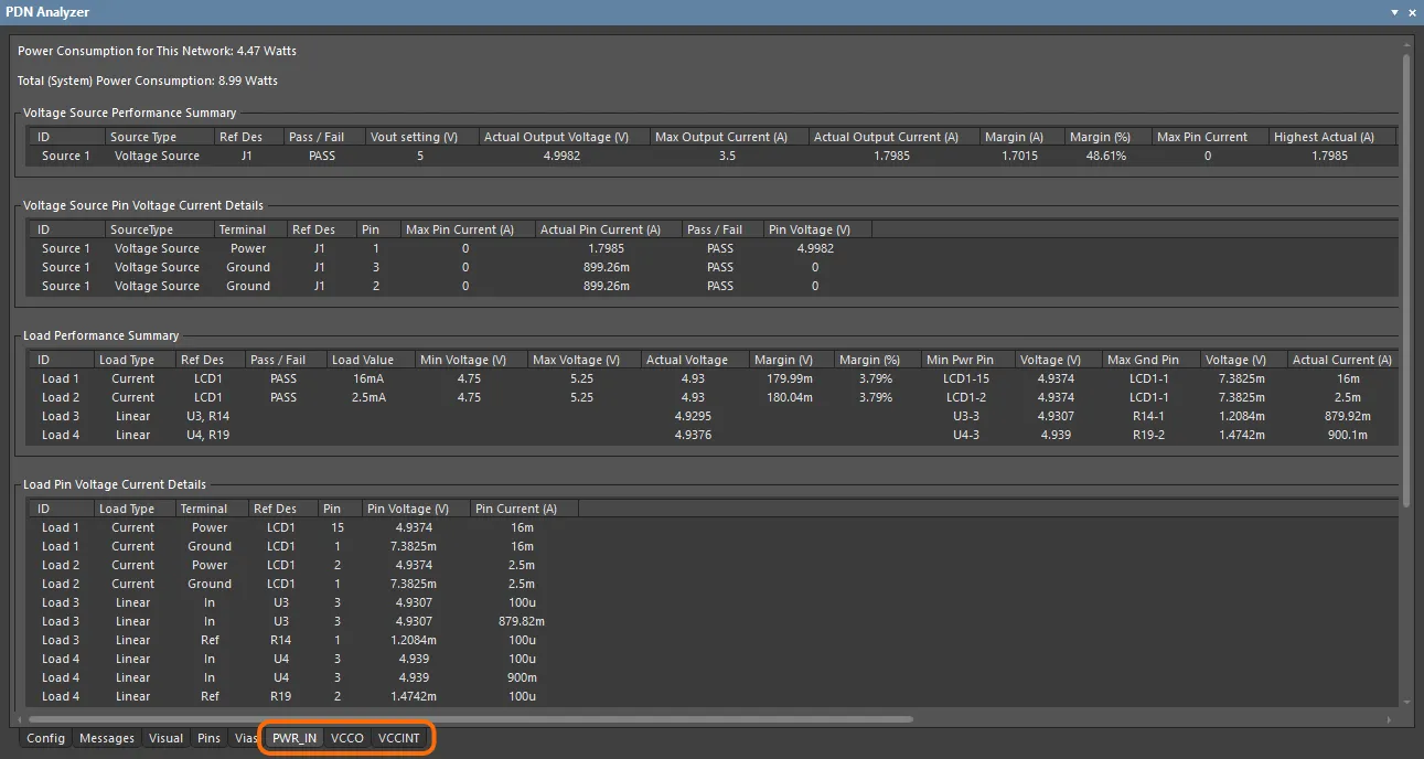
The data groups in the listing apply to devices within the power network (sources, loads, and series elements), where a Performance Summary and a Pin Voltage/Current Details data entry is included for each device. Along with details about the device, the data groups present key voltage and current values, and in the case of the Performance summary, calculated safety margins that relate to the device limits as specified in the Device Properties dialog.
► See the PDN Analyzer example guide for a complete description of using the PDN Analyzer and interpreting its results.
The PDN Analyzer installation includes Altium's SpiritLevel-SL1 PCB reference project with a number of PDN analysis configuration file examples. Access and then unzip the project and samples from the PDNA File » Explore Samples menu option.
Installation and Licensing
The PDN Analyzer application is added to Altium Designer by installing the PDN Analyzer Extension. Its functionality is enabled with a matching software License.
Installation
The PDN Analyzer is installed (and updated) from the software's Extensions & Updates view, which is accessed from the User drop-down menu ( ) located at the top right of the Altium Designer GUI.

Select the Purchased tab in the Extensions & Updates view, locate the PDN Analyzer icon and then click its  button to download and install the extension. Restart Altium Designer to enable the application.

The extension icon, prior to the PDN Analyzer's installation.
A timed Trial License may be offered for the PDN Analyzer. If you wish to use the PDNA on an evaluation basis, follow through the guided steps and confirm the license activation in the
License Management view. Otherwise, proceed with a standard license scheme as
described below.
Once installed, the extension will appear under the Extension & Updates view’s Installed tab. The PDN Analyzer tool is available from the Altium Designer Tools menu as PDN Analyzer when a Schematic or PCB project document is open. Note that if the PDN Analyzer is unlicensed, a related error message will appear – see below for license activation steps.
Once installed and licensed, the PDN Analyzer icon will also appear under the Updates tab (in Extensions & Updates) when a new version is available for download. Hover the mouse cursor over the icon's download button to see the version information, or select the extension's title to expose more information.
► See the Altium Designer Extensions page for more detailed information about installing and managing extensions.
Licensing
The PDN Analyzer can be licensed using any of Altium's standard License schemes; by activating an On-demand or Standalone license from Altium's License Server, or from an internal network Private License Server.
► See the Altium Designer Licensing page for more information on Altium licensing and types of licenses.