Our 3D-MID tool brings true 3D circuit design to Altium Designer for the first time, allowing you to combine electrical and mechanical functionality into a single part.
A 3D-MID document integrates into your Altium Designer project in the same way as a standard PCB - its components and connectivity are driven by your schematic design, and it incorporates standard SMT footprints from your usual component library.
What is 3D-MID?
3D-MID stands for Three-Dimensional Mechatronic Integrated Devices.
The 3D-MID manufacturing process uses a laser to etch the circuit pattern directly onto the surface of a 3D substrate, which then undergoes a standard metalization treatment to build up that pattern into conductive pathways. This process, known as Laser Direct Structuring (LDS), enables the circuit to be integrated into the structure of the final product.
Designing circuit pathways over the surface of a 3D structure brings unique challenges. The editing space must support the placement of components and the connections between them that define the unique circuit. This editor must also be able to import the 3D substrate on which the electronic circuit will be created - it must be a true, three-dimensional electronic design editor.
The designer must be able to position the components onto any surface of the imported 3D substrate. They must then be able to define the connective pathways between the component pins, a process commonly called routing the connections. Again, those routes must be able to travel over the surface of the substrate, regardless of the current orientation of the substrate surface at any point along the route path.
Finally, the designer must be able to generate the manufacturing data in the format required by the Laser Direct Structuring (LDS) process.
The new 3D-MID design tool brings this functionality for the first time to Altium Designer.
Notes
-
Graphics requirements:
-
Minimum: Graphics card (supporting DirectX 11 or better) such as GeForce 400 series/Radeon HD 5000 series/Intel HD 4600
-
Recommended: High-performance graphics card (supporting DirectX 11 or better), such as GeForce GTX 1060/Radeon RX 470
-
The 3D-MID functionality is in Open Beta and available when the System.3DMID option is enabled in the Advanced Settings dialog.
-
If you're new to PCB design and Altium Designer, you might like to complete the introductory tutorial for 2D PCB design. It will take you from a blank schematic page to a completed PCB, explaining how to create a project, find the components, capture the schematic, define the connectivity, define the routing widths, and much more - A Complete Design Walkthrough with Altium Designer.
-
You can share your questions, thoughts and ideas about how to improve the 3D-MID tool by posting in the Altium Designer forum or contact the development team directly by emailing 3d-layout@altium.com.
Creating a 3D-MID Document
In the same way as a standard PCB document (PcbDoc), a 3D-MID document (PcbDoc3D) can be either created within a project or as a free document.
-
To create a new 3D-MID document from within a project, right-click on the project name in the Projects panel, then select Add New to Project » PCB3D.

-
To create a 3D-MID document as a free document, select File » New » PCB3D from the menus.

-
As part of the creation process, a dialog box will appear, prompting you to select a file to form the substrate of the 3D-MID document. The file selected must either be in STEP or IGES format. The advantage of the IGES format is that it can include embedded sketches.
Note: only single-part (not assembly) STEP or IGES files are fully supported. If an assembly file is selected, only the first part of that assembly will be imported.
Once selected, the substrate file will be displayed in the 3D-MID editing window. If you cancel the substrate selection window, the default substrate will be displayed, as shown below.
 A default 3D substrate is created if you choose not to open your own.
The name of (and full path to) the 3D substrate file is presented in the Properties panel. When no object is selected in the 3D-MID document, open the panel's Parameters tab and locate the Pcb 3d Substrate File Name parameter – show example. The parameter value will be updated if you change the 3D substrate using the File » Change Substrate command, as described below. Note that it will not be updated if the 3D substrate file is renamed (e.g., through the Windows File Explorer).
Changing the Substrate
If required, the 3D substrate can be changed by selecting the File » Change Substrate command from the main menus.
 If the substrate design has changed, it can be updated.
How Existing Objects are Handled when the Substrate is Changed
|
|
When a new substrate is selected, the software compares the new substrate against the existing substrate.
It does this by comparing the location of each existing surface against that surface's location in the new substrate.
Using a threshold, if the new surface is within the distance specified to an existing surface, it is considered the same surface in a new location, and any existing layout objects are moved onto it. Greater than this distance, the new surface is considered a different surface, and the layout objects are deleted.
The threshold value is defined by the Advanced Option 3DLayout.ChangingSubstrate.MaxDistance, which has a .001 mil resolution with a default value of 2000 (2 mils).
|
Working in the 3D-MID Document Editor
The camera controls are as follows:
-
To pan, drag with the right mouse button
-
To zoom, use the scroll wheel
-
To rotate, hold shift and drag with the right mouse button. The center of rotation is defined by the location of the mouse pointer when the command is initiated.
-
To center your view of the substrate in the middle of the screen, press the Ctrl+PgDn shortcut (View » Fit Substrate).
-
By default, 3D bodies contained in any of the component footprints in the design will be visible. Depending on the footprints and the layout, it may be easier to hide these temporarily during layout work. This can be done using the View » Component Bodies » Hide and View » Component Bodies » Show commands (shortcuts: 2 to hide, 3 to show).
Changing Your View of the Substrate
On the bottom left of the design space is a red/green/blue axis marker, referred to as the view orientation Gizmo.
 Click on a colored plane or axis in the Gizmo to reorient your view of the substrate to that plane/axis.
The Gizmo
The Gizmo is used to change the orientation of your view of the substrate. Each workspace axis and its corresponding plane is assigned a color. As you hover the mouse over a colored Gizmo element, it will become larger, indicating that it is active. When you click on that colored element, the view will reorient, so you are looking down that axis into the substrate. A second click will flip the view over, looking along the same axis from the other direction.
-
Blue - Z axis, viewing into the X-Y plane.
-
Red - X axis, viewing into the Y-Z plane.
-
Green - Y axis, viewing into the X-Z plane.
3D View Controls
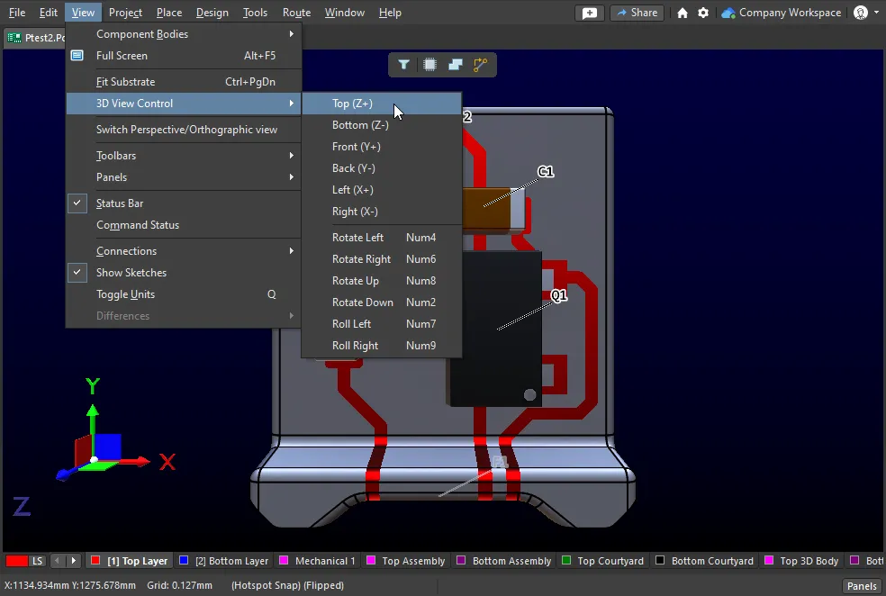
Your view of the substrate can also be controlled via the 3D View Control sub-menu.
-
Use the upper set of commands to view the substrate along the specified axis.
-
Use the lower set of commands to Rotate or Roll the substrate in the chosen direction. Each of these commands can also be accessed by the shortcut detailed in the image below. Selecting a Rotate or Roll command will also perform a zoom to center the substrate in the middle of the screen.
Changing the View Type
You can change the view by toggling the View » Switch Perspective/Orthographic view command. The Perspective view lets you see a more realistic 3D view of the 3D-MID. The Orthographic view removes the distortion effects due to perspective and ensures parallel features are displayed as such.
Configuring the Colors
The substrate surface color and outline color, as well as the color of the currently selected object and the copper, can be configured in the View Configuration panel, as shown below. Enable the panel via the Panels button at the bottom right of the software.
|
|
The substrate surface color, outline color, and the color of the currently selected object can be configured in the System Colors section of the panel.
The color of the copper can be configured in the Layers section of the panel. The graphics window will not show the new copper color until the components’ visibility has been toggled using the 2 and 3 shortcuts.
|
Alignment Tools
There are two tools available to help locate entities on the surface of the substrate. You can import a sketch from MCAD or use the Alignment Grid generation feature in the 3D-MID editor. Once displayed, the sketch entities can be used to aid the placement of components, copper traces and regions.
-
When dragging a component, the mouse pointer will snap to the center of the footprint. The mouse pointer (and therefore the component center) will then snap to the sketch elements.
-
When a component is selected, it will also display a rotation handle. Click and drag the handle to rotate the component. The handle will snap to the sketch elements. Learn more about interactive component rotation.
-
When routing, the copper trace start, and endpoints will snap to any intersections formed by sketch elements. If the mouse pointer is not near any intersections, it will snap to the sketch lines. If during routing, the mouse pointer is moved along a sketch line (including curved lines), the trace will follow that line.
-
The vertices and edges of a region can also be aligned to the grid or imported sketches.
-
The two tools described below can be used independently at the same time on the same substrate.
Sketch Import
-
When designing the substrate in MCAD, 3D curves can be placed on the surface of the part and included in the exported IGES file.
-
In Solidworks, for example, the Project Curve command allows you to place a 2D sketch onto a 3D surface.

-
These “curves” can then be included in the IGES export using the Export 3D Curve features option.

-
When the IGES file is imported into Altium Designer to form the substrate for a 3D-MID, these elements can be displayed by selecting the View » Show Sketches command.
 Sketches defined in MCAD are shown in red.
-
The sketch features can then be used as a guide for placing components and regions, and during routing.
Alignment Grid
-
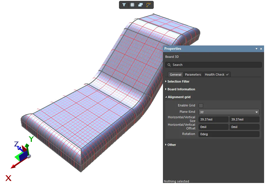
From within the 3D-MID document, it is possible to generate a grid on one of the three datum planes using the Alignment Grid section of the Properties panel when there are no objects selected in the 3D design space. This grid is then projected from the specified plane onto the surfaces of the part. Note that this grid is independent of sketches imported as part of the substrate.
-
The properties of the grid can be controlled by the user. Note that the substrate origin is inherited from the imported STEP/IGES model.
-
Enable Grid - grid snapping only occurs when the grid is visible.
-
Plane Kind - the XY, XZ, YZ plane from which the alignment grid is projected. Inherited from the STEP/IGES model imported to form the substrate.
Alternatively, you can select UV plane kind that generates a grid based on the surfaces of the substrate, providing more natural gridlines that follow the curves of the substrate (show image). The UV plane kind allows routing along more 'natural' lines on the surface of the 3D substrate.
-
Horizontal/Vertical Size - pitch of the grid.
-
Horizontal/Vertical Offset - grid offset, relative to the substrate origin.
-
Rotation - rotation angle of the grid, parallel to that plane (applicable to XY, XZ, YZ plane kinds only).
Cursor Snapping
The 3D-MID document editor allows you to override snapping priority. The snapping priority controls are accessed using the Objects for snapping button ( ) on the Active Bar.

There are two levels of cursor-snapping available: grids and objects. When enabled, object snapping overrides grid snapping. This, for example, makes it possible to snap to the grid rather than to that trace's centerline when routing to/from an existing trace by enabling snapping to Grids but disabling snapping to Track Lines (provided the grid itself is enabled in the Properties panel), as shown in the video below.
Working with Components
-
If the 3D-MID document is part of a project, components can be synchronized to it from schematic sheets using the standard commands - Design » Update PCB if you are working in the schematic editor, Design » Import Changes from xxx.PrjPcb if you are working in the 3D-MID document editor. In this case, the schematic pin net assignments will also be transferred to the 3D-MID component pads. Note that there are default design rules created as part of this process, refer to the Default Project Options and Design Rules section of this page to learn more.
-
Once synchronized to the 3D-MID document, the components will initially appear floating in 3D space next to the substrate body and can be dragged one by one onto the surface of the substrate. The default behavior is that when you drag a component onto the substrate, the initial orientation of the component on the substrate surface will depend on the route taken with the mouse when dragging.
|
|
After synchronizing the components and nets from the schematic, the components appear next to the substrate floating on its X-Y plane. Note that pad 1 has rounded corners.
The orientation of the moved component after approaching the substrate from the front.
The orientation of the moved component after approaching the substrate from the side.
|
-
Alternatively, components can be dragged straight onto the substrate from the Components panel. When you place a component from the Components panel, it has a default designator, and all of the component pads are designated as
No Net.
-
As you drag a component, the mouse cursor (indicated by a green cross) will snap to the centerpoint of the footprint. The cursor (and attached footprint centerpoint) will then snap to a visible alignment grid. Learn more about Alignment Grids and the Alignment Tools.
-
Components can also be dragged with the 3D bodies hidden. To choose the component, click and hold on one of the component's pads. As soon as the mouse is moved, the component centerpoint will snap to the cursor.
-
When dragging a component in a 3D-MID document and component bodies are hidden (View » Component Bodies » Hide; shortcut: 2), draft graphics (green pyramids) will be shown if its pin count is more than the limit defined by the 3DLayout.ComponentDrag.DrawShapesPinsLimit advanced setting (15 by default). This behavior is implemented to improve performance. The value of the setting can be adjusted to suit your PC's specifications.

-
When a component is being dragged, the Spacebar rotates it in increments defined by the Rotation Step angle defined in the PCB Editor - General page of the Preferences dialog (show image
![]() ). The default rotation step is 90 degrees.
). The default rotation step is 90 degrees.
-
The behavior of a component’s orientation, when dragged over different surfaces of the substrate, is controlled by
3DLayout.ComponentDrag.KeepOrientation advanced setting.
|
|
If the value is True (the default value), the algorithm will attempt to maintain the same component orientation as it passes over each surface boundary. The result of this is that a component’s orientation on any surface is dependent on the route it took to get to that surface.
If the value of the 3DLayout.ComponentDrag.KeepOrientation advanced setting is False, the algorithm will ensure that all components on the same surface have the same orientation, regardless of the route they took to get to that surface. This means that the user may expect to see a sudden change in component orientation as it is dragged across a surface boundary.
|
-
The orientation of a component can be defined using the rotation handle. To do this:
|
|
Click once to select the component. A box will appear around the component, and the handle will become visible. It can be used to interactively set the orientation of the component.
Click and hold this handle, and drag it to the desired position. The handle will snap to the alignment grid.
|
-
You can also drag more than one component. Select multiple components (using the Shift+Click shortcut or other selection methods), then use Click, Hold&Drag on the selection to move all selected components at once. As with dragging a single component, the movement is constrained by the current snapping options.
-
Pads, fills and solid regions within a component footprint are copper objects supported for placement in the 3D-MID document. This enables you to place components with complex-shaped footprints onto your substrates, including RF shapes (e.g., antennas).
-
When a component is dragged over the surface of the substrate, the shape of its pads is created by wrapping its shape from the plane of the 2D footprint onto the substrate surface. If this surface is not planar, the resulting shape of the pads will be distorted. There are limits to the level of distortion that can be tolerated. Once this limit is reached, the pad will not be created.
-
To access the properties of a component, left-click the component body. A wireframe box will appear around the component. Its properties can then be accessed via the Properties panel.
-
Once a component has been selected, a pad can be selected by a further left-click directly on the pad. The pad’s properties can then be edited via the Properties panel.
-
If the pad's properties are not available for editing, it means the global Protect Locked Primitives in Component option is enabled in the PCB Editor - General page of the Preferences dialog (show image). To override this locally and edit the pad of this component, select the component rather than the pad (the wireframe box will appear), then click the Primitives lock button (show image) to unlock that component's primitives. Remember to re-lock the component primitives when you have finished editing the pad properties.
Note that due to the lighting/shading effects in the graphics window, when a pad is selected, it can take on the same color as the substrate and may seem to disappear. If this happens, try rotating the camera to view the 3D-MID from a different angle or change the substrate or selected item color.
Routing
Routing is the process of defining copper pathways between the connected component pins. You route the design by replacing each net connection line with track objects on a copper layer.
Displaying the Connection Lines
As an aid to routing, it is possible to display the net connection lines (View » Connections » Show All). Connection lines are displayed between unconnected tracks/pads of the same net, reflecting the connectivity defined in the project schematic documents. For each net, the default approach is for the algorithm to calculate the configuration of lines, which minimizes their total length.
The component pads must be on the substrate for the connection lines to be visible.
Color-Coding the Connection Lines
-
The set of connection lines that make up each net can be color-coded, as shown below:
|
|
To apply a color to a specific net, first...
select a pad belonging to that net (click once to select the component, pause briefly, then click a second time to select the pad),
then click the Net hyperlink in the Properties panel.
Click the color icon, and choose a new color for that net's connection lines in the palette that appears.
Alternatively, using the PCB panel set to Nets mode, locate the net in the list and right-click on the name to display the context menu.
Select the Change Net Color command to open the Choose Color dialog, and select a new color.
|
Net Color Override – Displaying the Net Color on Routed Nets
You can also use the net color for routed nets by enabling the Net Override Color feature. This feature affords you control over the highlighting of routed nets on your 3D-MID documents using your own overriding color scheme. Instead of purely having a net object colored using the layer color, you can assign to use a specific alternative color.
To use the Net Override Color feature:
-
Apply the required color to the net(s) – use the techniques described in the Color-Coding the Connection Lines section above.
-
Enable Color Override for the net(s) – color override is enabled for each net using the checkbox next to its name in the PCB panel (in Nets mode), as shown for the net
NetR2_1 in the image below. The checkboxes can be toggled for multiple selected nets via the Right-click » Display Override » Selected On/Off commands.

Preparing for Routing
-
Once a connection is routed between two pads of the same net, the associated connection line disappears. This allows the connection lines to be used as a visual check to ensure all nets are fully routed - for a fully routed design, no connection lines will remain (other than between a pair of via pads). If required, the connection lines can be hidden using the command View » Connections » Hide All.
-
Only manual interactive routing is supported (automatic routing is currently not supported).
-
There are two interactive routing modes available:
-
Ignore Obstacles - connection to copper of a different net must be avoided manually. It is possible to create short circuits. In this mode, the software will be fast and responsive.
-
Walkaround Obstacles - the routing algorithm prevents short circuits by maintaining a clearance between the route and copper objects in a different net. This is a calculation-intensive process, so there may be a lag before the software detects the collision and wraps the route around the obstacle. The algorithm requires the cursor to be outside the object belonging to the different net.
Select the Tools » Preferences command to open the Preferences dialog, then open the PCB Editor - Interactive Routing page of the dialog to select the routing mode. Although it is possible to select other routing modes, these are for 2D PCB design. If one is selected, the software will default to Walkaround mode.
Setting the Object Clearance and Routing Width
The 3D-MID editor uses Design Rules to define the width of the routing and the minimum clearance allowed between objects that belong to different nets.
-
To set the clearance and routing width requirements, open the PCB Rules and Constraints Editor (Design » Rules).

Configuring the Clearance Constraint
-
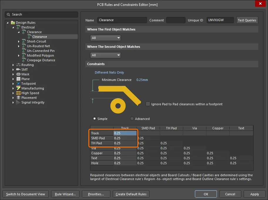
In the tree on the left of the design rules dialog, expand the tree and select the default Clearance rule.
-
Only the three values highlighted in the image below affect the algorithm:
-
Note that TH (thruhole) pads are recognized in the 3D-MID document as such, but the hole itself will not be included.
Configuring the Routing Width
-
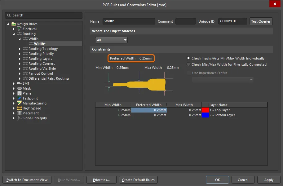
The width for newly placed tracks is defined by the applicable routing Width design rule. The 3D router only supports the Preferred Width value for the Top Layer. This can be configured in the overall Preferred Width field (highlighted in the image below) or in the layer-specific width field.
Default Project Options and Design Rules
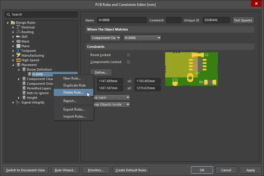
Every new project has default rule-creation settings, and every new PcbDoc3D document has default rules. For example, the default project settings will result in the creation of one or more Placement design rules when the design is synchronized between the schematic editor to the PCB3D editor. The consequence of this default Placement rule is that the online DRC will detect that the components are not contained within the room, so they will be highlighted (in green) as being in violation.
-
The default Placement design rule can be deleted; right-click on the rule in the PCB Rules and Constraints Editor to display the context menu and delete it, as shown below. Learn more about Design Rules.
-
To prevent the software from creating a Placement rule for each schematic sheet in the project when you synchronize a design between the schematic and 3DPCB editors, open the Options for PCB Project dialog (Project » Project Options), switch to the Class Generation tab, and disable the Generate Rooms option, as shown below. Learn more about the Project Options.

Routing with the Alignment Grid and Sketches
Because you are routing connections across the irregular surfaces of 3D objects, the traditional XY-plane grid used in PCB design does not make sense. Instead, the 3D-MID editor supports two types of sketch features: the Alignment Grid and imported Sketches.
-
The 3D-MID editor Alignment Grid is enabled and configured in the Properties panel when there are no objects selected in the design space. Configure the Alignment Grid properties to suit the required routing pitch, including the:
-
Plane Kind (the plane from which the Alignment grid is projected);
-
Size (pitch of the grid) and
-
Rotation (rotation angle parallel to that plane). During routing, as the mouse pointer approaches the alignment grid, it will snap to the nearest grid line.
-
If the substrate is imported from an IGES file, any sketch features (lines and arcs) embedded within that IGES file can also be used as a guide for the placement of routes. During routing, if the mouse pointer is moved towards a sketch line intersection, it will snap to that intersection. Otherwise, it will snap to a nearby sketch line. Note that the sketches can only be used for placement if they are visible. To toggle their visibility, select the View » Show Sketches (note that this command does not apply to the display of the Alignment Grid; this is configured in the Properties panel).
 Enable the Alignment Grid to snap routes to the grid.
Routing a Connection
To start routing, select the Route » Interactive Routing menu command, click the shortcut button in the Active Bar as shown below, or press the Ctrl+W shortcut combination.

Routing is the process of defining copper pathways between the connected component pins.
Tips for routing
-
Launch the Interactive Routing command. The cursor will change to a green cross to indicate that the interactive routing command is active. Note that there may be a brief delay between selecting the command and being able to start routing the first time you launch the command in an editing session.
-
Click anywhere on the pad (or existing route) of interest to start routing. A track segment will appear, the fixed end will automatically attach to the pad center (or existing track end), and the other end will be attached to the moving cursor. The track segments you place with each mouse click will automatically be assigned the Net of that pad or existing route.
-
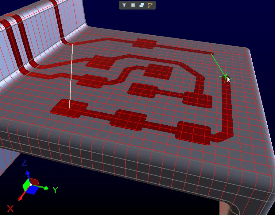
The moving end of the route will have a green interactive connection line attached to it. The software will automatically connect the other end of that connection line to the nearest object of the same net. You are free to route the connection to any object in that net, you do not have to follow the pattern of the connection lines. The software will automatically update the connection lines as soon as you exit interactive routing mode. The image below shows the pale-colored original connection line and the green interactive connection line as the route approaches the target pad. Hover the cursor over the image to show the completed connection.
-
Left-click to place the track segment and define a fixed point in the routing. You then continue to move the cursor and click to place subsequent track segments.
-
As you approach the target object, once the cursor is within its edges, it will snap to the pad center or existing track segment centerline (or track endpoint if closer).
-
As you route a connection, you can access the Properties panel, enable/disable the grid, and adjust its settings if required. This is demonstrated in the video at the start of this section.
-
When the routing of that connection is complete, right-click (or press Esc on the keyboard) to exit Interactive Routing mode. Note that this drops you out of interactive routing mode; you must re-launch the command to continue routing.
-
You are free to leave a route incomplete and return to it later. Right-click the mouse to stop routing.
-
You can also commence routing anywhere on the surface of the substrate. In this situation, the routing will have a Net assignment of No Net, so if you then route to a pad with a net assigned you will create a clearance violation. For this reason, routing from an existing net object is advised.
-
If required, you can use the Properties panel to change the net assigned to an already-placed track segment(s).
-
If you are routing in Walkaround Obstacle mode, there may be a delay before the track segments appear as you approach an existing object that belongs to a different net. Note that the Walkaround algorithm requires the cursor to be outside of other net objects to be able to calculate a route path. There may also be a delay between a click event and a track appearing.
-
If the interactive router appears to freeze, stop moving the mouse and wait for the software to finish calculating the required object locations. This is particularly important when moving from one substrate surface to another.
-
You can edit a track by clicking and dragging.
-
Click and drag a track to add a new vertex.
-
Click and drag a vertex to move it.
-
To change the width of an already-placed track segment, select it and edit the Width setting in the Properties panel.
-
To change the width of multiple segments, hold the Shift key, then click to select each segment. The width of all of the selected segments can then be edited in the Properties panel.
-
To select all of the track segments, regions and pads in a net, select one object then press the Tab key.
-
Select the track segment(s) and press the Delete key on the keyboard to remove already-placed routes.
-
To remove the routing of an entire net, open the PCB panel, set it to Nets mode, enable the Select checkbox, and then select the required net (or nets) in the Nets section of the panel. When the panel is the active element in the software, click once on the PcbDoc3D document tab at the top of the graphical editing design space to make it the active element in the software, then press the Delete key. Selected pads will not be deleted as they are child objects of their parent components, so they can only be deleted with those components.
Placing a Solid Region
Support is available for placing a Solid Region. The region object can be used to create any copper shape, passing over edges in the structure if required. The video demonstrates the process of placing a Solid Region onto a 3D structure.
Notes about placing a Solid Region:
-
Use the 2 (hide components) and 3 (show components) shortcuts to toggle the visibility of components.
-
The cursor will snap to both the alignment grid and a sketch imported with the substrate. Enable and configure the Alignment Grid (Properties panel) and/or the Sketches (View » Show Sketches).
-
Click the Place Solid Region button on the Active Bar to start placing a Solid Region.
-
The software will recognize the solid shape as the smaller area enclosed by the vertices being defined by your mouse clicks. If the area you are defining passes over multiple surfaces of the 3D substrate, it may not be possible for the software to correctly deduce the inside and outside areas of the region. If required, you can toggle the region between inside and outside and your defined area by pressing the Spacebar during placement.
-
When ready, right-click to exit region placement. The software will automatically define the last edge between the last and first click locations.
-
Once placed, the shape of a region cannot be interactively edited.
-
Click once on a placed region to select it. Once selected:
-
The net name can be defined in the Properties panel if you require the region to connect to a net.
-
Press the Delete key to remove the selected region(s).
-
Curved regions can be created by tracing an imported curved sketch, as shown in the video below. Learn more about importing a sketch.
-
During the export process, multiple overlapping regions on the same net will be merged into a single region. This creates regions containing cutouts, as shown in the video below.
Vias in a 3D-MID Design
Vias can be created during the 3D-MID manufacturing process, subject to constraints. It is recommended that you consult directly with the manufacturer to establish manufacturing capabilities in this area. Proper support for vias is not yet implemented in the 3D-MID tool, but it is still possible to include them in a design using the following workflow.
-
Unlike in a standard PCB, each via pad must be treated as a component. A via pad component must be created, including a single pin in the symbol and a corresponding single pad in the footprint.
-
Including vias is a process of manually placing them, assigning the net names, and routing them. The following slideshow demonstrates the process.
|
|
In this example, suppose we want to connect the two component pads as shown by the yellow connection line, but using three traces and two vias as shown in blue.
Unlike in a standard PCB, each via pad needs to be treated as a component. A via pad component needs to be created, including a single pin in the symbol, and a corresponding single pad in the footprint. Drag two via pad components from the Components panel onto one surface of the substrate.
Drag two more via pad components on the opposite side of the substrate, using the grid to align them with the first two.
Select one of the component pads to determine the relevant net name; in this example, NetLED2_2.
Using the Components mode in the PCB panel, double-click to edit and assign a unique Designator to each of the vias,
3dVia1 - 3dVia4 in this example.
To set the Net property for all of these 3dVia pads in one edit, first select them in the Components section of the PCB panel (note that the Select checkbox is enabled), then select the four pads in the Component Primitives section of the panel.
Now switch to the Properties panel, where you can assign the net name to those four pads (note how the bottom of the panel reports how many objects are selected to be edited).
The connection lines will update to indicate that the via pads now have the same net as the component pads.
Route the connections on the visible surface of the substrate.
Flip the substrate over and route the connection on the other surface of the substrate. The only remaining connection lines are now those that represent the vias themselves. It is not possible to complete these connections in the design tool. The designer needs to tell the manufacturer which pads are intended to be drilled through and plated to form the vias.
If the connectivity in the 3D-MID document is driven by a schematic document, to maintain consistency between the two documents, the via pad components must also be added to the schematic and attached to the same net as in the layout. Instead of dragging the component from the panel, right-click and select Place from the context menu, but do not place anything yet.
While the component is floating on the cursor, press the Tab key on the keyboard to edit the Designator before placement.
If you do this, as you can continue to click to place the remaining three components, their designators will automatically increment.
Wire the via components in as required.
To synchronize the schematic and the layout, select Design » Update PCB 3D Document from the schematic editor menus. When you do, the Component Links dialog will appear, use the button to automatically link each new schematic component to its equivalent 3D-MID component.
After you click OK to accept the link updates,
the ECO dialog will appear, detailing all of the changes that must be performed to bring the schematic and layout documents into sync. Click Execute to apply these changes.
To confirm that the synchronization was successful, select Design » Import Changes from the 3D-MID editor menus.
|
Exporting the 3D PCB
Once the design has been completed, the 3D-MID design can be exported by using the File » Export » 3D-MID command. The exported data will be saved into the local project folder.
|
|
The completed design in the Altium 3D-MID editor;
the exported data opened in MCAD;
and the product rendered in MCAD. Note that components are not included by the Export » 3D-MID command.
|
The default export settings (listed below) are generally appropriate for the Laser Direct Structuring process, but other options can be configured using the relevant Advanced Settings if required.
| Option |
Default Output |
Advanced Settings Options |
| Formats |
STEP
IGES
Parasolid
|
Select the required format in the Export File dialog
|
| Contents |
Substrate and conductive pattern
3DLayout.Export.WithSubstrate = True
|
Conductive pattern only
3DLayout.Export.WithSubstrate = False
|
| Structure |
Substrate and conductive pattern as separate parts in a single assembly
3DLayout.Export.AsSinglePart = False
|
Substrate and conductive pattern as separate features/bodies in a single part
3DLayout.Export.AsSinglePart = True
|
| Conductive Pattern Thickness |
0
3DLayout.Export.Extrude = 0
3DLayout.Export.ExtrudeIntoSubstrate = 0
|
Any value extruded into and/or out of the substrate
3DLayout.Export.Extrude = value (microns) Extrude out by this amount
3DLayout.Export.ExtrudeIntoSubstrate = value (microns) Extrude in by this amount
|
Advanced Settings are configured in the Advanced Settings dialog, accessed through the Preferences dialog. Click  to open the Preferences dialog, then click the Advanced button on the System - General page of the dialog to open the Advanced Settings dialog.
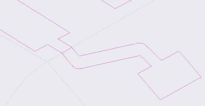
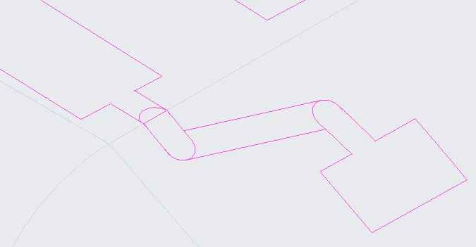
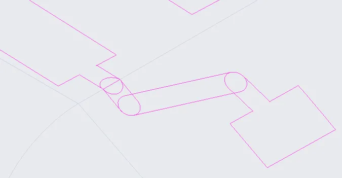
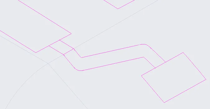
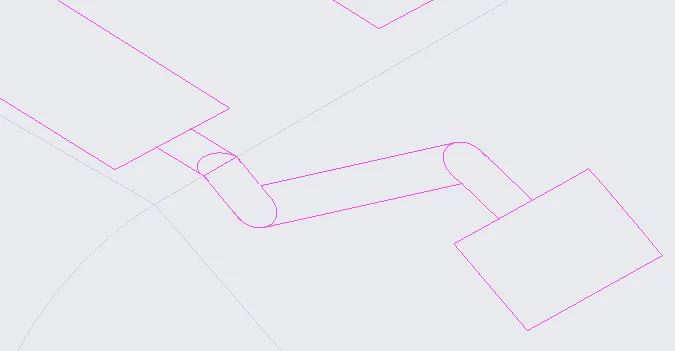
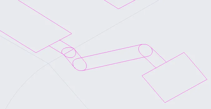
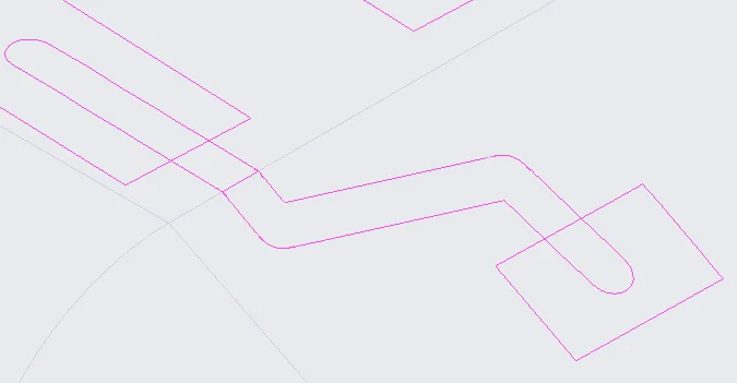
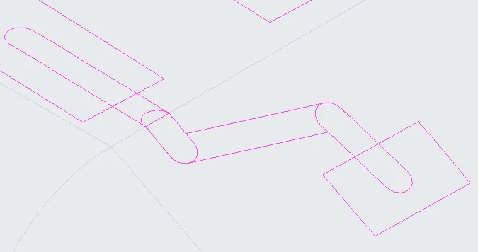
You can also control how the transitions between the conductive surfaces (merges) are handled in the exported file by changing the values of two Advanced Settings options. Search for merge in the Advanced Settings dialog to quickly locate the settings, as shown in the image below.

The effect of these settings on the export data is shown in the following table:
| |
TrackToTrackMergeMode=0 |
TrackToTrackMergeMode=1 |
TrackToTrackMergeMode=2 |
| PadToTrackMergeMode=0 |
 |
 |
 |
| PadToTrackMergeMode=1 |
 |
 |
 |
| PadToTrackMergeMode=2 |
 |
 |
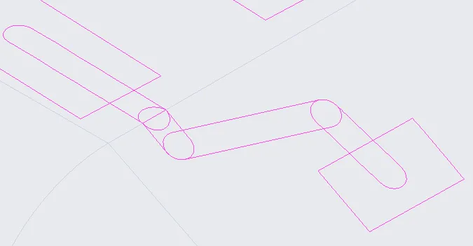 |
Note - the Laser Direct Structuring process typically requires the export data format associated with TrackToTrackMergeMode = 0 and TrackToPadMergeMode = 0.
Other Project Output Data
-
Project outputs that derive data from the schematic documents, for example, the Bill Of Materials, are available as normal.
-
Project outputs that rely on a PCB document, for example, a Draftsman assembly drawing, are not currently available for a 3D-MID document.
-
When exporting a 3D-MID design (File » Export » 3D-MID), a
txt pick and place file is generated in the same folder as the exported 3D-MID file (STEP, IGES, or Parasolid). This file contains information on the position of each component in the design: X, Y and Z coordinates of the component center and rotation vectors of the component. Rotation vectors depend on the component's rotation handle (visible when the component is selected):
-
Rotation Vector 1 is a vector opposite to the rotation handle.
-
Rotation Vector 2 is a normal vector to the surface in the component's location point.
-
Rotation Vector 3 is directed to the right side relative to the Rotation Vector 1 when looking from the top (opposite direction to the Rotation Vector 2).
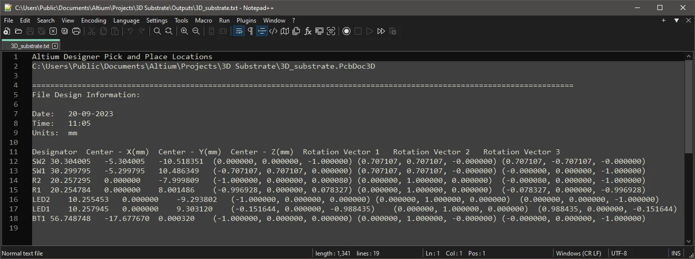
An example of a generated Pick and Place file for a 3D PCB
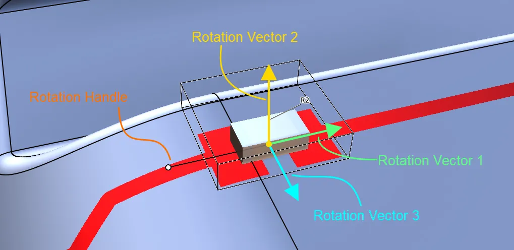
Arrangement of rotation vectors used for the Pick and Place file