New PCB Design Rules
Creepage Distance
This design rule flags a violation when the creepage distance across non-conductive surface and edge regions of the board, between the targeted signals, is equal to or less than the specified Creepage distance. The rule identifies the closest points on the targeted nets and checks the distance between them in the X-Y, and Z planes. It will trace around the edge of, and through, slots and holes in the board.

- Where the First / Second Object Matches - this is a binary rule, configure the First Object Matches settings to identify the net(s) that must maintain the specified creepage distance from other nets. Configure the Second Object Matches settings to identify the net(s) that the First Object must be kept the Creepage distance away from.
- Creepage Distance - a rule violation is flagged when any point on the First Object is equal to or less than this distance from any point on the Second Object.
 The creepage distance is calculated around and through board cutouts and un-plated pad holes.
- Ignore Internal Layers - ignore net objects placed on internal layers when testing the creepage distance.
Return Path Design Rule
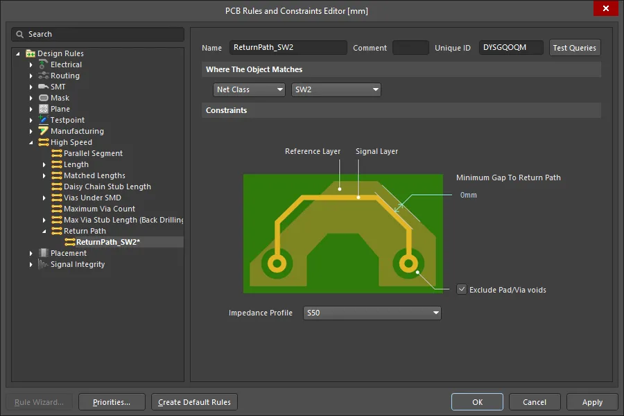
The Return Path design rule checks for a continuous signal return path on the designated reference layer above or below the signals targeted by the rule. The return path can be created from fills, regions and polygon pours placed on a signal layer, or it can be a plane layer.
The return path layers are the reference layers defined in the selected Impedance Profile.

- Where The Object Matches - configure to target the required signal net(s). The options are: (Net, Net Class, Layer, Net and Layer, Custom Query).
Max length Ignore - indicates the maximum allowable length of the conductor that can extend beyond the edge of the reference plane to where the conductor has an entry or exit point from this signal layer (eg via hole, contact pad, etc). During the check, the error will be ignored if the distance does not exceed the allowed value (default value is 0 mm).
- Exclude Pad/Via Voids - when enabled, openings in the return path created by the clearance around pads and vias that belong to the targeted net(s), are not flagged as violations.
- Minimum Gap to Return Path - indicates the minimum gap from the conductor edge to the outer edge of the return-path plane/polygon. The check is applied along the entire length of the conductor. An error will be flagged if the gap is equal to or less than the Minimum Gap to Return Path value (default value is 0 mm).
- Impedance Profile - select the applicable impedance profile for the nets targeted by this rule. The profile specifies which layer(s) provide the return path for the targeted signals. Once the layer stack has been selected the available signal layers and their respective reference layers will be shown in the grid region of the dialog.
 Enable the Violation Details for the Return Path rule to easily identify error locations.
