This page looks at performing Signal Integrity (SI) analyses. It covers setting up design parameters like design rules and Signal Integrity models, starting up Signal Integrity from the schematic and PCB editors, configuring the tests to be used in the net screening analysis, running further analysis on selected nets, terminating the signal line, setting preferences and working with the resulting waveforms.
With Altium Designer, you can analyze the Signal Integrity performance of a PCB from either the schematic or the PCB editors, evaluate net screening results against predefined tests, perform reflection and crosstalk analysis on selected nets, and display and manipulate the waveforms in the SimData editor.
The Signal Integrity Analysis capabilities are available through an Altium Designer Signal Integrity Analysis system extension, which is not installed with Altium Designer by default. The extension can be installed/removed or updated from the Altium Designer Extensions and Updates page (select the Extensions and Updates option from the system User menu –  ). When not installed, the Signal Integrity Analysis extension is located within the Purchased tab. Hover the cursor over the extension and click the
  icon at the top-right of its entry.

► See Extending & Updating Your Installation for more information on installing and managing Altium Designer extensions.
Signal Integrity Overview
Altium Designer includes pre-layout and post-layout Signal Integrity analysis capabilities. Altium Designer's Signal Integrity Analyzer uses sophisticated transmission line calculations and I/O buffer macro-model information as input for simulations. Based on a fast reflection and crosstalk simulator model, the Signal Integrity Analyzer produces accurate simulations using industry-proven algorithms.
Preliminary impedance and reflection simulations can be run from your source schematics prior to final board layout and routing. This allows you to address potential Signal Integrity issues, such as mismatched net impedances, before committing to board layout.
Full impedance, signal reflection and crosstalk analysis can be run on your final board (or a partially routed board) to check the real-world performance of your design. Signal Integrity screening is built into the Altium Designer design rules system, allowing you to check for Signal Integrity violations as part of the normal board DRC (Design Rule Checking) process. When Signal Integrity issues are found, Altium Designer shows you the effects of various termination options, allowing you to find the best solution before modifying your design.
Running a Signal Integrity Analysis from a Schematic Only Project
You can perform a Signal Integrity analysis on the design using only a schematic whenever there is no PCB as part of the project. The schematic must be part of a project, as analyses will not run on documents opened as Free Documents. There is no crosstalk analysis available because routed nets are required for this analysis.
When running in schematic only mode, default average track length and impedance can be defined using the Signal Integrity setup options. The Signal Integrity Analyzer also reads the PCB design rules from the schematic for the stimulus and supply nets. These rules can be added as PCB Layout directives or Parameter Set directives on nets in the schematic.
From the schematic editor, with the schematic open, select Tools » Signal Integrity from the menus. This will first allow you to setup any necessary signal integrity models and then show the Signal Integrity panel from where you can view initial results and perform further analysis.
Running a Signal Integrity Analysis from a PCB Project
When running a Signal Integrity analysis from a PCB document, the PCB must be part of a project along with the related schematics. Note that you could also run Signal Integrity from any of the schematic documents in the project and it will have the same effect as running it from the PCB. This will allow both reflection and crosstalk analysis to be performed.
From the PCB editor, select Tools » Signal Integrity which will proceed through the same process as that described above for the schematic only mode.
You can now have some (or none) of the schematic components in the PCB but any that have been placed must be linked with Component Links. This can be checked by selecting Project » Component Links. Note also that any unrouted nets will use the Manhattan length between pins to calculate a track length estimate for analysis purposes.
Before Running Signal Integrity
In order to run a successful Signal Integrity analysis of the design and obtain accurate results, the following has to be performed before running the analysis.
- Although each net can be screened to provide net and impedance data, not all nets can be analyzed for signal integrity characteristics (voltage and timing). In order to screen successfully for all characteristics, a net must contain at least one IC with an output pin and no other components. Resistors, capacitors and inductors for example will not provide simulation results on their own because of their lack of output pin to provide a driving source. It should be noted that when bidirectional nets are screened, both directions are simulated and the worst case result is displayed.
- The associated Signal Integrity model type for each component has to be correct. This is achieved via the Signal Integrity Model Assignments dialog or by manually setting the correct entry for the Type field in the Signal Integrity Model dialog, when editing the Signal Integrity model associated to the component placed on the schematic source document. If this entry is not defined, the Signal Integrity Model Assignments dialog will attempt to guess the type of the component based on its characteristics. If this entry is not defined, the type Integrated Circuit will be assumed. For more information, see Adding SI Models Using the Signal Integrity Model Assignments Dialog.
- There must be Supply Nets design rules. Generally, there should be at least two rules, one for power nets and one for ground nets. The scope for these can be either net or net class. Supply nets cannot be analyzed in Signal Integrity. For more information, see Signal Integrity Design Rules in Schematic or Signal Integrity Design Rules in PCB.
- A Signal Stimulus design rule may be set up. You only need a stimulus rule if you want to override the default stimulus, so this is generally not required.
- The layer stack for the PCB must be set up correctly. The Signal Integrity Analyzer requires continuous power planes. Split planes are not supported, so the net that is assigned to the plane is used. If they are not present, they are assumed, so it is far better to add them and set them up appropriately. The thickness of all layers, cores and prepreg must also be set correctly for the board. Use the Design » Layer Stack Manager command to set up the layer stack in the PCB editor. When running Signal Integrity in the schematic only mode, a default two layer board with two internal planes is used. You could create a blank PCB with a layer stack set up if more control was required. Refer to the Defining the Layer Stack page to learn more.
The characteristics of a signal, such as the voltage level, are determined by the model assigned to the output pin in the net under test. Pin models are assigned as part of the component model assignment process, and these component-level model assignments can be retained by updating the schematic. An individual pin model can also be overridden, for example by double-clicking on a pin in the Signal Integrity panel - note that these pin-level reassignments are not retained between editing sessions.
Adding SI Models Using the Signal Integrity Model Assignments Dialog
The simplest way to add signal integrity models to your design is to use the Signal Integrity Model Assignments dialog.
-
Select Tools » Signal Integrity from the menus. If you are just starting signal integrity on a project and there are components which do not have signal integrity models attached, you will be prompted by the Errors or warnings found dialog to set up the model assignments using the Signal Integrity Model Assignments dialog.
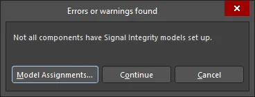
The Errors or warnings found dialog

The Signal Integrity Model Assignments dialog
Alternatively, if you have clicked Continue and the Signal Integrity panel is visible, it is possible to enter the Signal Integrity Model Assignments dialog at any time by clicking the Model Assignments button in the panel. Note that doing so will cause all results to be cleared and recalculated since any changes to model assignments invalidate any existing results.
If models have been already set up for all components, the SI Setup Options dialog will display. See Configuring the SI Setup Options for more information.
- If you click on Model Assignments in the Errors or warnings found dialog, the Signal Integrity Model Assignments dialog displays.
When run, the Signal Integrity Models Assignment dialog attempts to make educated guesses as to the necessary signal integrity model required for each component that does not contain a signal integrity model. All components, including those with models already defined (and the model information) will be displayed in the Signal Integrity Models Assignment dialog. Each component will be assigned a status as described in the following table.
| Status |
Definition |
| No match |
The Signal Integrity Model Assignments dialog was unable to find any characteristics linking this component to a particular type. It will likely need modification from the user to be set up correctly. |
| Low confidence |
The Signal Integrity Model Assignments dialog has selected a type for this component, but there was not strong evidence. |
| Medium confidence |
The Signal Integrity Model Assignments dialog has selected a type for this component and has reasonable confidence for the guess. |
| High confidence |
The Signal Integrity Model Assignments dialog has selected a type for this component and it fits most of the characteristics usually associated with this type of component. |
| Model found |
An existing model was found for this component. |
| User modified |
A component will change to this status once the user has modified it from the Signal Integrity Model Assignments dialog's initial guess. |
| Model added |
This status is used when the user has used the Signal Integrity Model Assignments dialog to modify the schematic document to save the new model. |
Modifying Component Models using the Signal Integrity Model Assignments dialog
- Select the component that you want to modify its model.
- Select the correct type. There are seven types of components for Signal Integrity – resistor, capacitor, inductor, diode, BJT, connector, and IC. The type of each component can be selected via a drop-down in the Type column or via the right-click menu.
- Set the value for a resistor, capacitor or inductor. If possible, the Signal Integrity Model Assignments dialog will attempt to place the correct value for the component in this column based on the comment field and parameters on the component. If this requires modification (or is not present), this should be done at this point. The special case of part arrays (such as resistor arrays) is done via a separate dialog accessed by clicking in the column (see Manually Adding Signal Integrity Models to Components for more details).
- If the component is an IC, the choice of technology type is important as this will determine the characteristics of the pin models used in simulation. This can be selected via the drop-down list in the Value/Type column or accessed through the right-click menu (Change Technology).
- Finally, it may be necessary to specify more detail than allowed in the Signal Integrity Model Assignments dialog, such as for IBIS models. This can be achieved by selecting Advanced from the right-click menu. See Manually Adding Signal Integrity Models to Components for more details on this process.
Saving Models
Once models have been chosen for any or all of the components, the schematic documents can be updated to permanently store this information.
- Check the Update Schematic column in the Signal Integrity Model Assignments dialog for all components that are to be updated. Then click the Update Models in Schematic button.
- All new Signal Integrity models (or modified existing ones) for each selected component will be added to the schematic documents. The schematic documents will need to be saved later.
It is not necessary to save models to proceed with the Signal Integrity analysis process. If models are not saved, the analysis will proceed with all models configured as they are currently shown in the Signal Integrity Model Assignments dialog. However, the next time the Signal Integrity tool is used, any changes will have been lost.
Manually Adding Signal Integrity Models to Components
To add a Signal Integrity model to a schematic component:
- For a placed component in the schematic editor – select the component and open the Properties panel.
- For a component being edited in the schematic symbol editor – make the required component active by selecting its entry in the SCH Library panel and open the Properties panel.
Click the Add button in the Parameters region of the Properties panel and select Signal Integrity. The Signal Integrity Model dialog will open.

Set up your model and click OK.
Setting Up Passive Components
When setting up parts such as resistors and capacitors, it is usually sufficient to enter a type and a value. The value can be entered in the Value field and can be set as a parameter for the whole component.
There is also support for components like resistor arrays. This can be achieved by, after selecting the component type, clicking the Setup Part Array button in the Signal Integrity Model dialog. The Part Array Editor dialog allows the connections between pins and the value/model for those connections to be configured.

The Part Array Editor dialog
Setting Up an IC
There are several alternatives when setting up an IC type model.
-
After selecting the type (IC), it is sufficient to select a technology type. This will ensure that when simulating this component, the appropriate pin models for that technology will be used. The full list of available technologies is in the collapsible section below.
Available Technology Types
| Technology Type |
Description |
| ABT |
Advanced Bipolar CMOS Technology |
| AC |
Advanced CMOS |
| ACT |
Advanced CMOS with TTL inputs |
| AHC |
Advanced High Speed CMOS |
| AHC_50 |
Advanced High Speed CMOS 5.0V |
| AHCT |
Advanced High Speed CMOS with TTL inputs |
| AHCT_50 |
Advanced High Speed CMOS 5.0V with TTL inputs |
| ALS |
Advanced Low Power Schottky |
| ALVC |
Advanced Low Voltage CMOS |
| AS |
Advanced Schottky |
| BCT |
Bipolar CMOS Technology |
| BTL |
Backplane Transceiver Logic/Futurebus+ |
| CMOS |
CMOS |
| F |
FAST |
| FCT |
FAST CMOS Technology |
| GTL |
Gunning Transceiver Logic |
| GTL_LVT |
Gunning Transceiver Logic Low Voltage |
| HC |
High Speed CMOS |
| HCT |
High Speed CMOS with TTL inputs |
| HLL |
High Speed Low Power Low Voltage CMOS |
| LS |
Low Power Schottky |
| LV |
Low Voltage High Speed CMOS |
| LVC |
Low Voltage CMOS |
| LVT |
Low Voltage BiCMOS Technology |
| S |
Schottky |
| STD_TTL |
Standard TTL |
| TTL |
TTL |
- If more control is required, it is possible to assign specific technologies or pin models to individual pins. This can be done by selecting from the drop-down lists for the pins in the pin list at the bottom of the Signal Integrity Model dialog. Note that any changes here will override the base technology for the component.
Importing IBIS Files
Another important option is the ability to import IBIS files.
-
To use an IBIS (Input/Output Buffer Information) file to specify an IC model's input and output characteristics, click the Import IBIS button in the Signal Integrity Model dialog. Select the IBIS file from the Open IBIS File dialog and click Open. The IBIS Converter dialog displays.
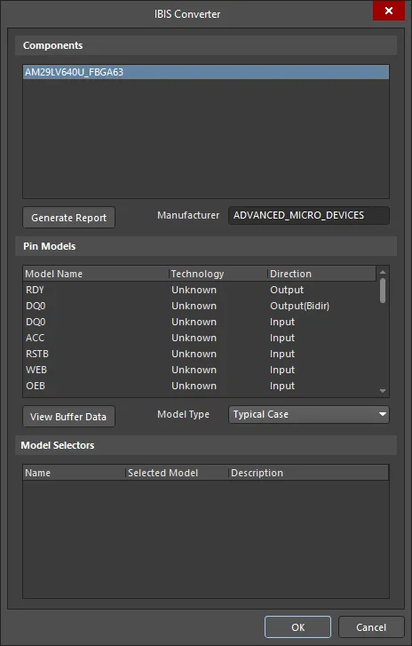
The IBIS Converter dialog
- Select the required component contained in the IBIS file. Altium Designer will read the IBIS file and import the pin models from the IBIS file into the library of installed pin models. If a duplicate model is found, you will be asked if you wish to override the existing model. Additionally, all pins on the component will have the appropriate pin model assigned as specified in the IBIS file.
- A report will automatically be generated stating which pins were successfully and unsuccessfully assigned. Further customization is possible by manually selecting the models for the appropriate pins as described above.
- Click OK to complete importing the IBIS information and return to the Signal Integrity Model dialog.
Editing Pin Models
It is possible to add or edit an existing pin model by specifying various electrical characteristics of that pin. Note that this is also available for other types such as BJTs, Connectors and Diodes.
-
To modify pin models, click the Add/Edit Model button in the Signal Integrity Model dialog if this button is available for that type. The Pin Model Editor dialog displays.
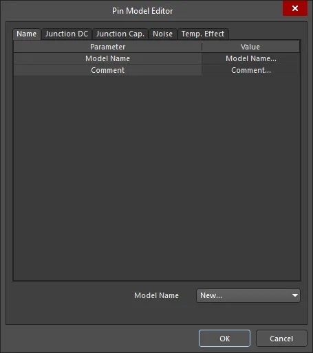
The Pin Model Editor dialog
- Click on New in the drop-down list for the Model Name.
- Make the necessary changes and click OK.
- If this is a new pin model, that model will now be available for selecting on the pins in this (and other) components.
Working with the Ibis Model Implementation Editor
To support third party tools that require dedicated IBIS models for their Signal Integrity simulations and cannot use Altium Designer's own Signal Integrity model format (referred to as SI Macro Models), Altium Designer incorporates a dedicated IBIS model implementation editor, allowing the IBIS model to be attached to the schematic component. So you can either:
- Import the IBIS pin models into the component pins during Signal Integrity Analysis (to be stored as Altium Designer SI Macro Models) as described above (see Importing IBIS Files), or
- Attach the IBIS model to the schematic component, as described below.
This feature supports all versions of IBIS model specification, up to and including version 4.0.
To add an IBIS model to a schematic component:
- For a placed component in the schematic editor – select the component and open the Properties panel.
- For a component being edited in the schematic symbol editor – make the required component active by selecting its entry in the SCH Library panel and open the Properties panel.
Click the Add button in the Parameters region of the Properties panel and select Ibis Model. The IBIS Model dialog will open.

Any number of IBIS model links can be defined for a schematic component, but only one can be the active model at any given time.
IBIS Model
Specify the name for the model – exactly as it appears within the .ibs file – and give the model link a meaningful name, perhaps describing what the implementation in this domain represents.
Alternatively, and especially if you are unsure of the name, use the Browse button to access the Browse Libraries dialog. Use this dialog to browse IBIS model files across all currently available libraries. Use the Find feature in this dialog if the required model files are not part of the currently available libraries.
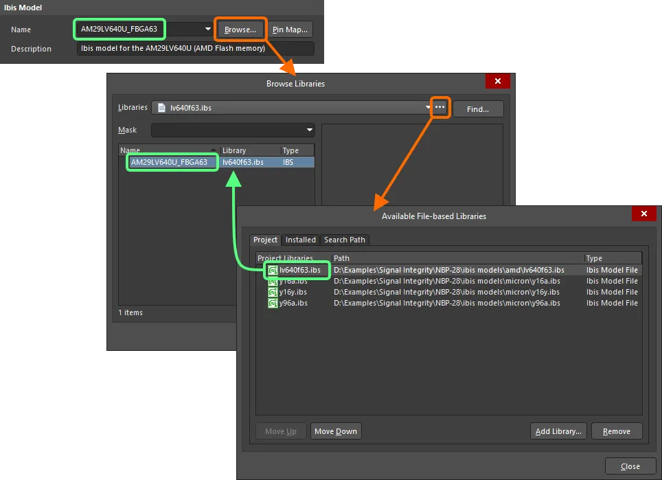
Specify the name of the model directly, or browse for it.
When browsing for an IBIS file, the Name drop-down will present all models, by name, defined within that file. Simply select the required one.
The mapping of schematic component pins to IBIS model pins is defined in the Model Map dialog, accessed by clicking the Pin Map button.

Verify component-to-model pin mapping in the Model Map dialog.
IBIS File Location
Options are available in this region of the IBIS Model dialog with which to specify how the software is to locate the model – provided the model name is defined:
- Any – all Available Libraries (project libraries, installed libraries and libraries found along defined search paths) are used to look for the model.
- File name – enter the full file name in which the model resides (e.g.,
lv640f63.ibs). All Available Libraries are used to look for the model. If not found here, the default library path (the Library Path field on the System – Default Locations page of the Preferences dialog) will be interrogated to see if the named file can be found there.
- File path – enter the full path/name of the file. Click the Choose button to browse to the file. This option will always find the model, since it is explicit (provided of course the file remains in that directory!).
- Integrated/Database Library – post-placement, if the component is placed from an integrated or database library, the model can be sourced directly from that same library, provided the library is part of the Available Libraries set.
If successfully located, indication of where the model was found will be presented.

Specify how to find the IBIS model.
Pin Models
This region of the dialog presents a view-only listing of the pin models defined for the chosen IBIS model. You can however change the Model Type from the default Typical Case, to either Strong Case or Weak Case respectively.
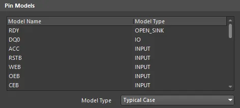
Pin Models for the chosen IBIS model.
Model Selectors
The Model Selectors region of the dialog will be populated if the chosen IBIS model has model selectors in it. This allows you to choose which model to use (e.g., a pin might have models for different voltage levels; 3.3V, 5V, etc.).
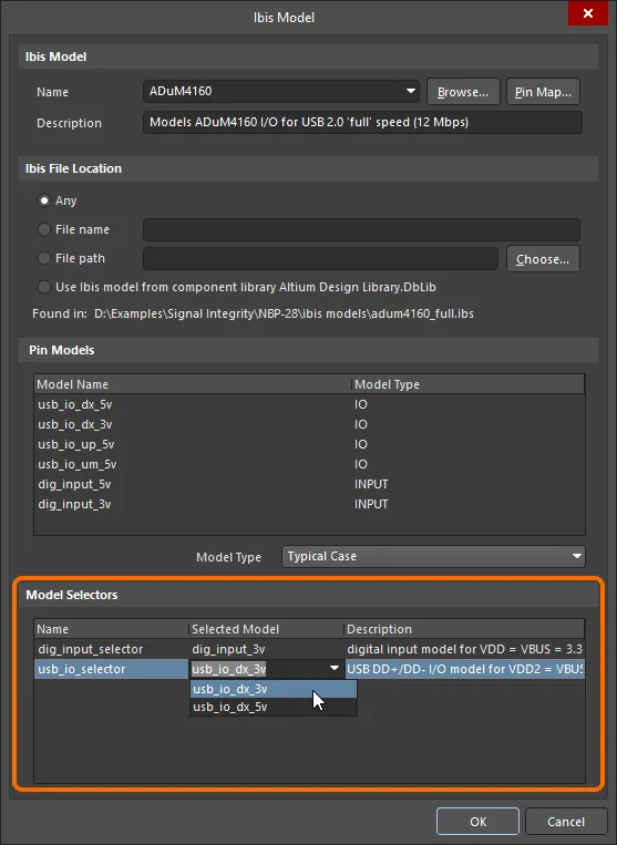
Example IBIS model with defined model selectors.
Signal Integrity Design Rules in Schematic
PCB-specific design rules for Signal Integrity can be defined in the schematic if they are added as parameters.
Supply Nets Design Rule
For Signal Integrity analysis, a PCB rule should be added to identify the supply nets and their voltage by using the Parameter Set directive. To add the supply nets design rule in the schematic:
- Place the Parameter Set directive (Place » Directive » Parameter Set) on the appropriate net.
- When the placed directive is selected, click the Add button in the Parameters region of the Properties panel and select Rule from the drop-down menu.
- The Choose Design Rule Type dialog will open where the rule type can be chosen. Scroll down to the Signal Integrity rules and select Supply Nets then click OK.
- The Edit PCB Rule (From Schematic) - Supply Nets dialog displays. Enter the voltage for this supply net and click OK. The rule entry will be listed in the Properties panel.

Signal Integrity design rules can be added right in schematics using the Parameter Set directives.
After transferring the design to PCB layout, the rule is added to the PCB design rules (available for viewing and editing in the PCB Editor from the PCB Rules and Constraints Editor dialog accessed using the Design » Rules command).
Note that in the schematic editor, the scope of the rule (the set of objects that the rule will target) is defined by where the parameter is added, e.g. on a wire or pin. In the PCB Editor, the scope of a rule is defined within the rule itself.
Signal Stimulus Design Rule
The other design rule that can be set up from within the schematic editor is the Signal Stimulus rule. When this rule is run, the stimulus is injected at each output pin on the net being analyzed. This requires a design rule that uses a scope of 'all', so you need to create a sheet parameter for this rule. If you do not set up this rule, the default rule options are used.
- When no object is selected in the schematic sheet, open the Properties panel. On the Parameters tab of the panel, click the Add button and select Rule from the drop-down menu.
- The Choose Design Rule Type dialog will open where the rule type can be chosen. Scroll down to the Signal Integrity rules and select Supply Nets then click OK.
- The Edit PCB Rule (From Schematic) - Signal Stimulus dialog displays. Choose the stimulus kind, start level and times, then click OK. The rule entry will be listed in the Properties panel.
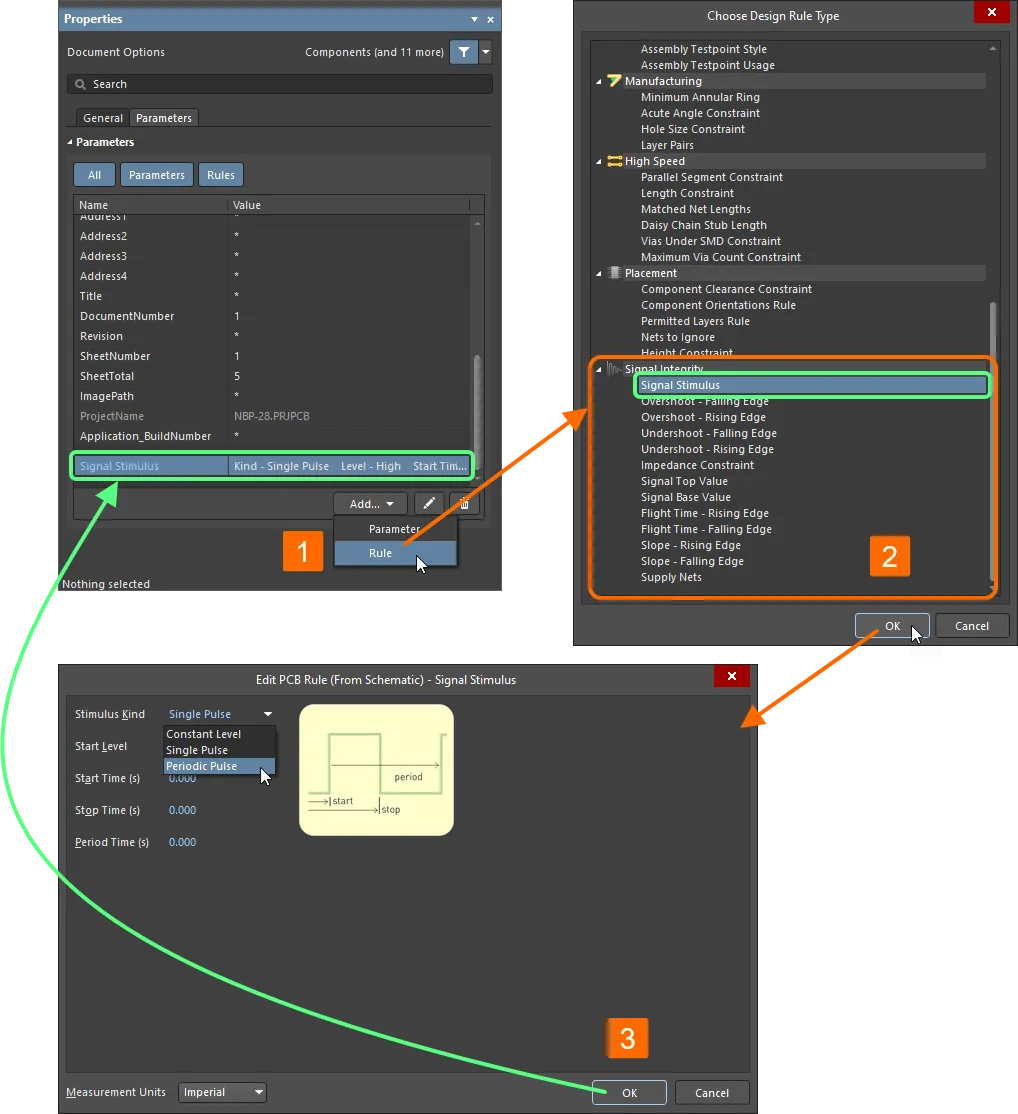
A Signal Integrity design rule can be added as a schematic sheet parameter.
Signal Integrity Design Rules in PCB
Signal Integrity parameters, such as overshoot, undershoot, impedance and signal slope requirements, can be specified as standard PCB design rules. Select Design » Rules in the PCB Editor to access the PCB Rules and Constraints Editor dialog where you can set up these rules. You can also set up these rules using parameters in the schematic editor and they will appear in the PCB Rules and Constraint Editor dialog after transferring the design to PCB layout.
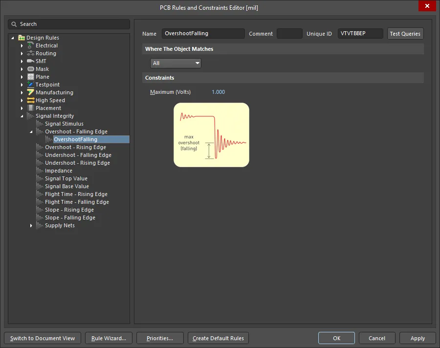
The PCB Rules and Constraint Editor dialog when browsing an Overshoot - Falling Edge design rule
These rules have two purposes. One is when running the standard DRC checks from within PCB – the board can be checked against these rules using the standard screening analysis. The second use for these rules is when using the Signal Integrity panel. These rules can be configured and enabled as tests and the panel will graphically display which nets have failed which tests.
Configuring the SI Setup Options
When you select Tools » Signal Integrity and all components have models assigned, the SI Setup Options dialog displays the first time you run this command on an open project.
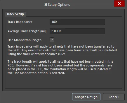
The SI Setup Options dialog
-
Set the track impedance and average track length as required. These routing characteristics are only required if there are any nets not yet transferred to a PCB or unrouted nets in the PCB.
Note that the Supply Nets and Stimulus tabs only display in schematic-only mode.
- Click on Analyze Design to run the initial default screening analysis and display the Signal Integrity panel from where you can further select the nets to analyze for reflection or crosstalk.
Four default tolerance rules and any Signal Integrity rules set in the schematic or PCB are all enabled and run the first time the design is analyzed. These tolerances can be set later in the Signal Integrity panel by clicking the Menu button and selecting Set Tolerances.
Signal Integrity Setup Options in Schematic Only Mode
If there is no PCB available in the project, you can change the SI setup options at any time by clicking the Menu button in the Signal Integrity panel and selecting Setup Options. The SI Setup Options dialog displays.
The Track Setup tab allows configuration of the default length of tracks when simulating. This is not used when a PCB is present as PCB uses width rules, i.e. if the Use Manhattan length option is disabled, PCB uses this value. Set the Track Impedance in this tab as well.
Click the Supply Nets and Stimulus tabs to display and enable net and stimulus rule information. These tabs allow another interface for defining these characteristics other than the normal method of providing rules on the PCB or schematic.

The tabs of the SI Setup Options dialog when accessed in schematic only mode
Using the Signal Integrity Panel
After performing any initial setup, the Signal Integrity panel will be loaded with data from the screening analysis that has just been run. The results of this analysis and a display of which nets have passed the various tests are displayed in the list on the left-hand side of the panel. The problematic nets can then be analyzed in greater detail by running fast reflection and crosstalk analyses. The ability to add virtual terminations allows you to ascertain what additional circuitry need be added to the design to resolve these problem areas and hence obtain the most efficient signal integrity performance.

The Signal Integrity panel is used to configure and control the signal integrity analysis process.
- Note that there is only one copy of this panel in the system so running Tools » Signal Integrity again will clear the existing panel and reload it with a new set of results. This may be used to refresh the results after making changes to either the PCB or schematic documents in the project or when starting to analyze a new project.
- The Reanalyze Design button allows you to perform the screening analysis again for the current design and should be used if you have made any changes to the design documents. In this way, you are assured of having the most up-to-date results for your design. You do not need to reanalyze the design after adding/editing signal integrity design rules as the screening results are compared against the enabled rule tolerances in real time.
Viewing the Screening Results
The initial screening analysis provides a fast simulation of many nets to enable you to get more information and identify critical nets for closer examination, such as detailed reflection and/or crosstalk analysis. The left-hand side list displays the results of this analysis. in tabular format. For each net in the design, the following column information can be displayed:
|
Net
|
The net name and a graphical representation of its status. This column is permanently displayed.
|
|
Status
|
A textual representation of the net's screening analysis status. This column is displayed by default.
|
|
Analysis Errors
|
Information as to why a net can't be analyzed.
|
|
Base Value
|
The voltage that the signal on the net settles to in the low state.
|
|
Falling Edge Flight Time
|
The time it takes for the signal on the net to fall to the threshold voltage, less the time it would take for a reference load (connected directly to the output) to fall to the threshold voltage.
|
|
Falling Edge Overshoot
|
The maximum overshoot (ringing below the base value) on the falling edge of the signal. This column is displayed by default.
|
|
Falling Edge Slope
|
The time it takes for the signal on the net to fall from the threshold voltage (VT), to a valid low (VIL).
|
|
Falling Edge Undershoot
|
The maximum undershoot (ringing above the base value) on the falling edge of the signal. This column is displayed by default.
|
|
Length
|
The total net length (sum of all routed track segments in the net).
|
|
Impedance
|
The average impedance for the net (in Ohms). This is the average of the impedance of each track segment, weighted by its length.
|
|
Rising Edge Flight Time
|
The time it takes to drive the signal on the net to the threshold voltage, less the time it would take to drive a reference load (connected directly to the output) to the threshold voltage.
|
|
Rising Edge Overshoot
|
The maximum overshoot (ringing above the top value) on the rising edge of the signal. This column is displayed by default.
|
|
Rising Edge Slope
|
The time it takes for the signal on the net to rise from the threshold voltage (VT), to a valid high (VIH).
|
|
Rising Edge Undershoot
|
The maximum undershoot (ringing below the top value) on the rising edge of the signal. This column is displayed by default.
|
|
Routed
|
Shows whether the net is routed (full or partial) in the design (True) or totally unrouted (False).
|
|
Top Value
|
The voltage that the signal on the net settles to in the high state.
|
Use the Menu button or right-click in the table to access the Show/Hide Columns sub-menu, from where you can enable/disable the display of data columns as required.
Each net can be in one of three categories: Passed, Failed or Not Analyzed.
 |
A Passed net had all values inside the bounds defined by the tests. |
 |
A Failed net had at least one value outside the defined tolerance levels. Any values that are failed are colored in yellow. |
 |
A Not Analyzed net could not be screened for some reason. To view the reason, enable the Analysis Errors column. |
Failed Nets
Common reasons for a failure to analyze a net in screening include containing a connector, diode or transistor, and no output pins or multiple output pins. When nets are screened which contain bi-directional pins and there is no dedicated output pin in the net, each bi-directional pin is simulated separately as an output pin. The worst-case result from these simulations is displayed.
Note that even though a net could not be analyzed for screening, it may still be able to be checked in reflection and crosstalk simulations. For a net containing a connector, you can simulate the connector using an equivalent impedance model added to this net.
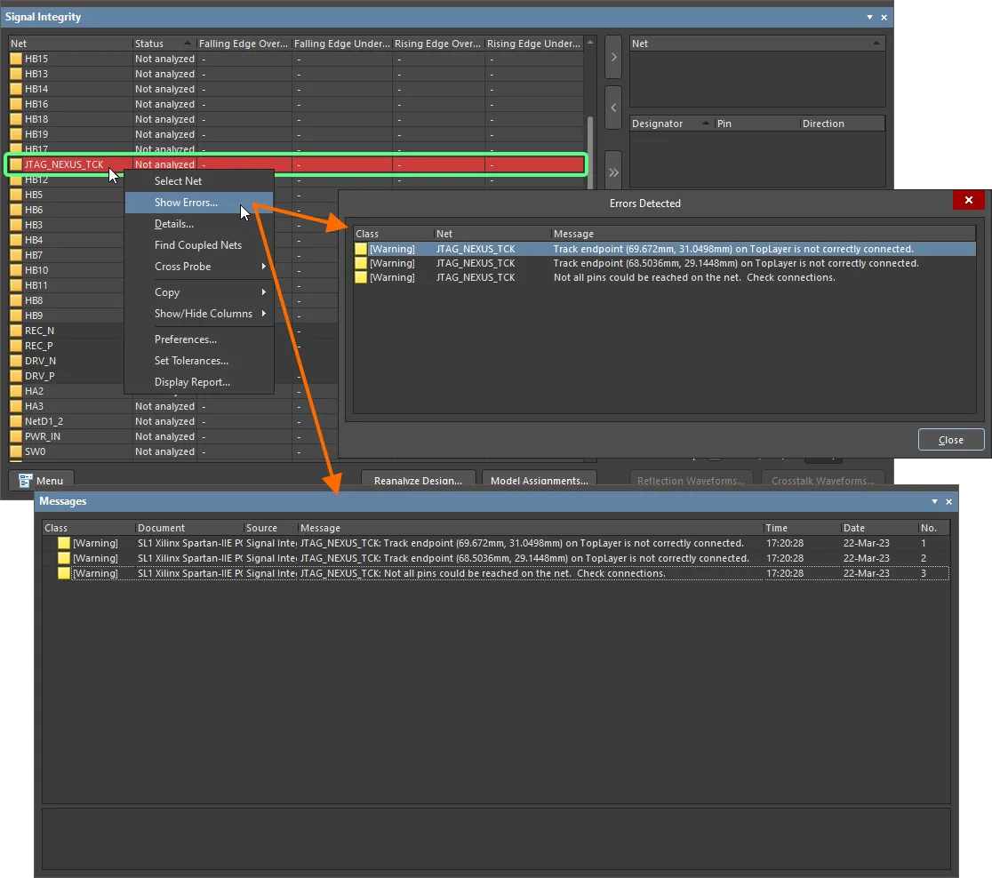
It is possible for nets to have other errors that will lead to incorrect analysis results in both screening and further simulations. These nets will appear with their entire row entry colored in red. Also, nets that have been simulated (i.e. nets that are not yet routed on a PCB) are colored in light gray.
Checking Failed or Not Analyzed Nets
To view the cause of a Failed or Not Analyzed net:
-
If the entire row of a net is highlighted in red, select it and then right-click and select Show Errors. This also adds messages to the Messages panel, which can be cross-probed to repair any issues.
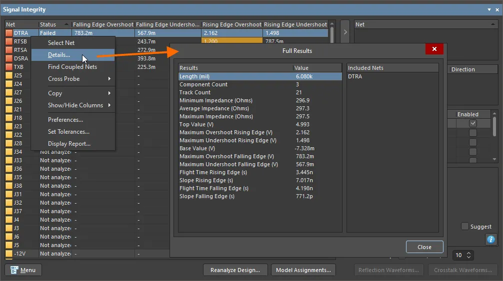
- To view all available information for a selected net, right-click and select Details. The Full Details dialog shows all of the screening analysis results that can be displayed in the results table, along with the following:
- Component Count – how many components have pads that connect to the selected net.
- Track Count – how many individual routed track segments comprise the total routed net.
- Minimum Impedance (Ohms) – the minimum impedance for the net, considering the individual impedances of all track segments in the net.
- Maximum Impedance (Ohms) – the maximum impedance for the net, considering the individual impedances of all track segments in the net.
-
Select Cross Probe from the right-click menu (or click Menu) to cross probe to the selected net on either the schematic or the PCB.
Use the F4 shortcut key to toggle display of the Signal Integrity panel (and other panels that are currently in 'floating' mode) to quickly switch between the panel and your design.
- Display which nets are coupled to either a single net or a group of nets by selecting the desired nets and then right-clicking and selecting Find Coupled Nets. This will select all nets that are coupled to these selected nets. The criteria for which nets are considered coupled can be configured in the Signal Integrity Preferences dialog (accessed by clicking the Menu button and selecting Preferences in the Signal Integrity panel).
- Useful information can be copied to the clipboard and pasted into other applications for further processing or reporting. Select the nets required and choose Copy from the right-click menu. Additionally, the displayed information can be customized by selecting which columns will be shown using the Show/Hide Columns command from the right-click menu.
- A report highlighting the results generated by the analysis is also available by selecting Display Report from the right-click menu in the Signal Integrity panel. This opens the report file
Signal Integrity Tests Report.txt in the Text Editor and adds it to the project.
Setting Preferences
You can specify various preferences that apply to all the analyses that you have defined. These include general settings, integration method and accuracy thresholds. Any changes made to the preferences will apply to all projects.
Click the Menu button in the Signal Integrity panel and select Preferences to open the Signal Integrity Preferences dialog.
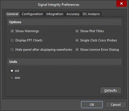
The Signal Integrity Preferences dialog
All Signal Integrity preferences can be returned to their defaults by clicking on the Defaults button in the dialog.
- Use the General tab to set the error handling options that show hints and/or warnings when errors exist in the design that relate to performing a Signal Integrity analysis. Any hints or warnings encountered will be listed as messages in the Messages panel. If the Show Warnings option is enabled and warnings exist, a warning confirmation dialog will appear when trying to access the Signal Integrity panel. Additionally, you can opt to hide the Signal Integrity panel after choosing to display waveforms. You can also define the default units for Signal Integrity measurements, whether plot titles and FFT charts will be displayed when the resulting waveforms are shown in the SimData editor.
- The Configuration tab defines various simulation-related thresholds, such as the maximum distance between coupled nets and the minimum length to be considered a coupled section.
- The Integration tab defines the numerical integration method used for analysis. The Trapezoidal method is relatively fast and accurate but tends to oscillate under certain conditions. The Gear methods require longer analysis times but tend to be more stable. Using a higher Gear order theoretically leads to more accurate results, but increases analysis time. The default is Trapezoidal.
- The Accuracy tab in the Signal Integrity Preferences dialog defines tolerance thresholds and limit settings for various computational algorithms involved in the analysis.
- Use the DC Analysis tab to define tolerance thresholds and limit settings for various parameters associated with DC Analysis.
Setting Tolerances
Default overshoot and undershoot tests are defined as these are probably the best characteristics to use in determining which nets may be the most problematic. Four default tolerance rules and any Signal Integrity rules set in the schematic or PCB are all enabled and run the first time the design is analyzed. To enable or disable these rules, click on the Menu button in the Signal Integrity panel and select Set Tolerances. The Set Screening Analysis Tolerances dialog displays.
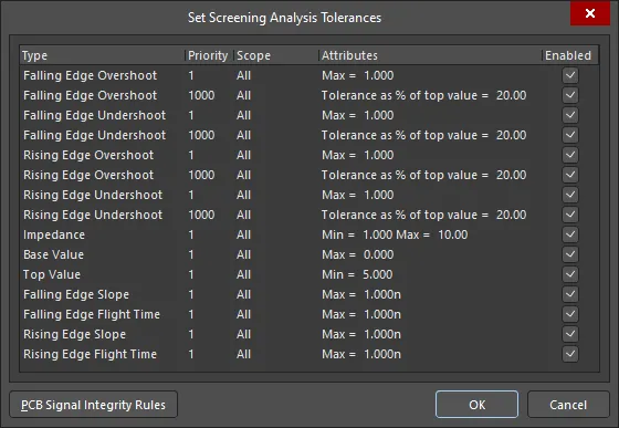
The Set Screening Analysis Tolerances dialog
Click on the Enabled checkbox next to a rule type to enable that rule to run when the design is analyzed.
Click on PCB Signal Integrity Rules (if not in schematic only mode) to open the PCB Rules and Constraints Editor dialog where you can add or modify any Signal Integrity rules required. Click OK until you return to the Signal Integrity panel.
Preparing Analyses
Before running the analyses, the nets to further analyze must be selected. You can also edit buffers to view or change the component part technology and pin properties and add terminations to nets if required.
Selecting Nets to Analyze
To perform further analysis on nets (reflection and/or crosstalk) the nets must be selected in the right-hand list of the Signal Integrity panel. Double-click on a net in the left-hand list to select it and move it to the right-hand list. Alternatively, use the arrow buttons to move nets to and from this selected state. You can multi-select nets in the left-hand list by holding down the Shift or Ctrl keys.
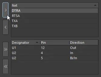
You can cross probe to the selected net(s) on the relevant schematic or PCB document by selecting the Cross Probe options from the right-click menu. The target document will be made active in the design space and the selected net(s) will be displayed in accordance with the highlighting methods defined on the System – Navigation page of the Preferences dialog.
Once nets are in this selected state, it is possible to perform further configuration for them before running a simulation.
Setting Victim and Aggressor Nets
In the case of Crosstalk analyses, it is necessary to set a victim or an aggressor net. Note that due to the nature of the analysis, this functionality is only available when two or more nets have been selected (moved to the right-hand list).
Select a net in the right-hand list of nets, right-click and select Set Aggressor or Set Victim as required. The status of the nets is updated. To unset the nets, select Clear Status from the right-click menu.
Setting the Direction of Bidirectional Pins
It is possible to set the direction of bidirectional pins in a given net. To set the direction, select the affected net in the top right-hand list. This will then display a list of pins for that net below. From the list of pins, change the in/out status for each selected bidirectional pin by right-clicking and choosing a status from the right-click menu. These in/out settings will be saved with the project for the next time you use this panel.
You can also cross probe to the pin/pad on the relevant schematic or PCB document by selecting the Cross Probe options from the right-click menu. The target document will be made active in the design space and the selected pin/pad will be displayed in accordance with the highlighting methods defined on the System – Navigation page of the Preferences dialog.
Editing Buffers
You may wish to view or change the component part technology and pin properties, such as input and output models and pin direction. You can only modify components that are attached to the currently selected net in the right-hand list. Using the Edit Buffer option under the right-click menu in the list of pins, gives access to the component's data dialog.
The dialog and options that appear will depend on the type of component the pin belongs to, e.g. resistor, IC, BJT, etc. The Integrated Circuit dialog shown is for an IC component type.
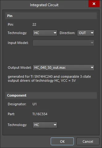
The Integrated Circuit dialog
Choosing a pin Technology and Direction will display a list of relevant input and/or output models to select from. Changes to the technology and direction are used locally in the analysis only and these will not be saved when the panel is reset.
The part Technology, Input Model and Output Model fields are context-sensitive. When you choose a component part technology, the default models of the part are taken from this technology. Note that if specific pin models have already been assigned (for example as part of importing an IBIS model), changing the component part technology will not re-assign pin models for those pins.
Note that you are really editing the properties of a pin rather than the whole component, even though you can change the component's technology. Any changes you make using the Edit Buffer command (or by double-clicking on a pin) will override any technology/pin model setup created when you set up the Signal Integrity model in the schematic.
Note that changes made using this approach are NOT retained between analysis sessions, the idea is that this feature is used to quickly change the assigned pin model to test what-if scenarios. If you want the assignments to be retained, edit the models assigned to the component instead of editing the pin models.
Terminations
The oscillations apparent on a signal waveform are due to multiple reflections on the associated transmission line (trace). These reflections, or 'ringing', occur most often in PCB designs because of driver/receiver impedance mismatch – usually where there is a low impedance driver and a high impedance receiver.
Getting good signal quality at the load would ideally mean zero reflections (no ringing). The level of ringing can be reduced to an acceptable level for the design using a termination.
The Signal Integrity panel incorporates a termination advisor, which enables you to insert 'virtual terminations' into a net at a location you define. In this way, you are free to test various termination strategies, without making physical changes to your board.

Termination simulations available are:
- Series Res
- Parallel Res to VCC
- Parallel Res to GND
- Parallel Res to VCC and GND
- Res and Cap to GND
- Parallel and Cap to GND
- Parallel Schottky Diodes
Each termination type can be enabled or disabled in the termination list. Multiple termination types can be enabled when performing reflection and crosstalk analyses - a separate set of waveforms will be produced for each. This allows you to determine the best termination to add to the design to achieve optimal signal quality on transmission lines and therefore reduce reflections (ringing) to an acceptable level.
When a reflection or crosstalk analysis is run, each enabled termination type will be tried and produce a separate set of waveforms. When the Serial Res termination is used, it will be placed on all output pins in the selected net. For other termination types, the termination will be placed on all input pins in the net.
To achieve the best results for the terminations, it will also be necessary to set the value of the parts involved based on the characteristics of the net.
- When a termination is selected, a diagram showing that termination is displayed below. This diagram will allow the setting of both minimum and maximum values for the resistors and capacitors used in the terminations.
- Minimum and maximum values are used when the sweep count (shown in the list of terminations) is set to a number greater than one.
- For more information about a termination type, select it and click the ? (Help) button. If you enable the Suggest option, suggested values will be calculated (according to the formula noted in the information popup for each termination type) and displayed in gray. You can accept these values or disable the Suggest option and enter your own values as required.
- If you want to run the analysis with a swept range of values for the termination components, ensure that the Perform Sweep option is enabled and set the number of Sweep Steps required when the analyses are run. The values used at each sweep of the analysis will depend on the minimum and maximum values entered and the value chosen in the Sweep Steps field (e.g., if Sweep Steps is set to 2, the first pass of the analysis will use the minimum value and the second the maximum). Note that a separate set of waveforms will be generated for each sweep for comparison purposes.
Placing a Termination on the Schematic
Once the waveforms have been created and the optimum termination detected, it may be desirable to place that termination directly on the schematic sheet. This can be achieved via the right-click menu in the Termination list. Note that any placement will only apply to the currently selected net.
If you wish to actually place the selected termination circuit on the schematic rather than just use it as a 'virtual termination':
- Right-click in the Termination section of the Signal Integrity panel and select Place on Schematic.
-
The Place Termination dialog displays, allowing the setting of various properties such as which library components to use for the termination parts, whether to use automatic or manual placement, whether to place on all applicable pins or just the selected pin and the exact values to be used for the parts. Click OK to continue.
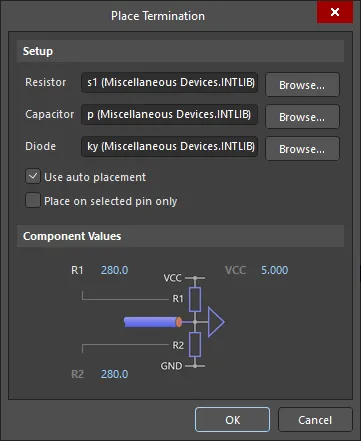
The Place Termination dialog
- The Signal Integrity Analyzer finds the source schematic document that the pin belongs to. Then, in a free space on the document, it will add the necessary parts with the correct values (resistors, capacitors or whatever is required) and the power objects. Connect this termination circuit to the appropriate pin in the schematic.
Note that it will still probably be necessary after this to wire the components correctly to the pin. Additionally, if there is a PCB involved as well, these will need to be synchronized and routed in the PCB. Synchronize the PCB to add these parts as well by selecting Design » Update PCB.
Running the Analyses
Once the nets have been configured as necessary (and any termination options chosen), click the Reflections or the Crosstalks button in the Signal Integrity panel to generate the waveforms.
-
For a Reflection analysis, one or more nets can be simulated. The number should be kept to a reasonable amount however, as analysis time will increase considerably when analyzing high numbers of nets.
The Signal Integrity Analyzer calculates voltages at nodes of a net using routing and layer information from the PCB and associated driver and receiver I/O buffer models. A 2D-field solver automatically calculates the electrical characterization of the transmission lines. Modeling assumes that DC path losses are small enough to be ignored.
-
For a Crosstalk analysis, at least two nets must be taken over. Two or three nets would normally be considered at any one time when performing a crosstalk analysis, usually a net and its two immediate neighbors.
The level of crosstalk (or the extent of EMI) is directly proportional to the reflections on a signal line. If the signal quality conditions are achieved and reflections are brought down to a near-negligible level through correct signal termination, i.e. the signal is delivered to its destination with minimal signal stray and crosstalk will also be minimized. See Terminations for more information.
Crosstalk analysis is only possible when performing post-layout signal integrity analysis from a PCB design document. This is because routed nets are required for this type of analysis.
After clicking a button, the analysis commences and a simulation data file (<ProjectName>.sdf) is generated. This file opens as a separate tab, displaying the results of the analyses in the SimData editor.
The generated SDF document comprises one or more tabs that correspond to the nets you have selected for analysis. Each tab contains a chart that can contain multiple wave plots. A wave plot can have multiple waveforms and a waveform represents the simulation data.
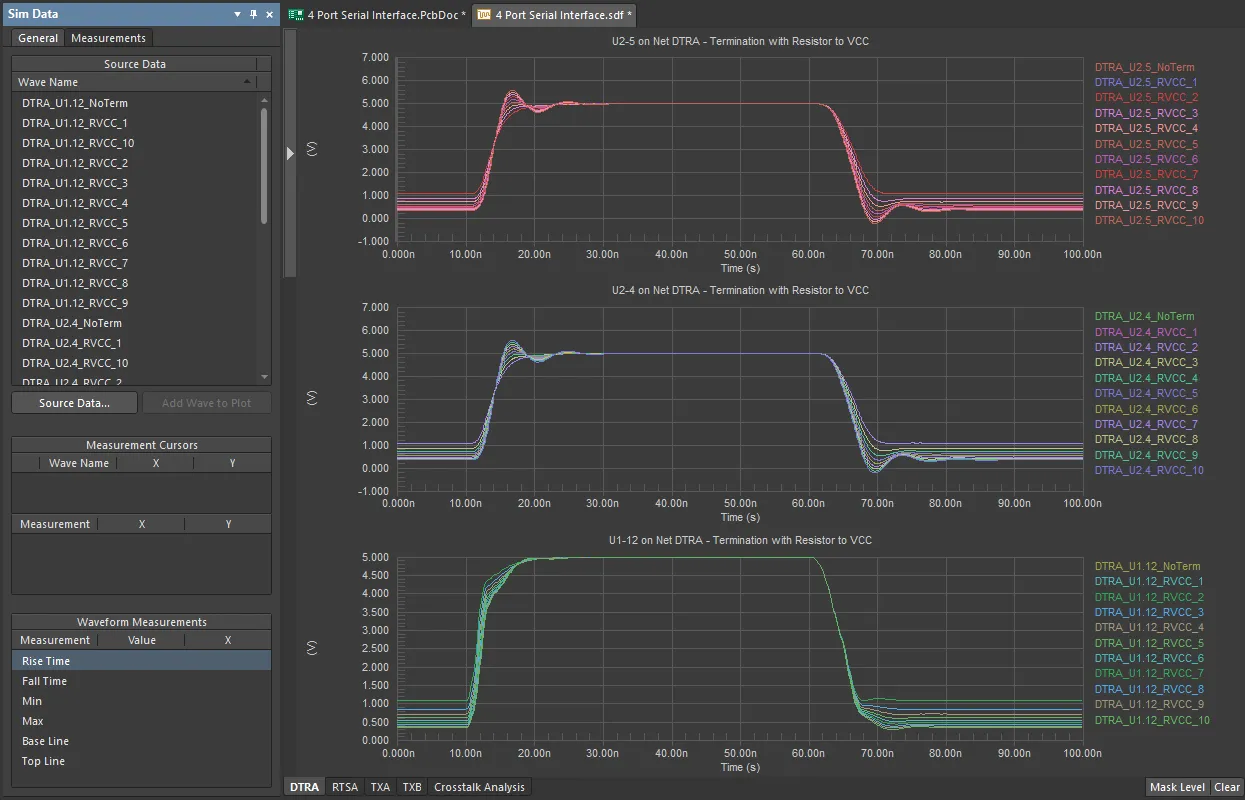
Accessing signal integrity analysis results. Click the tab at the bottom to access the results for each analysis type.
- The SimData editor is also used to work with simulation data generated by a run of the MixedSim analysis. Refer to the Working with Simulation Results – Charts, Plots and Waveforms page to learn more about working with charts, plots, and waveforms in an SDF document.
- Note that when running a signal integrity analysis, the extent of the generated plots' X-axis is determined by the Total Time (s) option, set on the Configuration tab of the Signal Integrity Preferences dialog (accessed from the Signal Integrity panel).
Reflection Analysis Data
For each net that has been selected, a chart is generated as the result of the simulation with its tab in the SDF document marked by the name of the net. The chart will contain waveforms for all termination options.
For a reflection analysis chart, the data displayed depends on:
- the number of pins in the net under test
- the specific termination types enabled (on the Signal Integrity panel)
- whether a sweep of the (virtual) termination component values is included as part of the analysis (again, enabled and defined on the Signal Integrity panel).
If you ran a reflection analysis with no termination components, a chart would contain one plot for each pin in the net under test. Each plot would contain one waveform – relating to the analysis of that pin with no termination used. For example, consider a reflection analysis for the net RTSB, which includes the following pins:
- U1 pin 12
- U3 pin 4
- U3 pin 5
With no terminations enabled, the following chart (plots and waveforms) would be created and displayed for this net. The waveform names are created based on the net name, the specific pin and the type of termination (in this case, no termination).
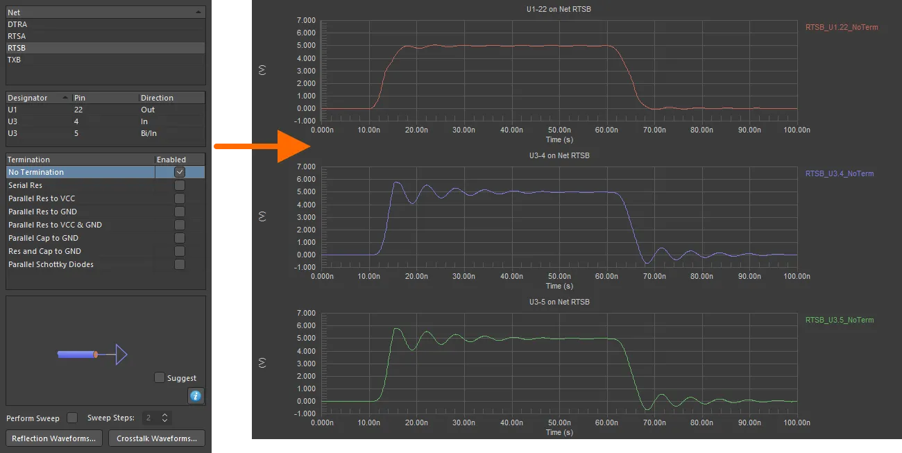
Reflection results – no terminations
If you were to enable specific termination types, without enabling a sweep of the values, additional waveforms would be added to each plot representing the results obtained by using each of those terminations. The image below shows, for emphasis, the case when all termination types are enabled.
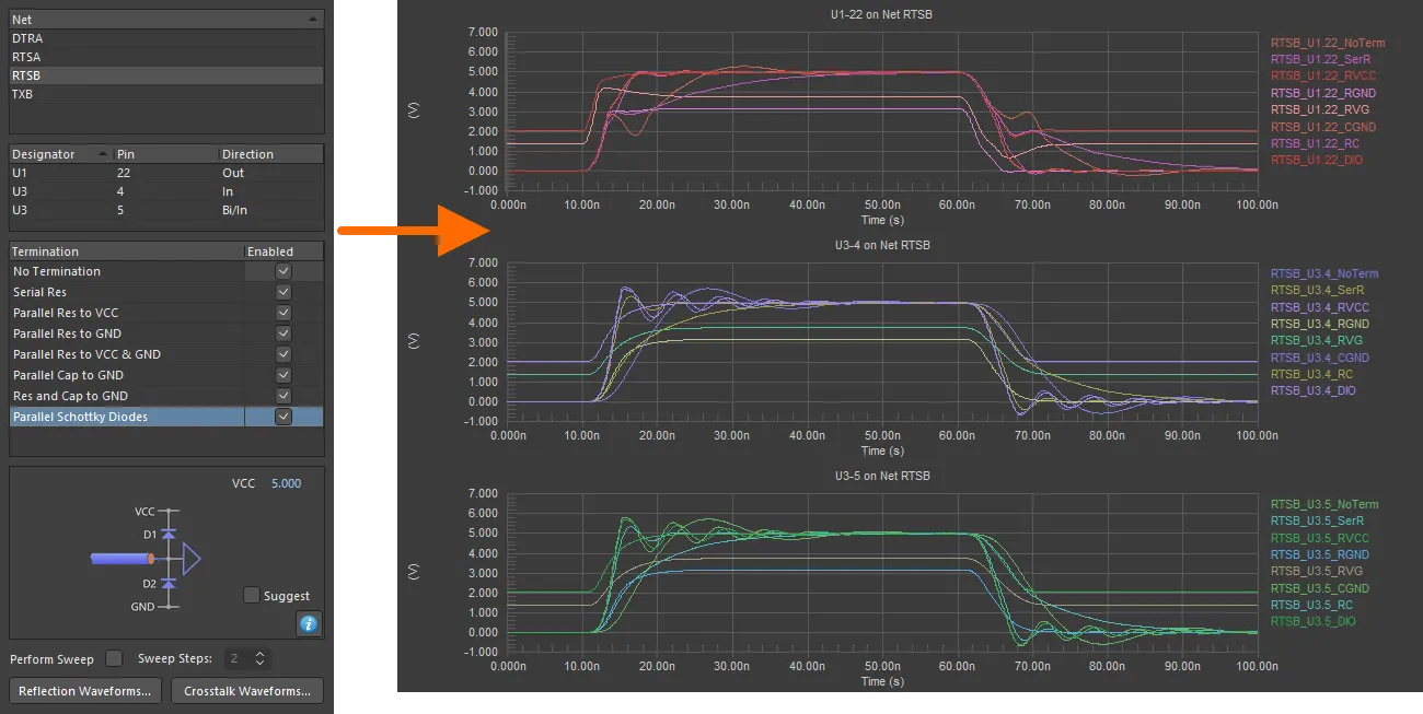
Reflection results – terminations enabled (no sweep)
If you enable terminations AND a sweep of the termination values (with two or more sweep steps), you will get a plot for each pin in the net under test, and for each enabled termination. The waveforms that are displayed within each plot will be those for each sweep step for that particular termination, as well as the no termination waveform (for comparison). The image below illustrates this display for our example RTSB net – with two termination types enabled (Serial Res and Parallel Res to VCC), and the sweep feature enabled with Sweep Steps set to 2.
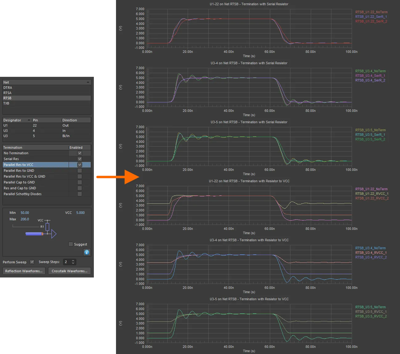
Reflection results – terminations enabled, with sweep.
Crosstalk Analysis Data
In a crosstalk analysis, all nets will be displayed in a chart named Crosstalk Analysis. The display of data for the crosstalk analysis chart is essentially the same as that for a reflection analysis chart. The only difference is that as there is only a single chart for this analysis type, it will contain a plot for each pin in each net considered in the analysis. The image below shows an example where two nets are considered in a crosstalk analysis – DTRA (set to be the Aggressor net) and RTSA (which defaults to being the Victim net). No specific termination types have been enabled.
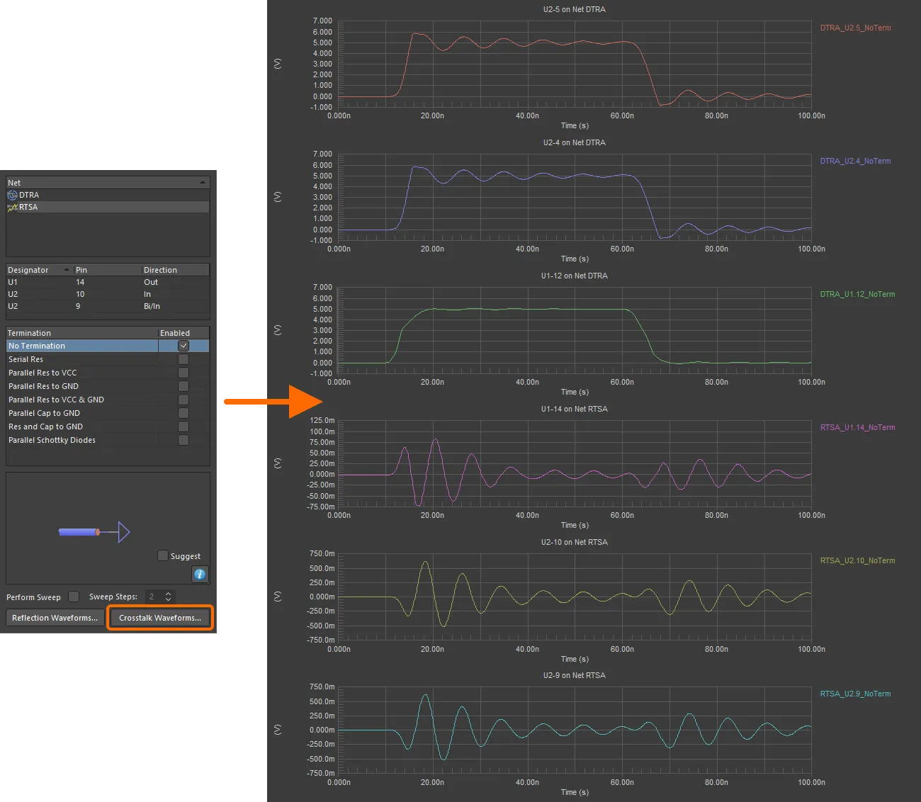
Crosstalk results – no terminations
Cross Probing to the PCB
If you have performed a post-layout signal integrity analysis of your design, the ability to cross-probe from a selected waveform to a PCB is available.
To cross probe, right-click on the required waveform name and choose the Cross Probe to <DocumentName>.PcbDoc command. The PCB document will be made active and the corresponding pin for the analyzed net will be highlighted, again in accordance with the Highlight Methods defined on the System – Navigation page of the Preferences dialog.
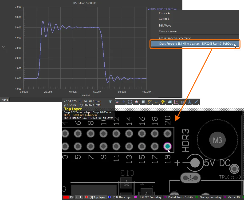
An example of cross-probing to a PCB, where pad 19 of component HDR3 – associated with net HB19 – is highlighted.
After Analyzing your Results
Once you have analyzed your results, you can experiment, for example, with various terminations to bring down any ringing on the selected nets. You may also need to make changes to your circuit or PCB and rerun your Signal Integrity analyses until the desired results are reached.
Note that as you run subsequent reflection and crosstalk analyses on different nets, the results will be added to the same simulation data file, appearing as new charts (tabs at the bottom of the SDF document).
