The most common schematic-to-PCB design task is keeping the schematic and PCB matched or synchronized. Whether you are transferring a captured design to a new PCB for the first time, or making changes to an existing design on either the schematic or PCB side, you need some way to keep the two sides in sync. Altium Designer includes powerful design synchronization capabilities that simplify the task of keeping the design synchronized, allowing the designer to keep their focus on the creative aspects of the design process.
 The synchronization process detects and resolves the schematic and PCB differences.
Design synchronization is performed directly between the schematic and PCB editors; there is no intermediate, netlist-like document used. The software uses a comparator engine to compare all aspects of the design, detailing the output as a list of differences. The designer decides which side should change to resolve the differences, and a set of Engineering Change Orders (ECOs) is created. When these are applied, the two sides of the design are back in sync.
There are two approaches to performing a synchronization:
-
Bi-directional synchronization, where differences can be updated in both directions simultaneously, using the Project » Show Differences command (as shown above). Refer to the Finding Differences section to learn more about this approach.
-
Single-direction synchronization, using the Design » Update PCB, or the Design » Update Schematic commands. Refer to the Performing a Direct Update section to learn more about this approach.
Before transferring the schematic information to the new PCB, it is essential that all the related libraries for both schematic symbols and PCB footprints are available.
What Can be Synchronized?
The synchronization process ensures that the component and connective data on the schematic, matches the component and connective data on the PCB. As well as the component and connective data, the synchronization process also ensures that other design constraints; such as net classes, component classes and design rules, are also in sync.
The inclusion of true components to the PCB editor means the PCB component can now hold all of the component data. This change means when a pre-Altium Designer 20.0 design is synchronized for the first time in Altium Designer 20.0, all component information that was not previously supported in the PCB component, will be added.
As part of these updates, the verification of footprint assignments has also been improved. In earlier versions, multi-part component footprint detection would use the first footprint detected in any sub-part of a multi-part component. With this update, the footprint assignments are checked across all sub-parts, and if they do not match, then the footprint assignment fails for that component during design synchronization. The schematic Footprint Manager can be used to examine and update the footprint assignments.
Configuring the Comparator Options
Dialog page: Options for PCB Project, Comparator tab
Exactly what schematic and PCB data gets compared, is configured in the Comparator tab of the Options for PCB Project dialog. Select Project » Project Options to open the dialog.
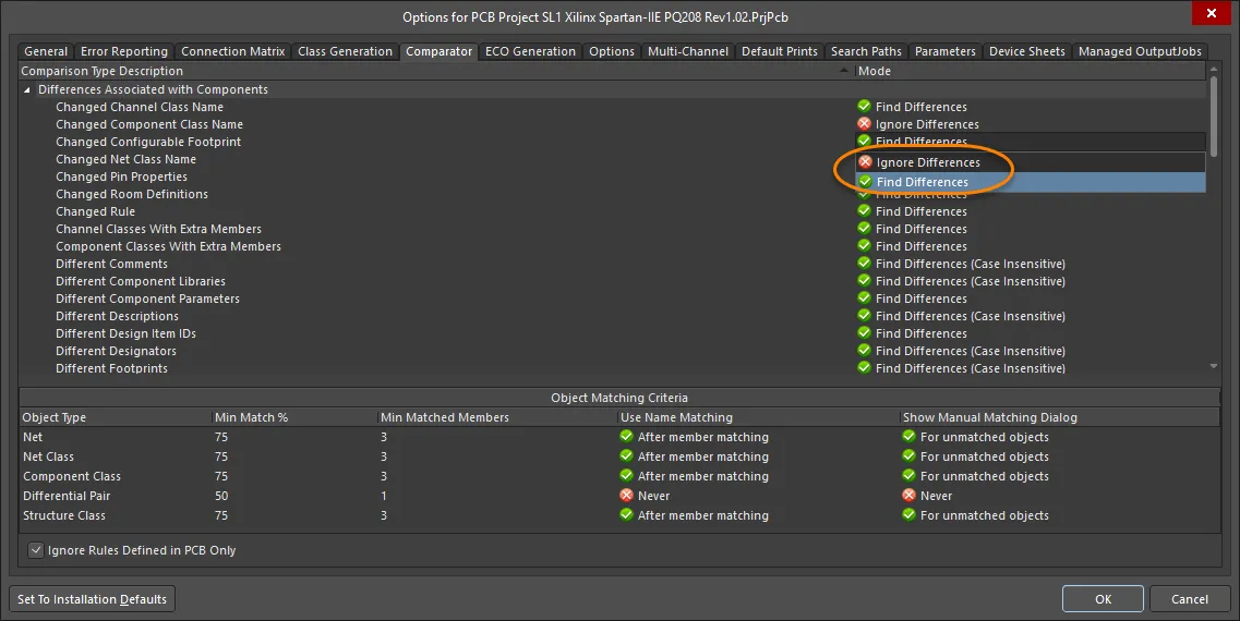
The comparator engine obeys the settings defined in the Comparator tab of the Options for Project dialog.
The main region of the dialog includes a large list of Comparison Types, such as Different Designators and Changed Net Name, which are grouped in 5 categories. The Mode column on the right includes a dropdown for each, where you select the mode of comparison, such as Find Differences or Ignore Differences. Text-type comparisons have a third option, to allow the comparison to be case-insensitive.
The default for a new project is to Find Differences for every comparison type, set the options as required for your project.
-
For schematic to PCB synchronization, all of the PCB related details can be synchronized.
-
For PCB to schematic synchronization, only changes made to the component designator, comment and footprint can be synchronized back to the schematic. The only net changes that can be synchronized are changes due to a pin or part swap operation - how this is carried out depends on how the pin/part swap options are configured. To learn more, refer to the Pin and Part Swapping page.
Across the bottom of the dialog there are options for setting the Object Matching Criteria. Matching is a sophisticated, multi-pass process that does not rely on simple exact string matching. To learn more, refer to the Matching the Nets and Classes section.
Note the Ignore Rules Defined in the PCB Only option down the bottom of the dialog, enable this to exclude the rules you have defined in the PCB, from the comparison process.
Synchronizing Net and Component Classes
Dialog page: Options for PCB Project, Class Generation tab
As well as component and connective data, you can also generate and synchronize classes and design rules when you perform a Design » Update PCB.
Synchronizing Design Rules
Design rules can be defined in the schematic, using a Parameter Set object. When a Parameter Set object is selected, the Properties panel or modal dialog includes a Rules region. Click the Add drop-down to add a design rule. The rule will be applied to the net / bus / harness / objects under the blanket, which the Parameter Set object is touching.
In the image below, a width constraint design rule is being applied to the USB_data net class (the net class is also defined as part of this Parameter Set, in the Classes region of the Parameters drop-down).
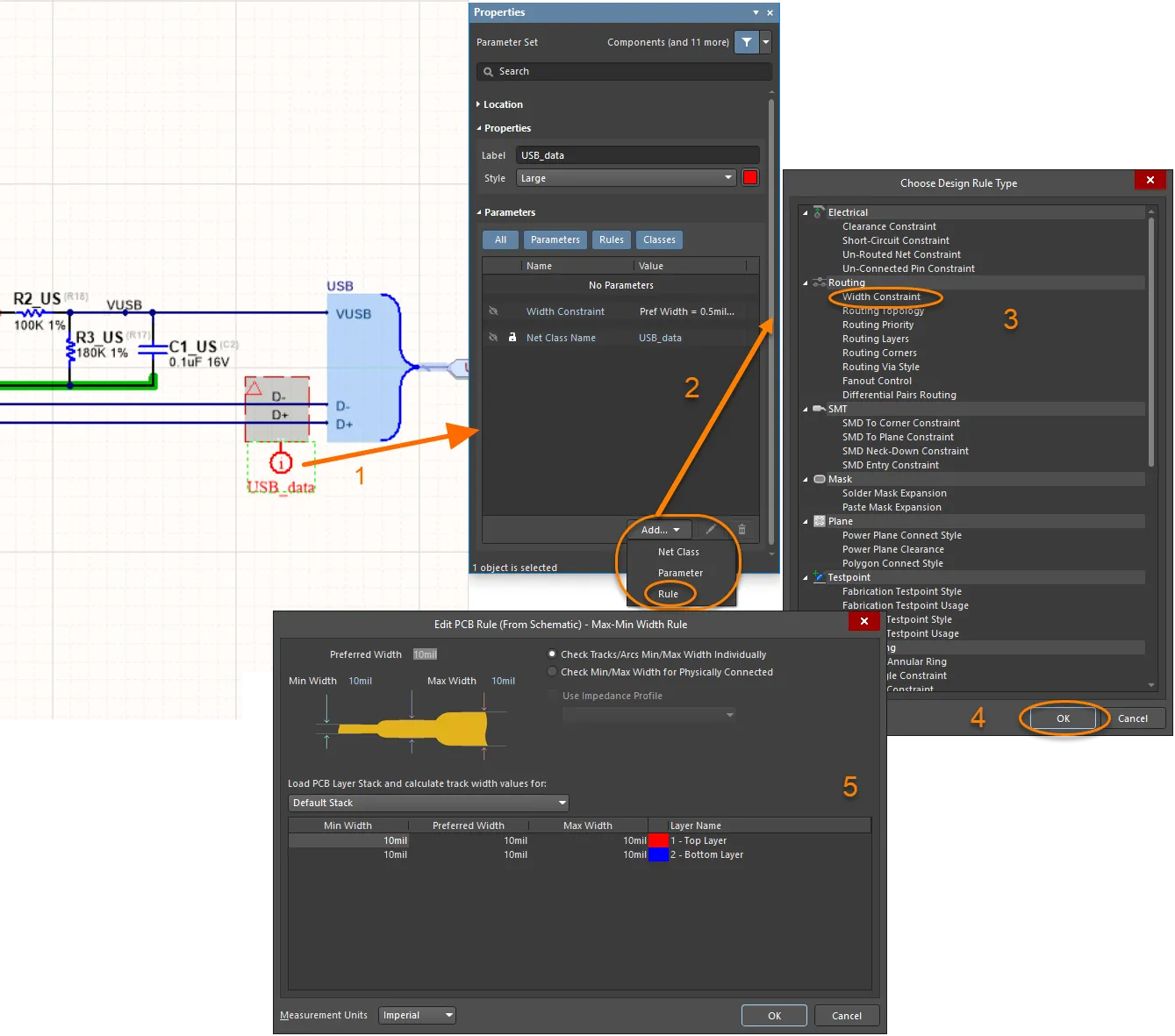
The Parameter Set is used to define a net class and a design rule, to the nets under the schematic blanket object. Note that the required measurement units are configured at the bottom of the Edit PCB Rule dialog.
Adding a Design Rule in the schematic
-
Attach a Parameter Set to the net / bus / harness / blanket (add a Net Class definition in the Parameter Set, if required).
-
Add a Rule definition in the the Parameter Set. This will open the Choose Design Rule Type dialog, as shown above.
-
Select the required Rule Type.
-
Click the OK button to open the Edit PCB Rule dialog.
-
Configure the PCB rule requirements as required. Note that the measurement units required for this PCB rule are selected at the bottom of the dialog.
In the Comparator tab of the Options for Project dialog, ensure that the required Rule type comparisons are enabled, to allow design rules to be added and updated in the PCB.
Each PCB rule that is created from a schematic rule definition is automatically named Schematic <RuleType>. If required, this name can be edited as it is not used for ongoing rule synchronization.
In both the image above and the image below, the design rule is defined in a Parameter Set object that is attached to a blanket. By including a Class definition in the Parameter Set object, a PCB net class will also be created, and because the class definition is present, the PCB rule will be scoped InNetClass('<PCB_NetClassName >').
In the image below you will notice that the Parameter Set object is displayed as a Differential Pair directive. This is a special type of Parameter Set object, placed using the Place » Directives » Differential Pair command.
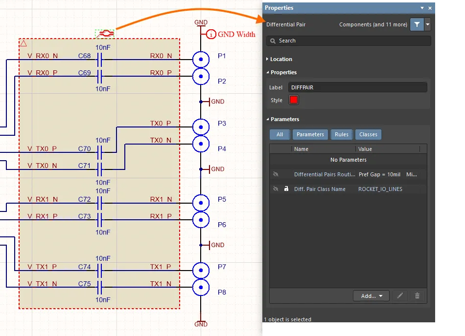
The Differential Pair directive is used to define a net class and a design rule, which is then applied to targeted diff pairs.
Working with Differential Pairs
The Differential Pair directive is used to indicate nets that belong to a differential pair. The software requires the nets in the pair to be named <Name>_P and <Name>_N. The PCB differential pair will then be named <Name>.
Pairs can be defined by placing a Differential Pair directive on every differential pair member, or a blanket can be placed so that it covers the pair net names, as shown in the image above.
Referring to the image above, the differential pair Parameter Set object results in the creation of:
-
Eight differential pairs, named
V_RX0, V_TX0, V_RX1, V_TX1, RX0, TX0, RX1, TX1.
-
A PCB net class, called
ROCKET_IO_LINES.
-
A
Differential Pairs Routing design rule, configured to target the PCB Net Class, ROCKET_IO_LINES.
Configuring the ECO Generation Options
The Options for Project dialog also includes an ECO Generation tab. This tab defines which design modifications can have ECOs created. Typically these are all enabled, with the options in the Comparator tab of the dialog being used to configure which design changes are to be synchronized between the schematic and the PCB.
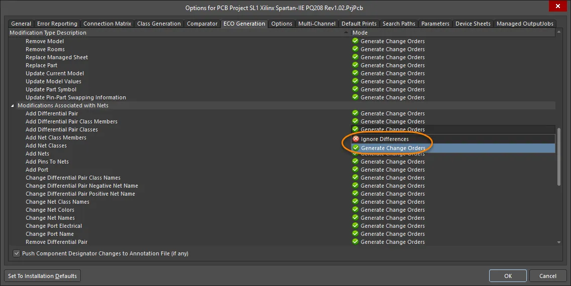
The ECO Generation tab defines which types of modifications can have ECOs created.
Finding Differences
The design synchronization feature is able to detect and resolve differences in both directions; that is, from the schematic to the PCB, or from the PCB back to the schematic.
There are two approaches to detecting and resolving differences:
-
Assign the update direction for each change.
-
Apply all updates in the same direction.
If you do not need to apply updates in both directions at the same time, then you do not need to go through the process of choosing the documents to compare and configuring the update direction for resolving the differences. In this case, you can go straight to the Performing a Direct Update section.
The software is capable of resolving these differences by applying changes to both sides, at the same time. For example, imagine the scenario where the electronics designer has changed the value of a capacitor, while the PCB designer has changed the footprint of that same capacitor. These two differences can be resolved in a single update process, by applying the comment change as a schematic-to-PCB update, and the footprint change as a PCB-to-schematic update.
When the comparator engine compares the schematic project to the PCB, a complete list of differences is created - at this stage there is no assumption on which side must be changed to bring them back into sync.
The list of differences can be seen in the Differences between dialog.

Options and Controls of the Differences between Dialog
The dialog is essentially divided into three main regions - Differences, Update and Change Order.
Differences
This region of the dialog lists all differences that the Comparator has found between the chosen documents. Each difference is listed in the corresponding column for the document in which it resides. Differences are grouped by comparison type as listed and enabled on the Comparator tab of the Project Options dialog. The entry at this group level reflects the number of differences of that type.
Double-click on an entry to cross probe to the object on the relevant source document.
Use the Expand All and Contract All commands on the right-click menu to quickly expand or contract all entries. You also can expand or contract individual comparison type groupings using the +/- controls to the left of each entry.
When comparing the design hierarchy of a project to its PCB document, the column for the project side will be labeled with the name of the top-level schematic sheet.
Update
Use this region of the dialog to specify which document should be updated in order to remedy the difference. By default, all Decision entries initially have a decision of No Change applied to them.
Even if differences are detected, you are under no obligation to take action on them. The software will only synchronize the elements you specify.
The update decision for each difference can be individually determined by clicking on the associated entry in the Decision column then selecting the required update action in the subsequent ![]() ECO Decision dialog. Simply choose the direction of the update (which of the compared documents to update) or No Updates at all.
ECO Decision dialog. Simply choose the direction of the update (which of the compared documents to update) or No Updates at all.
The ECO Decision dialog provides an indication of whether or not the update in a particular direction is valid. If valid, the corresponding arrows are enabled. If a change is not supported, the corresponding button for that update direction is grayed out.
Change Order
This region of the dialog lists (for each difference that you decide to act upon) the action to be taken, the object affected by the action, and the document upon which the action will be carried out. It is this information that is used to compile the subsequent ECO that will be used to create the updates. Common actions that will be listed in this area are:
-
Remove - where the update is in the direction of the document that contains the object causing the difference; the object will be removed.
-
Add - where the update is in the direction of the document that does not contain the object causing the difference; the object will be added.
-
Update - where both documents contain the same object that differs in some way; the object changed depends on the direction chosen.
If the Update Decision is No Change, there will be no action taken as reflected in the Change Order entry No Action.
Right-click Menu
-
Create Change Order - use to create an Engineering Change Order (ECO).
-
Generate Report - use to generate a report for the differences found by the Comparator. The update decisions you have decided to make and the actions will be included in the generated ECO. The report will be loaded into the Report Preview dialog. Use this dialog to browse the report, before ultimately exporting it to one of various supported formats or printing it directly.
-
<< Update All in - use to set the update direction for all differences to the left-hand document (where applicable).
-
Update All in >> - use to set the update direction for all differences to the right-hand document (where applicable).
-
Reverse Direction For All - use to quickly reverse the update direction for all differences (where applicable). If it is not valid to change the direction for a difference, the entry will be set to No Change.
-
Set No Action For All - use to quickly set the update decision for all differences to No Change.
-
<< Update Same Kind in - use to set the update direction for all differences of the same comparison type as the currently focused difference to the left-hand document (where applicable).
-
Update Same Kind in >> - use to set the update direction for all differences of the same comparison type as the currently focused difference to the right-hand document (where applicable).
-
Reverse Direction For Same Kind - use to quickly reverse the update direction for all differences of the same comparison type as the currently focused difference, where applicable. If it is not valid to change the direction for a difference, the entry will be set to No Change.
-
Set No Action For Same Kind - use to quickly set the update direction for all differences of the same comparison type as the currently focused difference to No Change.
-
<< Update Selected in - use to set the update direction for all selected differences to the left-hand document (where applicable).
-
Update Selected in >> - use to set the update direction for all selected differences to the right-hand document (where applicable).
-
Reverse Direction For Selected - use to quickly reverse the update direction for all selected differences (where applicable). If it is not valid to change the direction for a difference, the entry will be set to No Change.
-
Set No Action For Selected - use to quickly set the update decision for all selected differences to No Change.
-
Invert Selection - use to select all differences not currently selected in the list or deselect those that are.
Multiple differences can be selected in the list using standard multi-select techniques (Ctrl+click, Shift+click).
An update in a particular direction will only be set if it is valid to do so.
Additional Controls
The following buttons are available at the bottom of the dialog:
-
Create Engineering Change Order - click this button to generate an ECO. The Engineering Change Order dialog will appear from where you can validate and execute the updates in order to synchronize the documents.
-
Report Differences - click this button to generate a report for the differences found by the Comparator. The update decisions you have decided to make and the actions will be included in the generated ECO. The report will be loaded into the Report Preview dialog. Use this dialog to browse the report before ultimately exporting it to one of various supported formats or printing it directly.
-
Explore Differences - click this button to investigate further the differences found by the Comparator prior to generating an ECO. The Differences between dialog will close and you will be returned to the main workspace with the Differences panel open. The panel will contain all of the differences listed by the Comparator and in the same categories. Use the panel to cross probe to an object responsible for a difference on its parent document.
Exploring differences in this way will cause any update decisions you have made in the Differences between dialog to be lost. You will need to open the dialog again and redefine updates as required. Alternatively, you can cross probe to an object directly from within the Differences between dialog. Double-click the object's entry in the Differences region of the dialog. Since the Differences between dialog remains open, it is a good idea to have the source and target documents open and the dialog placed so that your view is not obscured.
To open the Difference between dialog and see a list of differences:
-
To open the Choose Documents to Compare dialog, as shown in the image below, run the Project » Show Differences command or right-click on the entry for the required project (or one of its source documents) in the Projects panel and choose the Show Differences command, from the context menu. The Choose Documents to Compare dialog is used to select what two documents/document-sets you will be comparing, typically it is the schematic project against the PCB. You can also use this dialog to compare any document to any document by ticking the Advanced Mode option. For example, you might be comparing a netlist to a PCB, or a PCB to a PCB.
Generally, the default setup of the dialog - in either basic or advanced modes - is fine for most design comparison needs, where the source documents and target PCB design are needed to be compared with a view to achieving synchronicity. The dialog will allow you to compare other documents though and this can be useful if you need to load versions of a project and compare the differences between corresponding source documents.
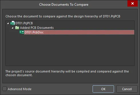
Select the PCB to compare the schematic project against.
-
Select the PCB in the main part of the dialog, and click OK to open the Difference between dialog, as shown below. If the PCB document is currently synchronized with the source documents, a dialog will appear stating that no differences were detected.
The Differences between dialog will open. The Synchronizer is bi-directional. This means you can specify updates to both documents in the same ECO. In order to synchronize compared documents, the aim is to determine, for each difference, whether or not to take action and in which direction the change is made - specifying which document should be updated in order to remedy the difference. The next step is therefore to assign an update direction to each difference:
-
For an individual difference, click in the Update column to display a direction selector, as shown in the image below.
-
For multiple differences of the same kind, right-click on a heading, such as Different Footprints, and select the required Update Same Kind command.
-
For all differences, right-click anywhere in the dialog and select the required Update All command.

For each difference, the Update direction must be set for an ECO to be created to resolve that difference.
Click the Explore Differences button to access the Differences panel and explore the differences as described in the Exploring Design Changes with the Differences Panel section below.
Since accessing the Differences panel in this way closes the Differences between dialog, any update decisions already made will be lost. It is therefore better to explore differences before making update decisions. Alternatively, cross probe to an object directly from within the Differences between dialog, by double-clicking the object's entry in the Differences region of the dialog.
Click Report Differences to set up and print/export a report for the differences found by the Comparator, the update decisions specified and the actions that will be included in the generated ECO.
Once the Update direction has been assigned, click the Create Engineering Change Order button to open the Engineering Change Order dialog, which is described in the Resolving Differences - Applying the ECOs section below.
Exploring Design Changes with the Differences Panel
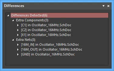
The Differences panel displays a hierarchical view of document differences.
Summary
The Differences panel is used to display the logical or physical differences found by the software's built-in Differences Comparator when comparing design documents (for example, when comparing the source document hierarchy (schematics) for a project against the PCB design document). The panel allows you to interactively explore the differences before the decision to create an Engineering Change Order (ECO) that will be used to synchronize the project documents.
Panel Access
To open the Differences panel:
-
Choose View » Panels » Differences from the main menus.
-
Click the Panels button on the bottom right-hand side of the design workspace, then click Differences.
Panels can be configured to be floating in the editor space or docked to sides of the screen. If the Differences panel is currently in the group of docked panels, use the Differences tab located at the bottom of the panels to bring it to the front.
Displaying Differences
How the Differences panel is applied depends on whether the goal is to:
-
Analyze the integrity of the complete project in terms of its content and structure by detecting logical differences within the project hierarchy.
-
Compare two versions of the same Schematic or PCB document by detecting their graphical (physical) differences.
The
Differences panel is populated when using the
Explore Differences feature of the Differences Comparator
Differences between dialog, which is opened by right-clicking in the
Projects panel then choosing
Show Differences.
Displaying Logical Differences
Comparison of project documents for logical differences is done in the Choose Documents To Compare dialog, activated by right-clicking on a project (or project document) in the Projects panel then selecting Show Differences from the associated context menu.

Right-click on a project name then select Show Differences to open the Choose Documents To Compare dialog.
Typically, the PCB document would be compared against the source document hierarchy for the parent project to detect logical differences between the schematic design content and the PCB design content.
After clicking OK, if any differences exist between the nominated documents, the Differences between dialog will open. Information in the Differences panel will only appear after clicking the Explore Differences button in the Differences between dialog.
The Differences panel will display only the differences that are listed in the Differences between dialog. These, in turn, are determined by the selections made in the Comparator tab of the Project Options dialog (Project » Options). This tab lists all of the comparison types, such as differences associated with Components, Nets and Parameters. Setting the Mode for each comparison category between Find Differences or Ignore Differences will determine if the Differences Comparator passes its results into the Differences between dialog.

Set up how the differences are detected and reported in the Project Options dialog.
The Differences panel displays the differences found between source documents in a tree-like structure, where the top-level folder displays the total number of differences detected. Sub-folders are then created for each specific comparison type that appears in the Differences between dialog. Each sub-folder lists the specific differences that have been found, which, in turn, are broken down further into objects on the documents that are responsible for creating those differences.
If the associated document is open (or open and hidden), clicking on an object entry in the panel will cross-probe to the object on the document.
The visual display of the object uses the zoom and dim effect where the object is highlighted by dimming all other objects. The contrast of the dimming can be varied with the Dimming slider found in the Highlight Methods region of the System - Navigation page of the Preferences dialog.
Displaying Physical Differences
The graphical (physical) comparison of two versions of the same schematic or PCB document is carried out basically in the same way as the logical comparison outlined above, but also makes use of the Advanced Mode in the Choose Documents To Compare dialog.
Perform a document physical comparison using the Show Differences command (Projects panel right-click menu) to open the Choose Documents To Compare dialog then check the Advanced Mode box. With all project files now shown in the dialog, select the two variations of a document for comparison.
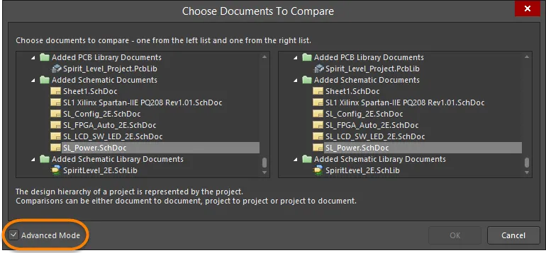
Selecting documents for physical comparison from the Choose Documents To Compare dialog in Advanced Mode.
Clicking OK will proceed with the graphical comparison and open the Differences between dialog as outlined previously. Click Explore Differences to open the interactive differences list in the Differences panel.
The panel displays the differences found between the documents in a tree-like structure. The top-level folder displays the total number of differences detected. Entries are created for each type of difference, which, in turn, contains the specific references and the object (port, part, etc.,) involved for each.
Selecting the object entry for a detected difference will highlight and zoom to the object in the editor design space.
Notes
-
If an object in the panel resides on a document that is currently hidden, the document will be opened automatically and made the active document in the design editor window when you click the associated entry.
-
The filtering applied when cross-probing from the Differences panel is temporary. As such, you are not prevented from selecting or editing design objects that fall outside the scope of the filter.
-
The information in the Differences panel will be cleared when performing a new document comparison or compiling the parent project.
-
Use the Project » Show Physical Differences command from the main menus to detect the physical differences that exist between two versions of a schematic or PCB document, and present these differences graphically when viewing the two documents side-by-side in the design space. This Show Physical Differences feature offers purely visual comparison – neither of the documents being compared can be updated by generation of ECOs. It is intended for comparison of two versions of the same document, but if run to compare different documents, such as the project’s source hierarchy with the PCB, the Differences panel will appear listing the detected logical differences.
Performing a Direct Update
Since the designer usually knows which way they want to apply the updates and those updates are all in the same direction, you can choose to skip the difference detection and direction assignment process that has just been described.
Rather than selecting the Show Differences command from the Project menu, you choose the Update command from the Design menu, from either the schematic editor or the PCB editor. Your choice of editor from which you run the command, indicates the direction you want the changes to be made - from this editor, to that editor. For example, you would choose Design » Update in the schematic editor to push all changes from the schematic to the PCB.
The active PCB design document can also be with any changes that have been made to the source schematic documents by choosing the Design » Import Changes from <ProjectName> command, from the main menus of the PCB editor.
The Differences between dialog will be skipped and you will jump straight to the Engineering Change Order dialog.
 If all of the updates are going to be applied in the same direction, use the Design » Update command.
If the PCB document is currently synchronized with the source documents, a dialog will appear stating that no differences were detected. Conversely, when updating schematics, it is also possible that some, or none of the detected differences, can be resolved by automatically generated ECOs. In this case, you will be given the option to view these differences, through the
Differences between dialog. While a modification may not be possible in the direction of the schematics, it may be that you need to update the PCB (perhaps by removing an object or entity). After sifting through the differences, if you are able to resolve some, or all of them, you can generate an ECO. If there remain differences that can't be resolved through the dialog, you will need to return to the design to resolve the issues, before running a comparison again.
Resolving Differences - Applying the ECOs
Each difference is resolved by applying an Engineering Change Order (ECO). The ECOs are listed in the Engineering Change Order dialog with one ECO per line, each with its own Enable checkbox.
When using the Engineering Change Order dialog:
-
The dialog opens with all changes enabled, disable any changes you wish to hold off for now. The dialog supports multi-select - use the right-click context menu to toggle the enable state of selected ECOs.
-
Use the right-click Cross Probe command to examine the objects affected by that ECO.
-
Use the Validate Changes button to check that the changes can be performed. ECOs typically fail because an object is not available - for example, the specified PCB footprint does not exist in the Available File-based Libraries, or the specified pad does not exist on the footprint.
-
An ECO can also fail because an object that is needed by a certain ECO was not present, but was added during the processing of the current ECOs. In this situation, run the Update command again to complete that ECO.
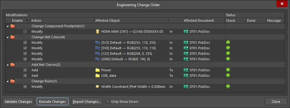
Each design change presents as an ECO, enable those that are required.
Options and Controls of the Engineering Change Order Dialog
The dialog is divided into two main regions: Modifications and Status.
Modifications
This region of the dialog lists all modifications necessary to implement the changes required to bring about synchronization. Modifications are grouped by modification type as listed and enabled on the Project Options - ECO Generation dialog. The entry at this group level reflects the number of modifications of that type. Each specific modification in this region is listed in terms of the following:
-
Enable - this option determines whether or not the modification will be included when the ECO is executed. Click directly on the checkbox to toggle its state between enabled/included (checked) and disabled/excluded (unchecked). You can toggle the Enable check box on and off by using the spacebar.
-
Action - the specific action to be carried out. The types of actions are dependent on what type of ECO needs to be done.
-
Affected Object - the object affected by the action.
-
Affected Document - the document upon which the action will be carried out.
Multiple modifications can be selected in the list using standard multi-select techniques (Ctrl+click, Shift+click).
If the
Mode for a modification type has been set to
Ignore Differences on the
ECO Generation tab of the
Project Options dialog, any design update that results in the action of this modification type will not be transferred to the
Engineering Change Order dialog.
Right-Click Menu
By default, all modifications are enabled for inclusion when the ECO is executed. Enable/disable each modification entry as required, either individually or use the following commands available from the right-click menu to change the enabled state of multiple modifications:
-
Validate Changes - click to run a validation check on the modifications enabled for inclusion in the ECO. Validation results will appear in the Check column under the Status region of the dialog.
-
Execute Changes - click to execute the ECO. Execution results will appear in the Done column under the Status region of the dialog. Remember, only changes that pass the validation stage will be executed.
-
Create Report - click to generate a report for the modifications contained in the ECO. The report will be loaded into the Report Preview dialog.
-
Cross Probe - click to cross-probe to target and reference objects that are involved in a modification action on the associated schematic and PCB documents.
-
Expand All - click to expand the view of all modifications in the listing.
-
Contract All - click to contract the view of all modifications in the listing.
You can also expand or contract individual modification groupings using the +/- controls to the left of the entry.
-
Enable All - use to enable all modifications.
-
Disable All - use to disable all modifications.
-
Enable Selected - use to enable all selected modifications.
-
Disable Selected - use to disable all selected modifications.
-
Enable all of same Kind - use to enable all modifications of the same modification type as the currently focused modification.
-
Disable all of same Kind - use to disable all modifications of the same modification type as the currently focused modification.
-
Invert Selection - use to quickly select all modifications not currently selected in the list and deselect those that are.
Status
This region of the dialog presents the following status information for each enabled modification:
-
Check - this field shows the result of running a validation check on the modification. A green check (
 ) means that the proposed change is supported and will be carried out upon execution of the ECO. A red cross (
 ) means that the proposed change is invalid and will not be carried out when the ECO is executed.
-
Done - this field shows the result of the execution of the modification. A green check (
 ) means that the valid modification executed successfully.
-
Message - if the modification fails the validation stage, an entry will appear in this field (and also in the Messages panel), giving an indication as to why it failed.
You can close out of the dialog at any stage in order to investigate why certain changes are failing and make any design changes necessary.
Additional Controls
The following controls are available at the bottom of the dialog and in the right-click menu:
-
Validate Changes - click to run a validation check on the modifications enabled for inclusion in the ECO. Validation results will appear in the Check column in the Status region of the dialog.
It is important to validate the proposed modification actions before executing them. This tests the logic of your proposed changes.
-
Execute Changes - click to execute the ECO and effect the valid changes contained therein. Execution results will appear in the Done column in the Status region of the dialog. Remember that only changes that pass the validation stage will be executed.
-
Report Changes - click to generate a report for the modifications contained in the ECO. The report will be loaded into the Report Preview dialog.
Keep in mind that the report will list all modification entries regardless of whether they validate and execute successfully.
-
Only Show Errors - check this option to only show Engineering Change Order errors. Validated changes will not be displayed. Showing only the list of errors will enable you to quickly review and make necessary changes to your design so that the resulting ECO validates completely.
Comparator-related messages will be displayed in the Messages panel.
Understanding the Linking Between the Schematic and the PCB
Component Matching via Unique Identifiers
Each schematic component links to its PCB component through a Unique Identifier (UID). The UID is assigned when the schematic component is placed on the sheet, and this value is transferred to the PCB component when the design is transferred to the PCB editor. When component information is transferred for the first time between schematic source documents and the blank PCB design document, using the Synchronizer, all components will automatically be linked by unique ID – the ID information from each schematic component being assigned to the corresponding component footprint.
This scheme would be adequate for a simple design, but is not capable of supporting a multi-channel design. In a multi-channel design, the same schematic component is repeated in each physical channel, which would mean the repeated PCB components would have the same UID. To cater for this, the UID for the PCB component is created by combining the UID of the parent Sheet Symbol with the UID of the schematic component. The syntax of the PCB UID changes slightly, depending on how the multi-channel design has been created.
For a multi-channel design created by placing multiple Sheet Symbols that all reference the same schematic sheet, then each Sheet Symbol can provide a unique ID, so the PCB UID has the format:
\SheetSymbolUID\SchComponentUID
For a multi-channel design created using the Repeat keyword, there is only 1 Sheet Symbol UID available, so the PCB UID also includes the ChannelIndex value, in the format:
\ChannelIndex+SheetSymbolUID\SchComponentUID
The UIDs are not displayed in panels and dialogs.
When the Components are not Linked
The advantage of using a UID to match the schematic and PCB components is that it allows the designators to become unsynchronized (perhaps by performing a PCB re-annotate a number of times), without any risk of the schematic and PCB becoming unsynchronizable.
If there is a component present on the schematic or the PCB that does not have a matching component (same UID) present in the other editor, the following will occur:
-
If the extra component is only present in the source editor, an ECO to add the component to the target editor will be generated.
-
If the extra component is only present in the target editor, an ECO to remove the extra component will be generated.
-
When there are unmatched components present in both editors, the software needs instruction on how to deal with them, so the Failed to Match Unique Identifiers dialog opens.
 The Failed to Match Unique Identifiers dialog
The dialog buttons have the following options:
-
Automatically Create Component Links - click this button if you know that the unmatched components already have matching designators. Using the component designators, the software will assign matching UIDs to these extra components. For components that can be matched by designator, any other property differences (such as unmatched parameters), will result in ECOs being generated. If there are components that cannot be matched by designator, ECOs to add/remove these will be generated (extra components present in the source editor to be added, extra components in the target editor to be removed).
-
Manual Component Links - click this button if you know there are components that match, but do not know the status of their designators. The Edit Component Links dialog will open (described below), where you can manually select each source and target component and transfer them to the matched components list, assigning them matching UIDs. ECOs will then be generated to synchronize the designators (and any other unmatched component properties).
It is a good idea to have all components matched using unique IDs so that annotation of designators in either the schematic or PCB document can be carried out with the knowledge that the documents can still be re-synchronized at any stage. The documents can still be synchronized even if components aren't matched by unique IDs, but in this case, you will be prompted to match the components by designators only - comment and footprint are not taken into account, and therefore it is possible that matching of some components is carried out incorrectly.
-
Cancel - click this button to generate ECOs to add extra components that are present in the source editor and remove extra components from the target editor.
Manually Linking Components
The status of the component links between schematic components and their corresponding PCB component footprints can be checked and managed at any time, in the Edit Component Links dialog (PCB editor, Projects » Component Links command).
The reason that manual linking of components is only carried out from within the PCB document, is that only the PCB component footprints need to be updated with the unique ID information - it is already present on the schematic side.
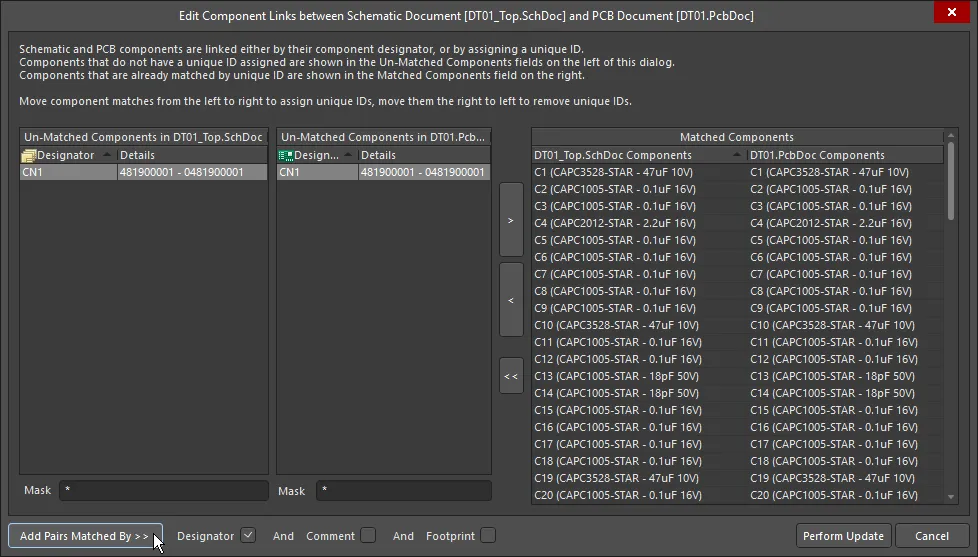
The Edit Component Links dialog is used to detect and resolve UID mismatches, it is run from the PCB editor.
Summarizing the dialog features:
-
Components that are unmatched are presented in the two Un-Matched Components columns on the left, components that share a matching UID are presented in the Matched Components region on the right of the dialog.
-
The arrow buttons in the middle of the dialog are used to manually match (or un-match) selected components, or unmatch all currently matched components.
-
The Add Pairs Matched By button and options down the bottom of the dialog are used to scan the list of currently unmatched components, and attempt to match them by the enabled properties (Designator, Comment, Footprint).
-
When the Perform Update button is clicked, each newly matched PCB component is assigned the UID of its schematic counterpart. If you have moved any entries in the Matched section of the dialog back into the Unmatched sections, a confirmation dialog will appear advising that existing component associations will be broken by proceeding. Clicking Yes will proceed with the update and an information dialog will appear giving a summary of the component links modified in the PCB document. A new entry in the Matched section is summarized as a Link Modified, whilst a previously linked entry that you have now unmatched is summarized as a Link Removed.
-
After using this dialog to perform manual component linking, it is good practice to check the synchronization state (run the Design » Update command).
-
Use the dialog at any stage during the design, to view the linking between components and to reassure yourself that the components on the schematic source documents are indeed correctly matched to the corresponding component footprints in the PCB design.
-
Unique IDs can be removed at any time by moving the linked components back to the unmatched regions of the Edit Component Links dialog. Removing a component link will remove the unique ID from the corresponding PCB footprint only. The schematic component retains the unique ID, unless a new one is generated (using a reset unique ID-related command at the schematic level).
-
A unique ID is also automatically assigned to each parameter definition on a source schematic document. This is used for those parameters that have been added as design rule directives. When transferring the design to the PCB document, any defined rule parameters will be used to generate the relevant design rules in the PCB. These generated rules will be given the same unique IDs, allowing rule constraints to be changed in either schematic or PCB and those changes pushed across when performing a synchronization.
-
If you copy/paste or cut/paste a schematic component, its UID is automatically renewed - this ensures that every component continues to have a unique identifier.
-
If you are reorganizing your schematic (which has already been transferred to the PCB editor) and need to move components to another sheet, don't cut/paste them, select them and run the Edit » Refactor » Move Selected Sub-circuit to Different Sheet command.
Matching the Nets and Classes
Both nets and classes have a parent (the net or class), and children (the members of that net or class). Matching these requires a different approach than the UID mechanism used for component linking, to support changes to: the parent; the children; or both the parent and its children. For example, something as simple as changing the name of a net on the schematic should not require that net and all its children pins be removed from the PCB, then the newly named net be added, and finally all the children pins be added to that new net.
To support this, the software includes separate matching algorithms to match nets and classes by their members, and also by their name. The matching process is configured in the Object Matching Criteria section of the Comparator tab of the Options for Project dialog.

The default settings is to match members first, then by Object Type name.
Matching for these types of objects is handled in the following way:
-
During design synchronization, the default behavior is to first attempt to match by members, in accordance with the Min Match % and Min Match Member settings.
-
If member matching fails, the software will then attempt to match by name (if the Use Name Matching option is enabled).
-
If either of these matching processes succeeds, you will proceed to the Engineering Change Order dialog.
-
If both matching techniques fail (or the Use Name Matching option is set to
Never), the Match Manually dialog will open.

-
Clicking No in the Match Manually dialog will skip the user-matching process and jump straight to the Engineering Change Order dialog. Since you have not attempted to match any unmatched objects, the software assumes that the reference and target objects are unrelated, so ECOs will be generated that remove the Unmatched Reference Objects from the board, and add the Unmatched Target Objects as new objects.
-
If you click Yes in the dialog to match manually, the Match dialog will open, as shown below (the dialog caption will change to suit the unmatched object type).
 The Match dialog is used to manually match objects that you know to be matched. Leave the right side empty and click Continue if you are unsure.
Options and Controls of the Match Dialog
-
Unmatched <Object>
-
Unmatched Reference Objects - lists the unmatched objects. Use the expand/collapse controls to open/close the list.
-
Unmatched Target Objects - lists the target objects. Use the expand/collapse controls to open/close the list.
-
 - click to match the selected reference and target objects and move the selected object(s) from the Unmatched region to the Matched Pairs region.
-
 - click to move the selected object(s) from the Matched Pairs region to the Unmatched region. This action will cause the moved objects to be unmatched.
-
 - click to move all objects from the Matched Pairs region to the Unmatched region. This action will cause the moved objects to be unmatched.
-
Matched Pairs - lists the Reference Object and Target Object that are now matched.
-
Continue - click to accept the matching updates and open the Engineering Change Order dialog.
-
In this dialog, select the objects that you want matched in the Unmatched Reference Objects and Unmatched Target Objects, and then transfer them to the Matched Pairs section of the dialog. For these objects, the software will generate an ECO to update the names so they now match, and ECOs to remove/add members, so they also match.
-
If you are unsure, you do not have to manually match objects. For any unmatched objects, the software assumes that the reference and target objects are unrelated, so will generate ECOs that remove the Unmatched Reference Objects from the board, and add the Unmatched Target Objects as new objects.
-
Once you have matched those objects that you know do match, click Continue to open the Engineering Change Order dialog.
-
If you click Cancel, the update process terminates.
Matching the Design Rules
Design rules that are defined on the schematic must also be linked to the matching rule on the PCB. If there was no linking mechanism, you would not be able to update the rule on the schematic and flow those changes to the PCB. UIDs are used to link the schematic design rule to the PCB design rule.
The UID is automatically assigned in the Parameter Set that holds the rule definition on the schematic, and transferred to the PCB during design design synchronization.
 Design rules use a UID to match the schematic design rule definition to the PCB design rule.
Typically, you will not need to manually manage the matching of rules, unless you have manually edited the UID in the PCB Rules and Constraints dialog in the PCB editor. If the UIDs do not match, the software will add a new rule to the PCB for any schematic rule that does not have a matching PCB rule, and remove any PCB design rule that does not have a matching schematic design rule.
You can freely update components in either editor and synchronize those changes to the other editor. Changes made to nets, classes, and rules can only be updated from the schematic to the PCB.