Saving an Altium Designer Document to a Previous File Format
An Altium Designer schematic, schematic library, PCB or PCB library file can be saved to a previous Protel/Altium file format. In an Outputjob file, click [Add New Export Output] and select an entry in the Save As/Export PCB or Save As/Export Schematic menu, then double-click the added output to access the Save As / Export Output Setup dialog and choose the required format. The export outputs can then be generated directly from the file or as part of the Project Release process.
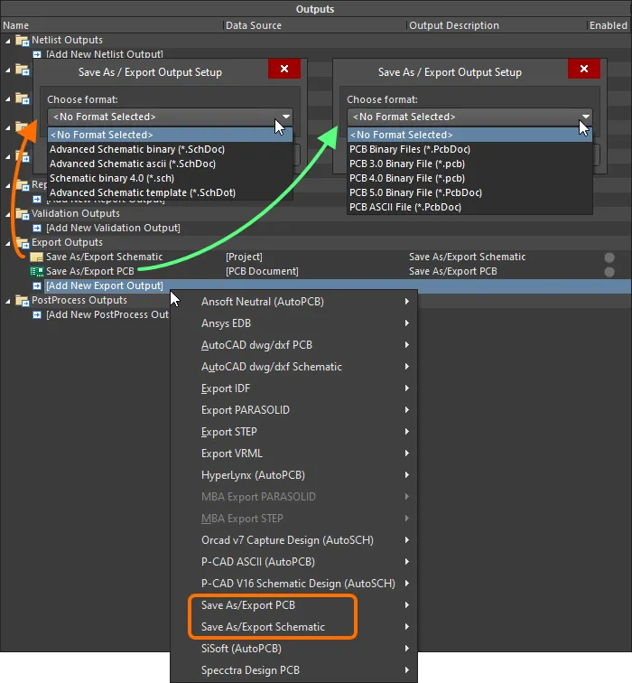
Alternatively, use the File » Save As command (or the File » Save Copy As command) from the main menu of an appropriate editor and then select the required file format from the Save as type drop-down of the Save As dialog that opens.
CircuitStudio, CircuitMaker, PCBWorks Import-Export Support
Importing and Exporting CircuitMaker (current version), CircuitStudio and PCBWorks PCB Files
Altium Designer includes the capability to import PCB files of other Altium formats and export a PCB to CircuitMaker, CircuitStudio and PCBWorks format files.
To import a CircuitMaker (*.CMPcbDoc), CircuitStudio (*.CSPcbDoc) or SolidWorks (*.PWPcbDoc, *.SWPcbDoc) PCB file to the active Altium Designer PCB document, select the File » Import » Altium PCB command from the main menus of Altium Designer's PCB editor.
An active Altium Designer PCB document can be exported to the CircuitMaker (*.CMPcbDoc) and CircuitStudio (*.CSPcbDoc) file format. To do this, select the File » Export » CircuitMaker or File » Export » CircuitStudio command from the main menus of Altium Designer's PCB editor.
Importing CircuitMaker 2000 Schematic and Library Files
Altium Designer includes the capability to import CircuitMaker 2000 files through the Import Wizard. The Wizard is a quick and simple way to convert CircuitMaker design files to Altium Designer files. The Wizard walks you through the import process and handles both the schematic and library files.
The CircuitMaker 2000 schematic and library file importer is available through Altium Designer's Import Wizard (File » Import Wizard) by selecting the CircuitMaker 2000 Schematics and Libraries Files option on the Wizard's Select Type of Files to Import page.
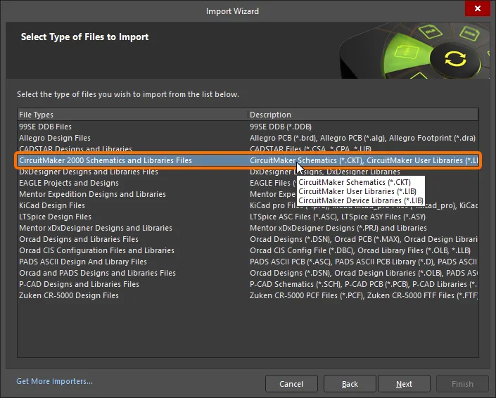
Select CircuitMaker 2000 Schematics and Libraries Files in the Import Wizard to import CircuitMaker 2000 files.
The Import Wizard will guide you through the steps involved when importing these types of files including:
- CircuitMaker Schematics (*.CKT).
- CircuitMaker User Libraries (*.LIB).
- CircuitMaker Device Libraries (*.LIB).
Import Wizard - CircuitMaker 2000 Schematics and Libraries Files
CircuitMaker 2000 Schematics and Libraries Files
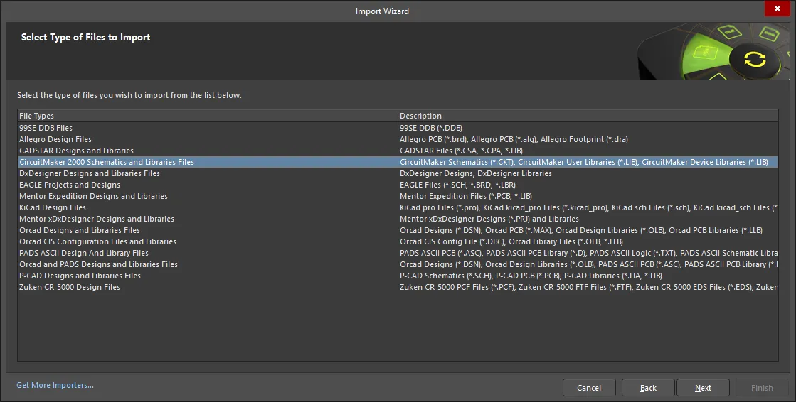
Importing CM2000 Design Files
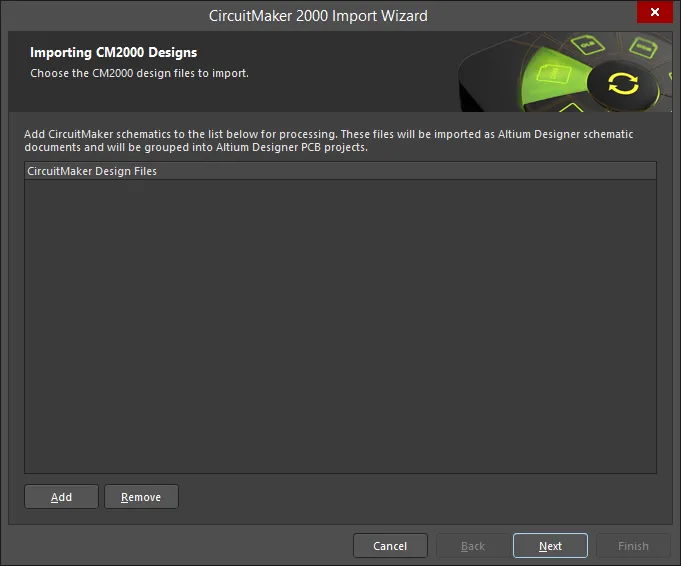
Click Add to choose which CircuitMaker schematic files to import. The added files will be imported as Altium Designer schematic documents and will be grouped into Altium Designer PCB projects. You can delete a selected file by clicking Remove.
Selecting CM2000 Library Files
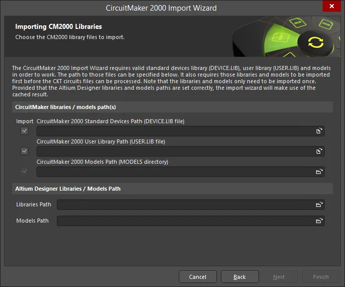
The Wizard requires valid standard devices library files (DEVICE.LIB), user library files (USER.LIB), and models. The Wizard also requires those libraries and models to be imported first before the .CKT files can be processed. The libraries and models need to be imported only once. If the Altium Designer libraries and models paths are set correctly on this page of the Wizard, the import process will make use of the cached result.
-
CircuitMaker libraries / models path(s)
Use the Browse folder icons to set the desired paths for CircuitMaker 2000 Standard Devices Path (DEVICE.LIB file), CircuitMaker 2000 User Library Path (USER.LIB file), and CircuitMaker 2000 Models Path (MODELS directory).
Enable Import for each library and/or model path you want to import.
-
Altium Designer Libraries / Models Path
Use the Browse folder icons to set the Libraries Path and Models Path.
Setting Reporting Options
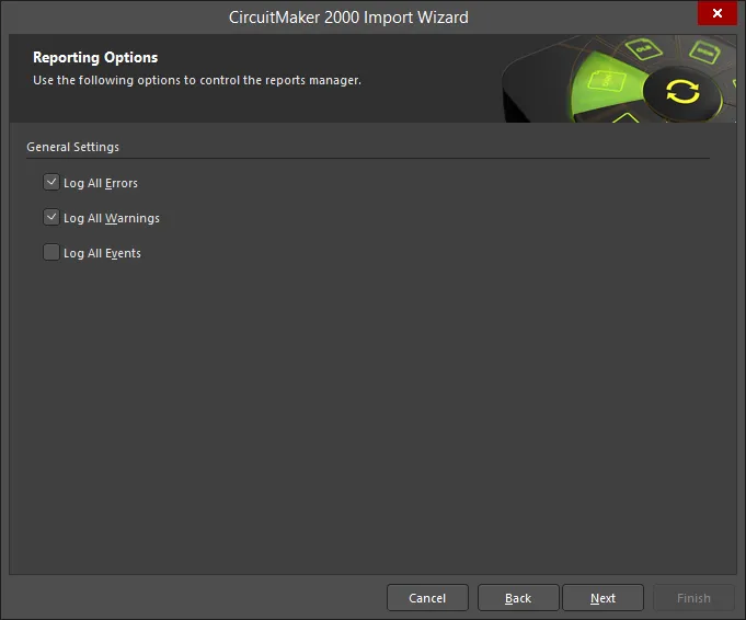
Use the Reporting Options page to set up general log reporting options.
Under General Settings, enable the desired options: Log All Errors, Log All Warnings, Log All Events.
Specifying the Output Directory
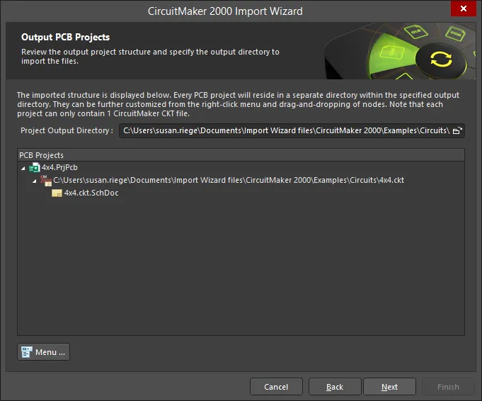
Every PCB project will reside in a separate directory within a specified output directory. Note that each project can contain only one CircuitMaker .CKT file. Use this page of the Wizard to review the output project structure and specify the output directory in which to import the files. Use the Browse Folder icon to search for and choose the Project Output Directory.
Click Menu to access options to edit the project structure:
Right-clicking in the PCB Projects region gives access to the same menus and sub-menus as clicking the Menu button.
A page opens and displays the document that is currently being processed with a green bar to show the progress of the import.
Closing the Wizard
The CircuitMaker 2000 Import Wizard has completed. Click Finish to close the Wizard.
Imported CircuitMaker 2000 files translate as follows:
- CircuitMaker 2000 schematics (
*.CKT) translate to Altium Designer schematic documents (*.SchDoc).
- CircuitMaker 2000 user and device libraries (
*.LIB) translate to Altium Designer schematic libraries (*.SchLib).
Protel Design Files Import-Export Support
Importing a Protel 99 SE Database
Protel 99 SE uses the design database, or DDB, to store design files. The 99SE Import Wizard gives control and visibility over the process of importing a 99SE design database into Altium Designer.
Design Database Becomes a Project Group & Projects
Protel 99 SE stores all design documents inside a single design database. The database acts as a storage container, and also as a way that the designer can group project-related design files.
There is no hard and fast requirement on what is stored in a design database, or how the design documents might be grouped into folders within the design database (DDB). Some designers use a single DDB for each board design, others keep all revisions of a design in a single DDB, while other designers keep all board designs for one product in a single DDB.
In Altium Designer, all design files are stored on the hard drive. The basis of every design created in Altium Designer is a project file. Multiple types of projects are supported in the environment, including PCB projects (*.PrjPcb). Apart from script projects, a fundamental requirement is that each project targets a single implementation - for example, a PCB project includes all the sources required to define a single PCB. The project file itself is an ASCII file that stores project information, such as links to the documents that are in the project, output settings, error checking settings, and so on.
Above the project level, Altium Designer uses the project group. A project group (*.DsnWrk) is used to cluster related projects together, so you could use a project group for all projects for one customer, all boards in one product, and so on. When you open a project group, all projects that are in that group will appear in the Projects panel.
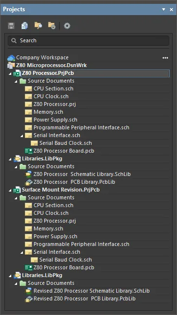
The image below shows the default mapping from a 99 SE design database to the equivalent objects in Altium Designer; a project group is created for the DDB, a PCB project for each folder that includes a PCB file, and a Library Package for each folder that only includes libraries. During import, you have the opportunity to change all of the mappings, except the DDB to project group.
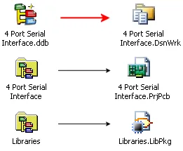
While Altium Designer allows direct editing of any individual schematic, PCB, or any other design file, to perform any project-type operations, such as updating the board from the schematic or printing all the schematics in the project, you must open the project.
Protel 99 SE Windows File System designs can also be imported. Use the 99 SE Import Wizard in the same way as you would with an Access® Database DDB.
If you are interested in walking through the entire PCB design process in Altium Designer using a simple example, see Tutorial - A Complete Design Walkthrough with Altium Designer.
Importing the Database
To import a 99 SE database, select File » Import Wizard. On the Select Type of Files to Import page of the Import Wizard, select 99SE DDB Files.
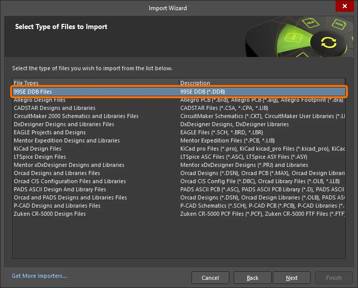
Select 99SE DDB Files in the Import Wizard to import Protel 99SE DDB files.
Import Wizard - 99SE DDB Files
99SE DDB Files
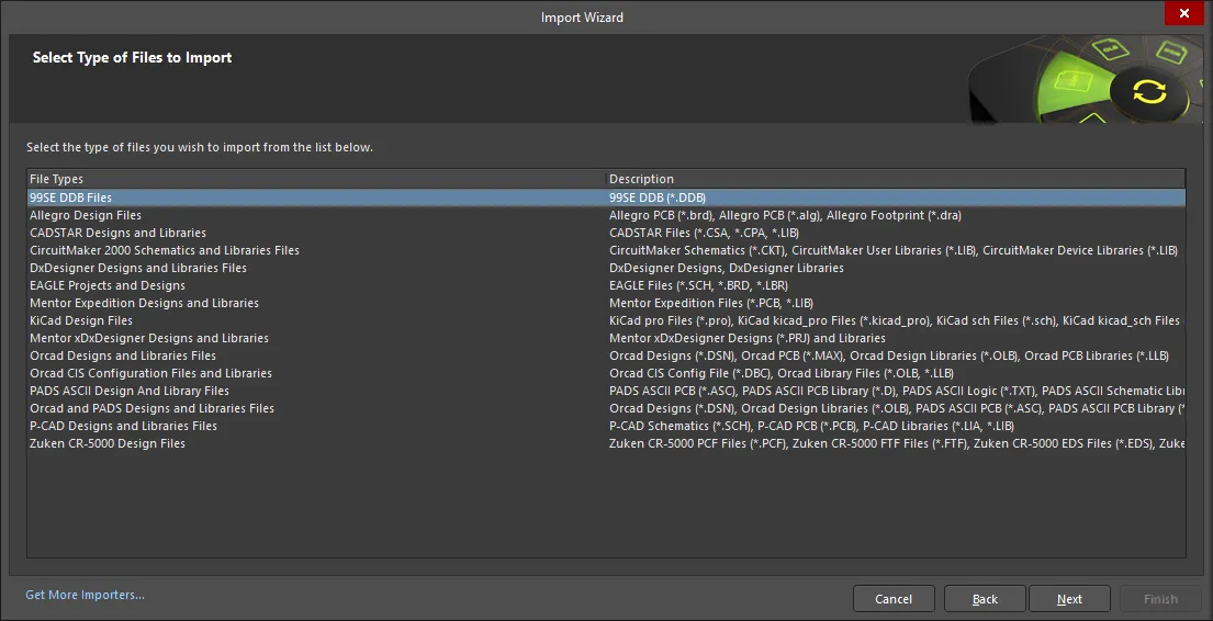
The 99SE DDB import process requires all files, projects and design spaces currently open in Altium Designer to be closed. A dialog will open asking for confirmation.

Click Yes to close all open files and projects; click No to exit the Wizard.
Choosing Files to Import
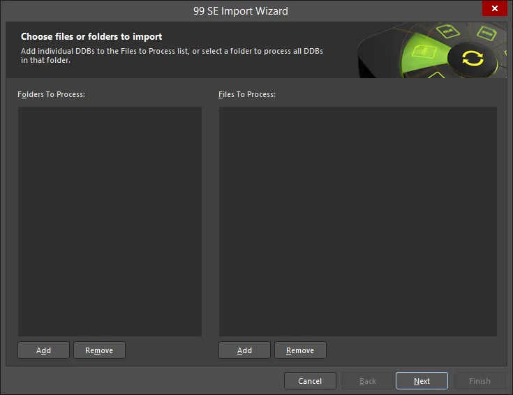
Use this page of the Wizard to select the 99 SE folders or files you want to import. Use the Add button under the Folders To Process region to import all DDB files within the specified folder. Use the Add button under the Files To Process region to import individual DDB files. The Remove button under both regions can be used to delete a selected entry from either region.
Setting File Extraction Options
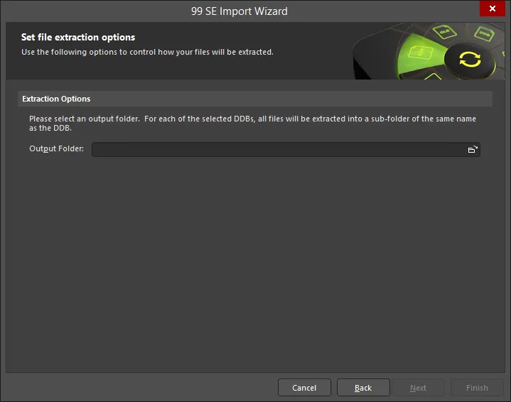
This page of the Wizard allows you to control how your files are extracted. Use  to search for and select the location of the output folder. All files will be extracted into a sub-folder of the same name as the DDB.
Setting Schematic Conversion Options
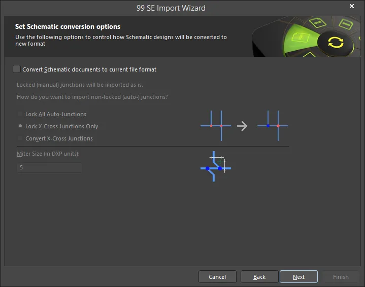
Use this page to control how the schematic designs will be converted.
Enable Convert Schematic documents to current file format if you want the current format to be used. If this option is enabled, locked (manual) junctions will be imported as is. Use the following options to select how to import non-locked (auto) junctions:
- Lock All Auto-Junctions – select this option to lock all auto-junctions.
- Lock X-Cross Junctions Only – select this option to lock only X-Cross junctions.
- Convert X-Cross Junctions – select this option to convert X-Cross junctions.
The 'preview' region on the right dynamically updates depending upon your selection. Locked junctions display as red.
- Miter Size (in DXP units) – if Convert X-Cross Junctions is selected, enter the miter size in the text box.
Setting Import Options
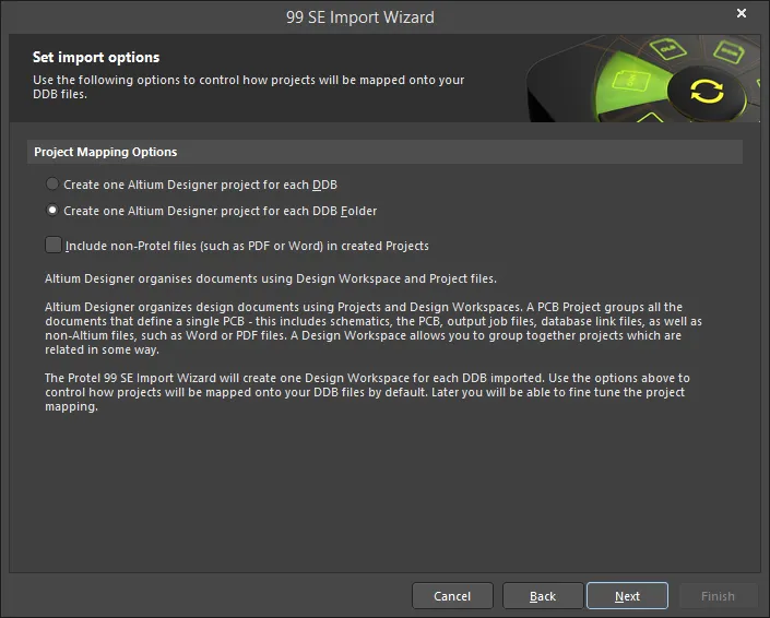
Use the Project Mapping Options on this page to control how projects will be mapped into your database files.
- Create one Altium Designer project for each DDB – select if you typically use one DDB for each board design.
- Create one Altium Designer project for each DDB Folder – select if your DDB contains more than one board design.
- Include non-Protel files (such as PDF or Word) in created Projects – select if you also want to include other file types.
Selecting the Design Files to Import
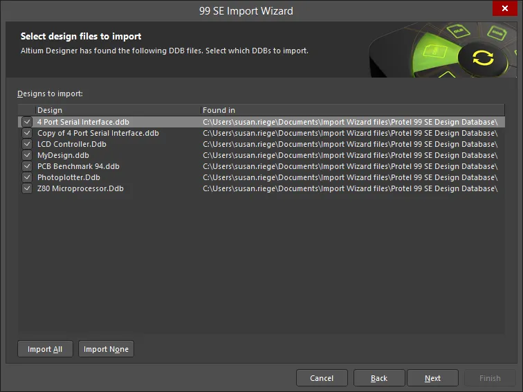
On this page of the Wizard, a list of DDB files appear that Altium Designer has found according to your import settings on previous pages of the Wizard. Enable the checkboxes of the design files you want to import. If you want to import all the displayed files, you also can click Import All to check all boxes. If you want to not import any of the listed files, click Import None to uncheck all boxes.
Review the Project Structure
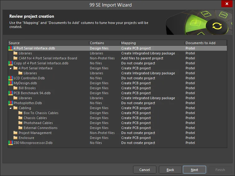
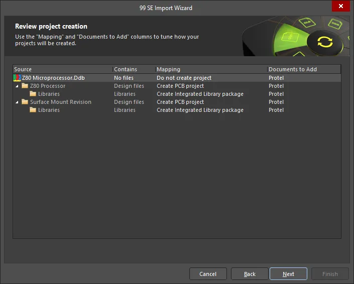
This page of the Wizard can be used to fine tune how your projects will be created. This page displays the assumptions that the Wizard has made about how it should build projects based on the contents of the DDB. Take time to configure these options to ensure you achieve the best result at the completion of the import process. Click in the Mapping column as shown in the following image, then select from a list of available options to change how the selected folder/file is created. Options include:
Do not create project – select to not create a project.Create PCB project – select to create a project.Create Integrated Library package – select to create an integrated library package.Add files to parent project – select to add the files to the parent project.Add files to all projects in DDB – select to add the files to all projects in the DDB.
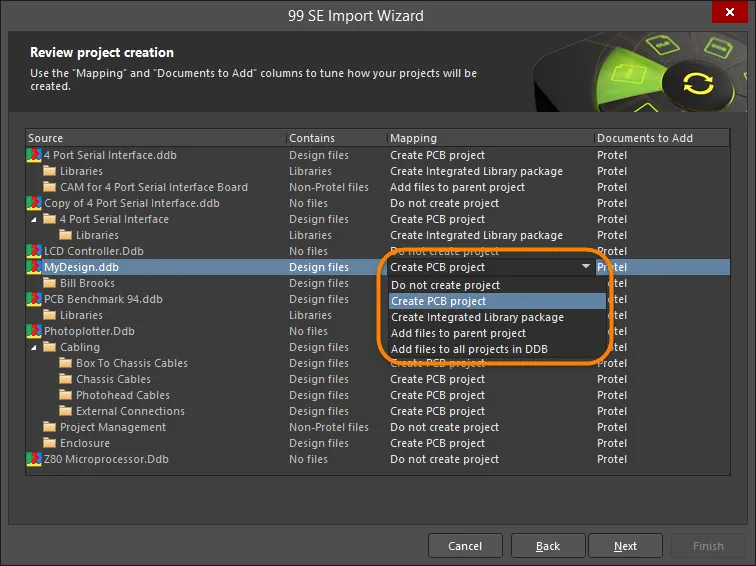
Click in the Documents to Add column to select from a list of available documents to add.
Review the Import Summary
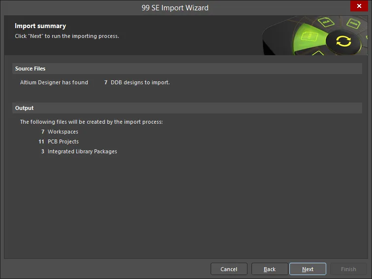
This page of the Wizard shows a summary of the import. The Source Files region shows the number of DDB designs that will be imported. The Output region lists the files that will be created during the import process. This page is useful for ensuring that you have configured your import settings correctly. You can use the Back button if any changes are required.
Click Next to run the import process.
Select the Design Space
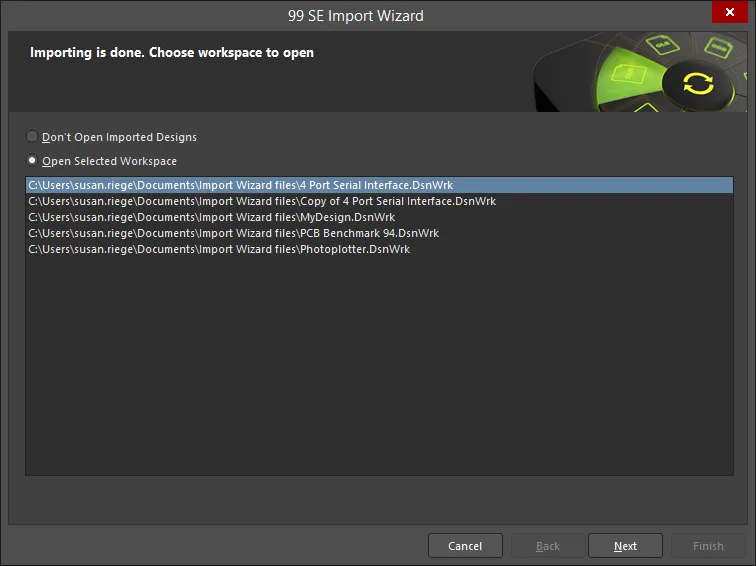
The import process has completed and you can choose whether to open the imported designs on this page. Select Open Selected Workspace, then choose from the listed designs to open a design space. If you do not want to open the imported designs, select Don't Open Imported Designs.
Closing the Wizard
The Wizard has completed successfully. Click Finish to close.
99 SE CAM Manager (*.cam) and Power Print Configuration (*.ppc) files are not recognized by Altium Designer, so outputs will need to be reconfigured for imported designs.
The import process requires all files, projects and project groups that are currently open in Altium Designer to be closed. If this is not the case, you will be prompted to do this first.
The Wizard can be used to import a single DDB or all DDBs in a folder. This document is focused on a single DDB import.
The wizard performs the following steps:
- Extract the files from the database into the nominated folder on your hard drive. Any folder structure within the database will be recreated on the hard drive. All files in the database will be extracted, regardless of whether they are part of the project structure or not.
- Convert schematic documents to the current file format (if this option is enabled).
- Add a recognized file extension to all schematic and PCB files. Altium Designer uses the file extension to recognize which documents it can edit. For schematics, this extension must be Sch, SchDoc, or the original DOS schematic S01, S02, etc naming convention. If there are schematics inside the DDB that do not have an extension,
*.SchDoc will be appended to the filename. Note that this will not break the hierarchy, the Altium Designer compiler will automatically detect this situation and maintain the design hierarchy and connectivity. Note that non-Altium files without a standard file extension will not be automatically renamed.
- Create a project file for each nominated project, of the type PrjPcb (PCB project) or LibPkg (library package), and add the relevant project files.
- Create a project group (
*.DsnWrk), and add all created projects to it.
- Open the project group. When the created project group opens, it will display all the Altium Designer projects that were built. The image above shows the result of importing the Z80 Microprocessor design that is included in the
Protel 99 SE\Examples folder.
Creating the Altium Designer Project(s)
As you work through the pages of the Wizard, you will note that on the Set Import Options page you will be asked if the Wizard should:
- Create one Altium Designer project for each DDB - choose this option if you typically use one DDB for each board design.
- Create one Altium Designer project for each DDB folder - choose this option if your DDB contains more than one board design.
- Select which ever is most appropriate for how you use DDBs. There will be an opportunity to tune the Review Project Creation page later in the wizard.
On the Review project creation page, you will see the assumptions that the Wizard has made about how it should build projects based on the contents of the DDB. Take time to configure these options to ensure you achieve the best result at the completion of the import process.
Once the Wizard is complete, Altium Designer will present the projects and their documents, as shown in the image below. Note that the hierarchy of the schematic project will not be displayed until the project schematics are opened for the first time.
File Format Changes
The file format for schematics, schematic libraries, PCBs and PCB libraries has changed from the formats used in Protel 99 SE. You can open and use 99 SE format schematic and schematic library files directly in Altium Designer, but you will be asked if you wish to convert them whenever you save them. 99 SE PCB files must be converted to the Altium Designer file format before they can be edited. Whenever you open an older format PCB, the PCB Import Wizard will launch and guide you through this process.
The following topics cover various differences in objects and design approaches that it is important to be aware of.
Components
Components have been greatly enhanced in the DXP versions. They now support unlimited component parameters and have an improved model definition and linking system, such as the ability to visually browse for a PCB footprint.
Double-click to edit a component and you will find that all the 99 SE text fields and part fields have been converted to parameters. While 99 SE supported up to eight text fields and 16 part fields per component, Altium Designer has no limit on the number of parameters that can be added.
Parameters can be used for any purpose in an Altium Designer design. They can also be linked to your company database using a DbLink document. Parameters can be included in a report generated from the project. Add an OutJob document to the project and configure the reporting engine to generate a report in the required output format. Parameters can also be used to link to datasheets, or a web URL.
For details on creating components and adding models, see Building & Maintaining Your Components and Libraries.
For more information on linking from the components to a database, see Database Libraries.
For more information on creating a Bill of Materials from your design, see BOM Management with ActiveBOM.
Component Links
You will find that all links between schematic and PCB components are removed when you import a 99 SE design. Re-establishing the component linking is easy, but it must be done based on the designators.
On the PCB side, pair components with footprints in the Component Links dialog (Project » Component Links in the PCB editor main menus). A fully synchronized 99 SE database should make this a two-click process. First, add pairs by matching designators (the default correlation), then perform the update.
An underlying difference between Altium Designer and 99 SE is that establishing links is not a prerequisite to synchronization. If, for example, you skip the steps described above and simply try running update/import commands on a PCB design you brought into Altium Designer from 99 SE, you will be informed that, although synchronization by Unique IDs has failed, you may still proceed to match by designators. Doing so will not have any effect upon the Unique ID fields in your design, meaning that if you repeat the process, the same status will be reported. Assigning the same Unique ID values to schematic components and PCB footprints is the only way to create persistent links between them.
Net Identification Scope
It may be appropriate to assign a specific net identification scope to your schematic projects. By default, this setting in the Project Options dialog will be automatic (based upon design contents). This means that if your project contains any sheet symbols with sheet entries inside, the scope will be set to Hierarchical (Sheet entry <-> port connections, power ports global). If your project contains ports but no sheet entries, then the scope will be set to Flat (Only ports global). If your project contains neither sheet entries nor ports, then net labels will become global.
If you do not wish to use this automatic detection, you may assign an individual scope to be applied to the project regardless of its contents. This is recommended for 99 SE projects that used the Global scope for both ports and net labels, as this scope is not available through Altium Designer's automatic detection.
Note that Altium Designer also supports flat projects, without the use of a top sheet. To explore this option, try removing the top sheet from your flat design. The Altium Designer Navigator panel will show the connective structure in the design, where you can explore the design connectivity.
DXP Import Wizard
The first time you open a legacy board in Altium Designer, the DXP Import Wizard will open to help you make assignments for board shape, split planes and special rule conversions.
Board Shape
All PCB designs in Altium Designer require a board shape. Since this did not exist in earlier versions of Protel, it must be added to boards you bring in from previous versions.
The Import Wizard gives you two options: a rectangular shape encompassing all of your design objects, or a more precise board outline based upon shapes detected within your design. If you choose the latter option, your Keep-Out and Mechanical layers will be analyzed for shapes which might yield a shape for your PCB. Whatever option you choose, a preview pane will show the proposed Board Shape. If none of these appear correct, then choose the rectangular option and then use the Design » Board Shape menu options to configure the board shape in Altium Designer.
The board shape defines the physical extents of the board, and as such, provides the outline for pullback tracks on internal planes. Because planes are negative images, pullback tracks create a thin no-copper ("blowout") zone between the board edge and the plane, preventing shorts along the edge of the manufactured board. These tracks are not accessible for direct editing on the plane layers, but the board shape may be redefined at any time within Altium Designer, and the pullback tracks will be rearranged accordingly. The Layer Stackup Manager will allow you to change the initial pullback distance you set in the Import Wizard.
Split Planes
Altium Designer has changed the way split planes are defined. Previously, each split plane area was placed as a closed region (essentially an empty polygon) on an internal plane layer. In contrast, splitting a plane into separate regions in Altium Designer is a process of defining blowouts (copper-free areas) by placing lines, arcs and fills on the plane layer. Each time you terminate a placement process on a plane layer, the plane is analyzed and all isolated regions are detected. Double-click on a region to assign it to a net. These blowout sections do not belong to one split region or another; Altium Designer designs no longer require overlapping or exactly aligned tracks alongside adjacent split planes. Altium Designer also supports defining nested split regions.
There is one exception to this behavior - the Import Wizard allows you to operate in legacy split plane mode. It is recommended that you only choose this mode if you encounter problems with the import of planes in your design, or if your PCB includes split planes that will require further editing in an earlier version. Later, you may convert your design to Altium Designer plane mode; in the meantime, new split planes must be placed as closed boundaries on internal planes, rather than inferred from blowouts.
When you do convert your designs to the new method, you will be able to simplify your split plane definitions. You don't have to, as your legacy split planes will still work in Altium Designer, but they may include redundant lines that make your board more complex and calculation-intensive than it ought to be. The easiest way to update 99 SE split plane definitions in Altium Designer is to add a new plane layer, then trace the existing regions onto the new plane. Once this is done, select all objects on the old plane layer and delete them. After the net assigned to that layer has been disconnected, the layer can be deleted from the layer stack. Finally, check that the net assignment for each split region is correctly assigned, either by double-clicking on each region, or using the Split Plane Editor in the PCB panel.
From-Tos
From-Tos that have been defined between specific pads in 99 SE will have to be redefined in Altium Designer, so open the Altium Designer PCB panel in From-To Editor mode to do this.
Special Rule Conversions
Some older versions of Protel did not allow pad settings to override general mask expansion rules, meaning that some older designs might have had solder or mask expansion rules that targeted single pads only. The Import Wizard will detect any such rules in your design, and offer to convert them to pad settings, thus simplifying your set of design rules. On the other hand, the Import Wizard will offer to create a new rule disconnecting vias from planes, as some older Protel versions did not allow via-plane connections.
Simulation Model References and Configurations
Specific fields in 99 SE components are reserved for simulation data. When these fields include simulation data, Altium Designer translates their values to the simulation Model linkage for that component.
In 99 SE, all simulation models were contained in the SimulationModels.ddb supplied with the installation. Altium Designer, on the other hand, allows you to include the model in the project, or define a search path for the project if you prefer to keep simulation models in a central location. Yet another approach is to build integrated libraries, where the simulation models are compiled into the integrated library file along with the symbol, the footprint, and any other models linked to the components.
Because all 99 SE components use a defined model path to link from the schematic component to the simulation model, the easiest way to keep your 99 SE simulations working in Altium Designer is to export all the folders and models from the 99 SE simulation models database, into the Library\Sim folder of your Altium Designer installation.
Altium Designer supports referencing a model using a full path. When a 99 SE schematic with simulation-ready components on it is imported, the simulation model link is automatically transferred to the Altium Designer Full Path Model Location field. Altium Designer includes an internal check to always include the Library folder of your Altium Designer installation when searching a full path model location, ensuring that your 99 SE design will simulate once the simulation models are in their new location.
In 99 SE, the settings in the Analysis Setup dialog are stored in a configuration file (*.cfg) within the database. When Altium Designer simulates the design for the first time, if no specific simulation setup parameters have been configured, it will look for and use that *.cfg file. When you save your new Altium Designer project, the simulation settings will be written to the project file and the old *.cfg file becomes redundant.
For details on performing a circuit simulation, see Analyzing Your Design using Circuit Simulation.
Multi-Channel Designs
Perhaps those PCB projects that will require the most attention are your multi-channel designs.
In 99 SE, multi-channel design was really a matter of making copies of the child sheet, which were then re-annotated and referenced by separate sheet symbols. Now that Altium Designer lets you truly reference the same child sheet repeatedly, you will first need to modify your schematics. First, remove all but one of the copied child sheets from your project. Then, update the corresponding sheet symbols with distinct names but all referencing the one remaining child sheet.
A wiser strategy, however, would be to delete all but one sheet symbol for each channel, and replace its Name field with an appropriate Repeat command. This way the number of channels may be changed at any future time by changing this one field.
There are numerous features related to multi-channel design, including the ability to transfer 'channel' information to PCB layout, place and route one channel, and then have the software repeat the placement and routing for all other channels.
For more information on working with a multi-channel design, see Creating a Multi-channel Design.
Design Outputs
The 99 SE CAM Manager (*.cam) and Power Print Configuration (*.ppc) files are not recognized by Altium Designer, so outputs will need to be reconfigured for imported designs.
In Altium Designer, there are two approaches to configuring outputs: settings defined through the Schematic and PCB Editor menus are stored in the Project file, or you can add an Output Job file (*.OutJob) to the project. To learn more about design outputs, see Preparing Your Design for Manufacture.
Transferring a Design Back to 99 SE
Both the schematic and PCB editors support saving schematic, schematic library, PCB and PCB library files in the V4 (99 SE) format. In an Outputjob file, click [Add New Export Output] and select an entry in the Save As/Export PCB or Save As/Export Schematic menu, then double-click the added output to access the Save As / Export Output Setup dialog and choose the required format. The export outputs can then be generated directly from the file or as part of the Project Release process.

Alternatively, use the File » Save As command from the main menu of an appropriate editor and then select the required file format from the Save as type drop-down of the Save As dialog that opens.
Data that can not be transferred back includes:
- New schematic design objects, including notes, compile masks, parameter set objects and offsheet connectors.
- New PCB design objects, including regions, solid polygon pours (the older hatched style polygons can be transferred), the board outline, dimensions, and complex padstacks.
- Design rules that can not map back to 99 SE design rules.
- Split plane definitions (Altium Designer calculates split regions based on objects placed on plane layers; it does not use empty polygons to define split regions).
Importing a Protel DOS Schematic
A Protel DOS Schematic (*.s??) can be imported in Altium Designer. To do this, select the File » Import » Protel DOS Schematic command from the main menus of Altium Designer's schematic editor.
Exporting a PCB to the Protel PCB 2.8 ASCII Format
An active Altium Designer PCB can be exported to the Protel PCB 2.8 ASCII file format (*.PCB). To do this, select the File » Export » Protel PCB 2.8 ASCII command from the main menus of Altium Designer's PCB editor.
Importing a Tango PCB
Altium Designer includes the capability to import a Tango PCB file.
To import a Tango PCB ASCII file (*.PCB) to the active Altium Designer PCB document, select the File » Import » Tango PCB command from the main menus of Altium Designer's PCB editor.
Importing an Autotrax PCB
Altium Designer includes the capability to import an Autotrax PCB file.
To import an Autotrax PCB file (*.PCB), select the File » Open command from the main menus and then browse to and open the file. The DXP Import Wizard will open to configure the import.
P-CAD Design Files Import-Export Support
Importing a P-CAD Design
Translating complete P-CAD designs, including schematics, PCB layout, and library files can all be directly handled by Altium Designer's Import Wizard without converting to ASCII first - thus avoiding the need for having P-CAD installed. The Import Wizard removes much of the headache normally found with design translation by analyzing your files and offering many defaults and suggested settings for project structure, layer mapping, PCB pattern (footprint) naming, and more. Complete flexibility is found in all pages of the wizard, giving you as little or as much control as you would like over the translation settings before committing to the actual translation process.
File Translation
P-CAD design files in the Import Wizard translate as follows:
- P-CAD PCB (
*.PCB) files translate into Altium Designer PCB files (*.PcbDoc).
- P-CAD schematic (
*.SCH) files translate into Altium Designer schematic files (*.SchDoc). Each sheet within a P-CAD schematic file is imported as a single Altium Designer schematic file (*.SchDoc). Design hierarchy is maintained, including complex hierarchy.
- These files will be grouped into an Altium Designer PCB project (
*.PrjPCB) that is automatically created.
- P-CAD PCB files generate an output job document (
*.OutJob) if necessary. This document will contain all the print settings from the P-CAD PCB.
P-CAD library (*.LIB and *.LIA) files translate as follows:
- Libraries that contain solely pattern information translate into Altium Designer PCB library files (
*.PcbLib).
- Libraries that contain both pattern and symbol information translate into both Altium Designer PCB library files (
*.PcbLib), and schematic library files (*.SchLib) respectively.
-
Libraries that contain both component and symbol information translate into Altium Designer schematic library files (*.SchLib). Libraries which contain solely symbol information do not import as Altium Designer does not have the same concept of a symbol as P-CAD (described later).
Translated P-CAD libraries are automatically grouped in an integrated library package (*.LibPkg).
Translation Overview
The steps for translating your P-CAD designs and libraries using the Import Wizard look as described below.
Translating P-CAD Designs
- Import Wizard:
- Select files for translation.
- Map pattern to footprint names. Renaming occurs to cater for:
- Multiple pattern graphics.
- Pin to pad mismatches.
Mapping can be adjusted to suit your requirements.
- Map PCB layers.
- Create Altium Designer project.
- After Import Wizard:
- Set project options. Use the Class Generation tab of the Project Options dialog (Project » Project Options).
- Assign component links to matching PCB and schematic components. Use the Edit Component Links dialog (Project » Component Links). Click the Add Pairs Matched By button.
- Resolve footprint name differences. Use the Differences between dialog (Project » Show Differences). Use right-click menu options to set the Update direction.
- Resolve net name differences. Use the Differences between dialog (Project » Show Differences). Use right-click menu options to set the Update direction.
- Perform synchronization (generate ECOs and apply).
- Perform PCB DRC.
Translating P-CAD Libraries
- Import Wizard:
- Select files for translation.
- Map pattern to footprint names. Renaming occurs to cater for:
- Multiple pattern graphics.
- Pin to pad mismatches.
Mapping can be adjusted to suit your requirements.
- File translation.
- Compile library package and install generated integrated library. Libraries are compiled and validated. Cross-checked for signal pin mapping.
- After Import Wizard:
- Review the Messages panel for warnings or errors.
- Resolve errors and recompile.
- Move/copy new libraries to your preferred storage area.
- Install libraries into Altium Designer (the Components panel).
- Place components from the Components panel.
Using the Import Wizard for P-CAD Files
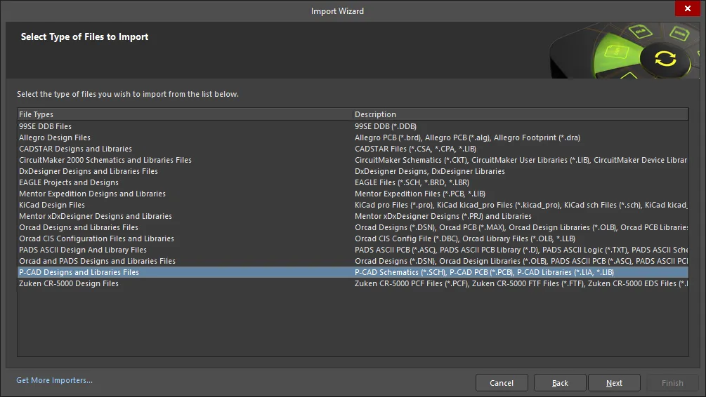
To import P-CAD files, select File » Importer Wizard. On the Select Type of Files to Import page of the Import Wizard, select P-CAD Designs and Libraries Files.
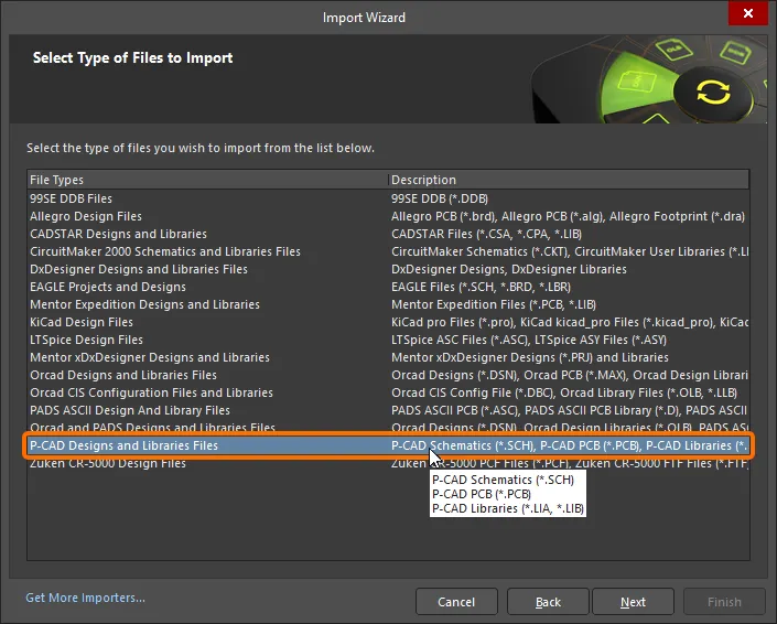
Select P-CAD Designs and Libraries Files in the Import Wizard to import P-CAD files.
Right-mouse command menus are available for further control over the translation process through each page of the wizard.
Import Wizard - P-CAD Designs and Libraries Files
P-CAD Designs and Libraries Files
Translating complete P-CAD designs, including schematics, PCB layout, and library files, can all be directly handled by the Import Wizard without first converting to ASCII – thus avoiding the need for having P-CAD installed. The Import Wizard removes many of the problems normally found with design translation by analyzing your files and offering many defaults and suggested settings for project structure, layer mapping, PCB pattern (footprint) naming, and more. Complete flexibility is found in all pages of the Wizard, giving you as little or as much control as you would like over the translation settings before committing to the actual translation process.
In P-CAD, all design work begins on the sheet, the logical working area of the design. There can be multiple schematic sheets within a single P-CAD schematic design file (*.SCH file). In Altium Designer, the logical design area begins with a document and for each document there is a file stored on the hard drive. This means that for each Altium Designer schematic document (sheet) there is a file – an important conceptual difference to remember.
In P-CAD, components form the basic building blocks of design in P-CAD and the symbol is merely a graphical representation of that component in the schematic. In Altium Designer, the symbol is effectively the component for all phases of design and not just the schematic capture portion of it. A little comparison will help show the differences of how the two are modeled between the respective systems for a better understanding.
Select the P-CAD Design Files to Import
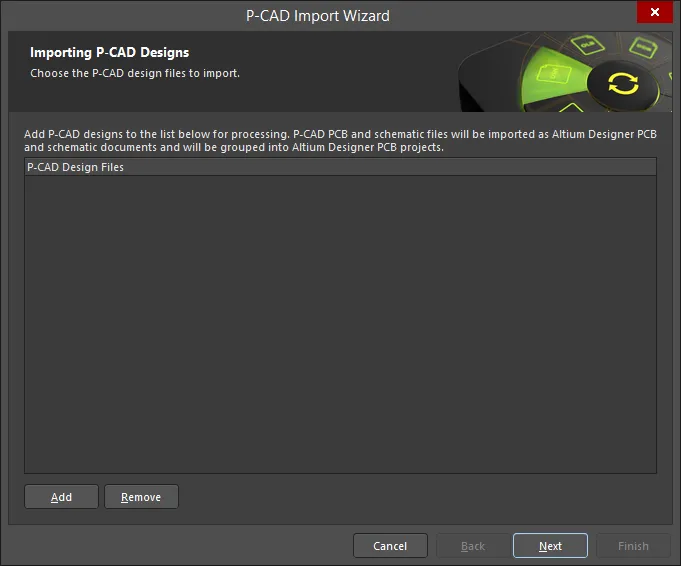
Click Add to choose which P-CAD design files to include in the process. You can delete a selected file by clicking Remove.
Select the P-CAD Library Files to Import
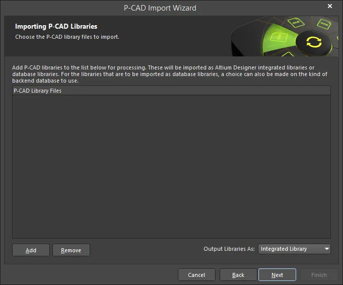
Click Add to choose which P-CAD library files (LIB and LIA) to include in the process. You can delete a selected file by clicking Remove.
You can select what type of libraries to create using the Output Libraries As drop-down. Choices include:
Integrated LibraryDBLib (Access Backend)DBLib (CSV Backend)
A progress window will open and close quickly before the next page of the Wizard appears.
PCB Footprint Naming Format
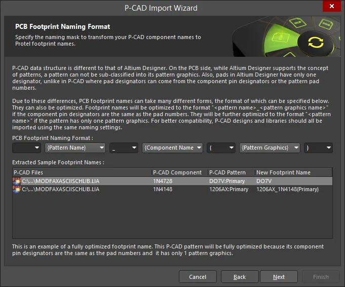
P-CAD data structure is different than that of Altium Designer. On the PCB side, Altium Designer supports the concept of patterns, a pattern cannot be sub-classified into its pattern graphics in P-CAD. Additionally, pads in Altium Designer have only one designator, while in P-CAD where pad designators can come from the component pin designators or the pattern pad numbers.
Due to these differences, PCB footprint names can take many different forms. The PCB Footprint Naming Format page is used to specify the format of the PCB footprints.
Use the drop-downs to select the PCB Footprint Naming Format. The Extracted Sample Footprint Names region dynamically updates according to your selections.
Schematic Component Naming Format
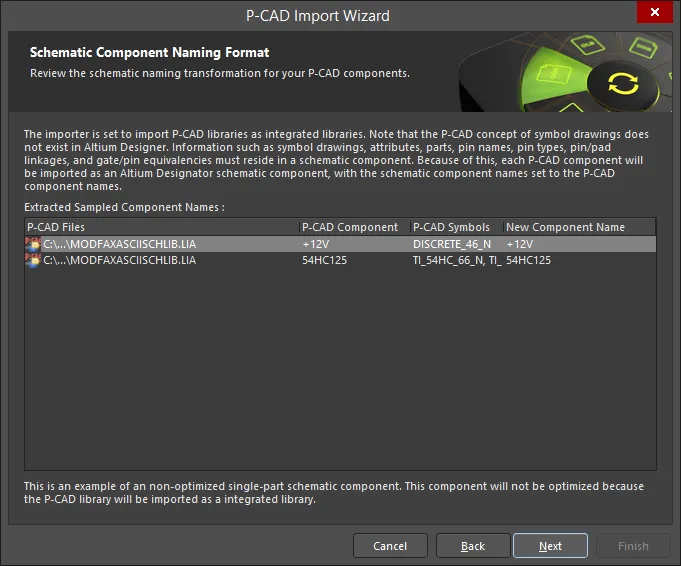
Use this page of the Wizard to review the schematic naming transformations for your P-CAD components. The P-CAD concept of symbol drawings does not exist in Altium Designer. Information such as symbol drawings, attributes, parts, pin names, pin/pad linkages, and gate/pin equivalencies must reside in a schematic component. As a result of this, each P-CAD component will be imported as an Altium Designer schematic component, with the schematic component names set to the P-CAD component names.
Reporting Options
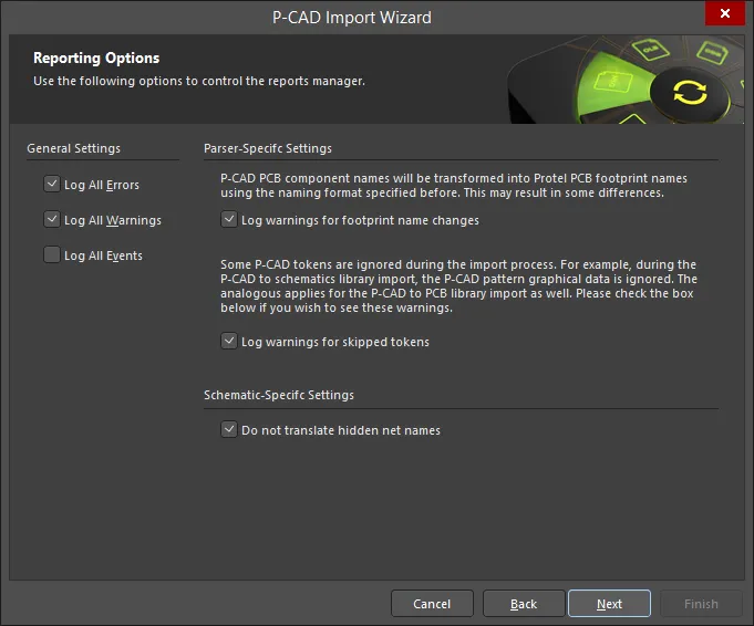
Use the Reporting Options page to set up general log reporting options.
Under General Settings, enable the desired options: Log All Errors, Log All Warnings, Log All Events.
P-CAD PCB component names will be transformed using the settings specified on the PCB Footprint Naming Format page, which may result in some differences. Enable Log warnings for footprint name changes in order to see these differences.
Enable Log warnings for skipped tokens to see warnings regarding P-CAD tokens that were ignored during the import process.
Enable Do not translate hidden net names if desired.
Current Layer Mappings
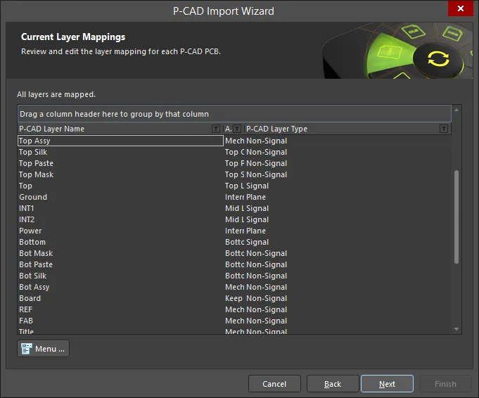
If desired, you can edit the layer mapping for any or all P-CAD PCBs on this page of the Wizard. Use the drop-downs to the right of each header to select. To group by a column, drag the column header into the area at the top of the table specified.
Use the Menu button to manipulate the layer mappings.
- Invert Selection – select to invert the items that are selected to not selected, and those that are not selected to selected.
- Set Selection To – select to access a sub-menu of layer types from which you can choose the desired layer.
- Load Layer Mapping – select to open the Load Configuration dialog to load the desired mapping files.
-
Save Layer Mapping – select to open the Choose File to Save Layer Mapping dialog and choose the path in which to save the layer mapping.
Right-clicking in the grid region gives access to the same menus and sub-menus as clicking the Menu button.
Output PCB Projects
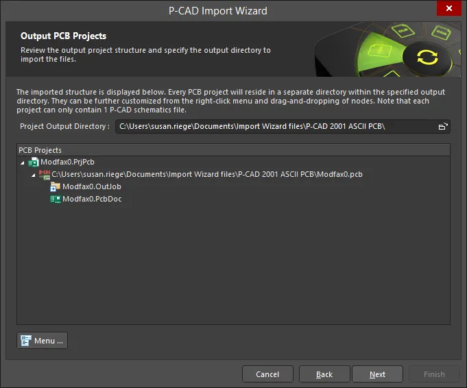
Use this page of the Wizard to review the output project structure and specify the output directory in which to import the files. Use the Browse Folder icon to search for and choose the Project Output Directory.
- Menu
- Rename Project – click to rename the selected project. This option is available only when a
*.PrjPcb file is selected.
- Remove Selected Projects – click to remove the selected project from the PCB Projects structure.
- Reset Structure to Default – click to reset the PCB Projects structure to the defaults.
- Add Designs to Project – click to add a design(s) to the project. This option is available only when a
*.PrjPcb file is selected.
- Remove Selected Designs - click to remove the selected design files.
Right-clicking in the PCB Projects region gives access to the same menus and sub-menus as clicking the Menu button.
Output Integrated Libraries
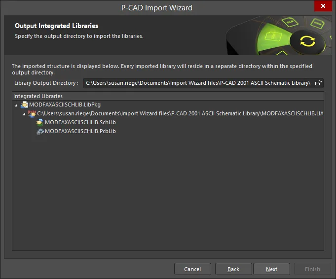
The output directory for the imported libraries is shown on this page of the Wizard. Use the Browse Folder icon to search for and choose the desired directory.
Executing Import Process
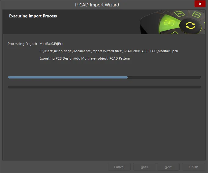
On this page of the Wizard, a green progress bar shows the progress of the import process while also listing each file at the process continues.
Closing the Wizard
The P-CAD Import Wizard has completed. Click Finish to close the Wizard.
Imported P-CAD files:
P-CAD design files translate as follows:
- P-CAD PCB (*.PCB) files translate into Altium Designer PCB files (*.PcbDoc).
- P-CAD schematic (*.SCH) files translate into Altium Designer schematic files (*.SchDoc). Each sheet within a P-CAD schematic file is imported as a single Altium Designer schematic file (*.SchDoc). Design hierarchy is maintained including complex hierarchy.
- The files will be grouped into an Altium Designer PCB project (*.PrjPCB) that is automatically created.
- P-CAD PCB files generate an output job document (*.OutJob) if necessary. This document will contain all the print settings from the P-CAD PCB.
P-CAD library (*.LIB and *.LIA) files translate as follows:
- Libraries that contain only pattern information translate into Altium Designer PCB library files (*.PcbLib).
- Libraries that contain both pattern and symbol information translate into both Altium Designer PCB library files (*.PcbLib) and schematic library files (*.SchLib).
-
Libraries that contain both component and symbol information translate into Altium Designer schematic library files (*.SchLib).
Libraries that contain only symbol information do not import as Altium Designer does not have the same concept of a symbol as P-CAD.
- Translated P-CAD libraries are automatically grouped in an integrated library package (*.LibPkg).
Working with Documents
In P-CAD, all design work begins on the sheet, the logical working area of the design. There can be multiple schematic sheets within a single P-CAD schematic design file (*.SCH file).
In Altium Designer, the logical design area begins with a document, and for each document there is a file stored on the hard drive. This means that for each Altium Designer schematic document (sheet) there is a file, an important conceptual difference to remember.
There can also be multiple design documents of varying types depending on the nature of the design you'll be working on. Getting started, most P-CAD users will be interested in the schematic and PCB document types as these are the files that their designs will be translated to.
New schematic and PCB document types can easily be created via the File » New menu, or by right-clicking on the project in the Projects panel.
The Schematic Symbol Is the Component...
As an expert P-CAD user, you'll know that components form the basic building blocks of design in P-CAD, and the symbol is merely a graphical representation of that component in the schematic. But in Altium Designer the symbol is effectively the component for all phases of design, and not just the schematic capture portion of it. A little comparison will help show the differences of how the two are modeled between the respective systems for a better understanding.
P-CAD Components and Altium Designer Components
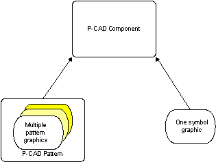
P-CAD components have a single symbol graphic and one or more pattern graphics for each pattern
In P-CAD, all of the logical and electrical data that is held in the component can be seen in Library Executive in the Pins View dialog. Pin and gate swapping component pin to symbol pin, and pattern pad mapping, along with the pin's electrical and logical data is the only component information available. Because this information relates primarily to the pins and is somewhat limited, there are inherent restrictions to the number of ways that P-CAD components can be represented throughout the design process. An Altium Designer component, on the other hand, contains more information and is more flexible in terms of how it can be represented.
In Altium Designer, the logical symbol is assumed to be the essential starting point of a component. It can be initially defined at minimum as a name in a schematic library to which pins and any graphical symbols or alternative display options needed for implementation may be added. This flexibility allows a component to be represented in different ways during the design and capture process. This may not only be as a logical symbol on the schematic, but also be a footprint on the PCB or even as a SPICE definition for simulation.
The fundamentals of how components are defined, their properties, and basic relationships between components, models and library concepts are explained further in Building & Maintaining Your Components and Libraries.
Importing a P-CAD PDIF File
A P-CAD PDIF file (*.PDF) can be imported in Altium Designer. To do this, select the File » Import » P-CAD PDIF command from the main menus of Altium Designer's PCB editor.
Exporting a Schematic or Schematic Library to the P-CAD V16 Format
An Altium Designer schematic can be exported to the P-CAD V16 ASCII Schematic Design file format (*.sch). In an Outputjob file, click [Add New Export Output] and select an entry in the P-CAD V16 ASCII Schematic Design menu. The export outputs can then be generated directly from the file or as part of the Project Release process.
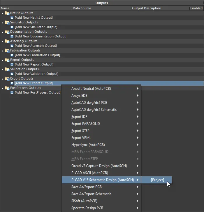
Alternatively, select the File » Export » P-CAD V16 ASCII Schematic Design command from the main menus of Altium Designer's schematic editor.
To export an Altium Designer schematic symbol library to the P-CAD V16 Schematic library (*.lia) file format, select the File » Export » P-CAD V16 Schematic library command from the main menus of Altium Designer's schematic symbol editor.
Exporting a PCB or PCB Library to the P-CAD Format
An Altium Designer PCB can be exported to the P-CAD ASCII file format (*.PCB). In an Outputjob file, click [Add New Export Output] and select an entry in the P-CAD ASCII (AutoPCB) menu. The export outputs can then be generated directly from the file or as part of the Project Release process.
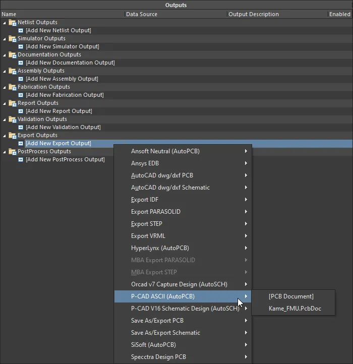
Alternatively, select the File » Export » P-CAD ASCII command from the main menus of Altium Designer's PCB editor.
To export an Altium Designer PCB footprint library to the P-CAD V16 PCB library (*.lia) file format, select the File » Export » P-CAD V16 PCB Library command from the main menus of Altium Designer's PCB footprint editor.
