Chinese - Translation is available for Altium Designer 22:
Go to the pageParent page: High Speed Design
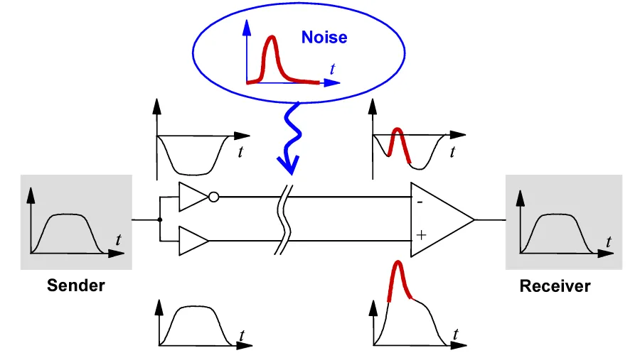
Differential pair routing is a design technique employed to create a balanced transmission system able to carry differential (equal and opposite) signals across a printed circuit board. Typically this differential routing will interface to an external differential transmission system, such as a connector and cable.
A differential signaling system is one where a signal is transmitted down a pair of tightly coupled carriers, one of these carrying the signal, the other carrying an equal but opposite image of the signal. Differential signaling was developed to cater for situations where the logic reference ground of the signal source could not be well connected to the logic reference ground of the load. Differential signaling is inherently immune to common mode electrical noise, which is the most common interference artifact present in an electronic product. Another major advantage of differential signaling is that it minimizes electromagnetic interference (EMI) generated from the signal pair.
Differential pair PCB routing is a design technique employed to create a balanced transmission system able to carry differential (equal and opposite) signals across a printed circuit board. Typically this differential routing will interface to an external differential transmission system, such as a connector and cable.

It is important to note that while the coupling ratio achieved in a twisted pair differential cable may be better than 99%, the coupling achieved in differential pair routing will typically be less than 50%. Current expert opinion is that the PCB routing task is not to try to ensure a specific differential impedance is achieved, rather, to focus on ensuring the differential signal arrives in good condition at the target component as it travels from the external cabling.
According to Lee Ritchey, a noted industry high-speed PCB design expert, successful differential signaling requires:
- To set each of the routing signal impedances to half the incoming differential cable impedance.
- That each of the two signal lines is properly terminated in its own characteristic impedance at the receiver end.
- That the two lines should be of equal length, to within tolerances of the logic family and the circuit frequency used in the design. The focus should be on preserving the timing; match the lengths close enough to satisfy the skew budget of the design. Example length tolerances include high-speed USB, length mismatch should be no greater than 150 mils; DDR2 clocks need to be matched to within 25 mils.
- Use the benefit of routing the two signals side-by-side to help achieve good quality routing of matched lengths. Where required, it is acceptable to separate to route around obstacles.
- Layer changes are acceptable as long as the signal impedances are maintained.
Transferring the Differential Pairs to the PCB Editor from Schematics
If you have placed Differential Pair directives on nets in the schematic, the default project options settings will result in the differential pairs members being created on the PCB. The following options in the Options for PCB Project dialog are used to configure this:
- Comparator tab - Extra Differential Pairs (then the Different Differential Pair checks for subsequent updates, and the Rules options if you are also creating/changing design rules)
- ECO Generation tab - Add Differential Pair (then the Change Differential Pair checks for subsequent updates, and the Rules options if you are also creating/changing design rules)
- Class Generation tab - Generate Net Classes (if you are also creating a Net Class to use to scope a PCB Differential Pair Routing rule)
Viewing and Managing Differential Pairs on the PCB
Differential pair definitions are viewed and managed in the PCB panel set to Differential Pairs Editor mode. The image below shows the pairs that belong to the Differential Pair Class ROCKET_IO_LINES. Pair V_RX0 is highlighted; the nets in this pair are V_RX0_N and V_RX0_P. The - and + displayed next to each member's net name is a system flag indicating if it is the positive or negative member of the pair.
 Differential pairs can be viewed and managed in the Differential Pair Editor. Right-click in the Differential Pair Classes region to create a new class.
In the PCB panel’s Differential Pairs Editor mode, its three main regions change to reflect the differential pair hierarchy of the current PCB design (in order from the top):
- Differential Pair Classes.
- Individual member Differential Pairs within a class.
- The constituent Nets (negative and positive) that form a differential pair.
Defining a Differential Pair Class
Often there is more than one differential pair that needs to be targeted by a design rule. In this situation, you can define classes of differential pairs, clustering them into logical groups. Right-clicking on a differential pair class entry then selecting Properties (or double-clicking on the entry directly) will open the Edit Object Class dialog in which you can rename or view/modify the differential pair membership of the class. For full control and editing of all classes, including Differential Pair Classes, open the Object Class Explorer dialog using the Design » Classes command from the main menus.
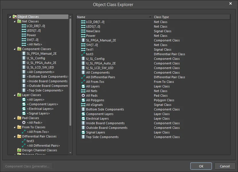
The Object Class Explorer allows creating, viewing and modification for all classes, including Differential Pairs.
Managing Differential Pairs
Differential pairs can be defined on the schematic and also in the PCB Editor. Management in the latter is performed from the Differential Pairs region of the PCB panel, when configured in its Differential Pairs Editor mode. For the particular differential pair class selected, all currently defined differential pair objects that belong to that class will be listed in the Differential Pairs region.

Use the buttons below the region to manage your differential pairs as needed:
- To create a new differential pair object, click the Add button. In the resulting Differential Pair dialog, select existing nets for both the positive and negative nets, give the pair a name then click OK.
Note that only available nets are listed for selection. Nets currently defined as part of existing differential pairs are not listed.
 Quickly create pairs from the named nets.
- To modify an existing differential pair, select its entry and click the Edit button. The Differential Pair dialog will open with the currently chosen nets for the pair entered into the Positive Net and Negative Net drop-down fields. Change one or both nets for the pair or rename the pair as required.
You can also right-click on a differential pair entry, then select Properties, or double-click on the entry directly.
- To delete an existing differential pair, select its entry and click the Delete button.
Creating Differential Pairs from Design Nets
If you are pairing nets that have a consistent naming scheme (i.e. they have a common prefix and a consistent positive/negative suffix, for example, TX0_P and TX0_N), you can use the Create Differential Pairs From Nets dialog. Click the Create From Nets button in the PCB panel in Differential Pairs Editor mode to open the dialog.

Prospective differential pair objects are listed for creation in response to the filter entries at the top of the dialog.
The effectiveness of this automated method directly depends on the naming convention that has been used for the specific nets that will make up the differential pairs. Ideally, a naming convention will be used so that a common root is followed by a consistent positive/negative indicator (P and N). For example, consider the receiver signal D_ETH_O.RX, which is a differential signal in the design. The two nets that constitute this signal are ETH_O.RX_P and ETH_O.RX_N - these represent the positive and negative sides of the signal, respectively.
The filters at the top of the dialog enable you to quickly target these nets in terms of the net class to which they belong and the particular differentiating factor that has been used to distinguish the positive and negative nets in an intended pairing, for example, _P and _N. You can also define a prefix to be added to the differential pair objects created, and also determine in which differential pair class they are to be added.
For each differential pair object, the dialog lists its constituent positive and negative nets. By default, all prospective differential pair objects are selected for creation and individual ones can be excluded by clearing the associated Create check box.
When all options are set as required, click the Execute button - the differential pair objects will be created and the PCB panel will update accordingly.
- Right-clicking on a Net(s) entry in the PCB panel then selecting Properties (or double-clicking on the entry directly) will open the Edit Net dialog in which you can view/modify the properties of the net as required.
- Use the Rule Wizard button to access the Differential Pair Rule Wizard and implement the differential pair rule properties in an automated process. Refer to the Using the Differential Pair Rule Wizard to Define the Rules section below to learn more.
Using xSignals with Differential Pairs
Main page: Defining High Speed Signal Paths with xSignals
If your differential pairs have series components in the signal path, you might find it worthwhile to create xSignals. An xSignal is a designer-defined signal path between two nodes. They can be two nodes within the same net or they can be two nodes in different nets. Using an xSignal, you can define the signal path so that it includes the net on either side of a series component. Route length calculations for xSignals include the length of the path through the series component, as shown by the thin line that is displayed when an xSignal is selected in the xSignals mode of the PCB panel.
 These differential pairs have been defined as xSignals; the route length includes the series component.
Applicable Design Rules
To interactively route a differential pair, create and configure the following two design rules in the PCB Rules and Constraints Editor dialog (Design » Rules):
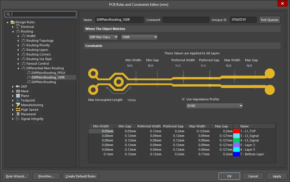
- Differential Pairs Routing - defines the routing width of the nets in the pair, the separation (gap) between the nets in the pair, and the overall uncoupled length (the pair becomes uncoupled when the gap is wider than the Max Gap setting). Set the scope of this rule to target objects that are a differential pair, e.g.,
IsDifferentialPair or InDifferentialPairClass('All Differential Pairs'). Note that the Min/Preferred/Max Gap settings can be used during routing but not during design rule checking. During design rule checking, the distance between the nets in a pair is tested by the applicable Electrical Clearance design rule, as explained in the highlight box below.
- Electrical Clearance - defines the minimum clearance between any two primitive objects (e.g., pad-pad, track-pad) on either any net, the same net, or between different nets. Set the scope of this rule to target objects that are members of a differential pair, e.g.,
InDifferentialPair, and select the appropriate object types In the constraints region of the dialog, as shown below.

Important Note: As you route a differential pair, the routed nets in the pair will be separated by the current Min/Preferred/Max Gap setting defined in the applicable Differential Pair Routing design rule (press Shift+6 to cycle through the Gap modes during routing, check the Status bar to see which mode is being applied). However, during design rule checking, all electrical objects will be tested using the applicable Electrical Clearance design rule, so if the gap value used for routing the differential pair is less than the minimum allowed clearance between the differential pair nets set by the Electrical Clearance design rule, a violation of the Electrical Clearance design rule will occur. If the nets in the pair are placed closer together than the minimum setting allowed by the applicable Electrical Clearance design rule, you will need to add an additional Electrical Clearance design rule targeting the differential pairs, allowing them to have a clearance equal to the Diff Pair Routing Gap setting. This rule should also have the setting that defines the Net types to be tested set to Same Differential Pair, as shown in ![]() this image.
this image.
Setting the Scope of the Design Rules
The scope of the design rule defines the set of objects to which you want the rule applied. Since a differential pair is an object, you can use queries like the following examples:
- InAnyDifferentialPair - is the object in any differential pair.
- InDifferentialPair('D_V_TX1') - targets both nets in the differential pair named
D_V_TX1.
- InDifferentialPairClass('ROCKET_IO_LINES') - targets all nets in all pairs belonging to the differential pair class called
ROCKET_IO_LINES.
- (IsDifferentialPair And (Name = 'D_V_TX1')) - targets the differential pair object that has a name of
D_V_TX1.
- (IsDifferentialPair And (Name Like 'D*')) - targets all differential pair objects whose name starts with the letter
D.
Using the Differential Pair Rule Wizard to Define the Rules
While rules can be created manually using the PCB Rules and Constraints Editor (Design » Rules), the PCB panel in Differential Pairs Editor mode offers the convenience of the Differential Pair Rule Wizard. Use the Rule Wizard button (below the Nets region in the PCB panel) to access the Wizard and implement the rule properties as required.
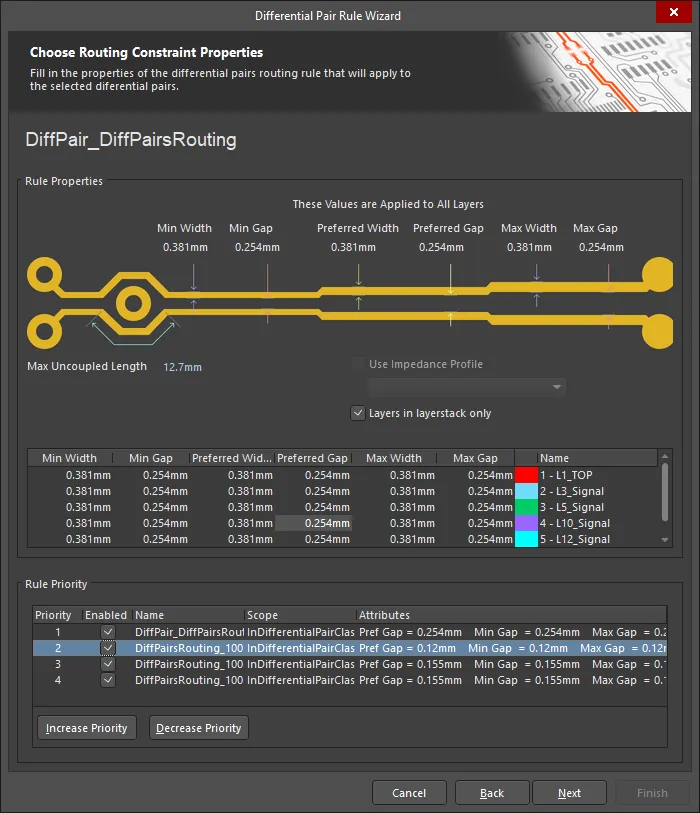
The Differential Pair Rule Wizard guides you through the rule definition process.
Note that the scope of the rules will depend on the selection in the PCB panel prior to launching the wizard, as follows:
Differential Pair Class
If the All Differential Pairs class is selected, the scope will be All for each rule.
If a specific differential pair class is selected, the scope will be InDifferentialPairClass('ClassName') for each rule.
Differential Pair
If a single differential pair object is selected in the panel, the scopes will be:
- Width -
InDifferentialPair('PairName')
- Matched Net Lengths and Differential Pairs Routing -
IsDifferentialPair And (Name = 'PairName'))
If multiple differential pair objects are selected in the panel, there will be individual scope entries for each pair object, each separated by an 'Or' operator. For example, a routing Width rule targeting individually selected differential pair objects D_ETH_O.TX and D_ETH_O.RX will have a scope of:
InDifferentialPair('D_ETH_O.TX') Or InDifferentialPair('D_ETH_O.RX')
Note that the clearance from a net in a differential pair to any other electrical object that is not a part of the pair is monitored by the applicable Clearance rule.
Routing a Differential Pair
Related page: Interactive Routing
Differential pairs are routed as a pair - that is, you route two nets simultaneously. To route a differential pair, select Interactive Differential Pair Routing from the Route menu or the Active Bar. You will be prompted to select one of the nets in the pair; click on either to start routing. It doesn't matter if the positive or negative trace in a pair is selected as the system will automatically select the other trace too. The video below shows a differential pair being routed.
During differential pair routing, you can perform the following functions:
- Shift+R to cycle through the conflict resolutions routing modes (Walkaround, Push, Hug and Push, Stop at First Obstacle, Ignore Obstacles).
- Shift+Spacebar to cycle through the available corner styles (45 degree corner, 45 degree arc in corner, 90 degree corner, 90 degree arc in corner).
- Press Spacebar to toggle between the two corner direction sub-modes.
- Press the Backspace key to remove the last vertex.
- Press 3 to cycle possible diff pair routing widths (User Choice, Rule Min, Rule Preferred, Rule Max).
- Press Shift+6 to cycle possible diff pair gaps (Rule Min, Rule Preferred, Rule Max).
- Use the + and - keys on the numeric keypad to switch routing layers.
- To switch layers and insert vias: Press the * key on the numeric keypad or use the Ctrl+Shift+Wheel Scroll shortcut combination; then
- Press 4 to cycle possible via sizes (User Choice, Rule Min, Rule Preferred, Rule Max)
- Press 5 to cycle possible via patterns during a layer change
- Press 6 to cycle possible via stacks, or press 8 to display a list to select from (learn more about controlling the vias placed during interactive routing)
- Shift+F1 to display all of the available in-command shortcuts.
- In the arc in corner modes, press the "," key to decrease the maximum arc radius, and the "." key to increase the maximum arc radius. The arc size can be changed interactively by moving the cursor. The setting defines the maximum allowable arc radius, which is displayed on the Status bar when you are routing.
When using the Interactive Differential Pair Routing tool, note that coupling the differential pair has priority. Therefore, the
SMD To Corner and
SMD Entry design rules might not work as expected. If strict respect for these rules is required when routing a differential pair, use the
Quick Differential Pair Routing tool.
Many of the settings, such as the current routing mode, width, gap and via size, are displayed on the Status bar (shown below) or the Heads Up Display (Shift+H to toggle it on/off).

Many of the differential pair routing behaviors are the same as single-net interactive routing.
► Learn more about Interactive Routing
Configuring the Interactive Differential Pair Router
Many of the interactive differential pair routing settings can be changed during interactive differential pair routing, in the Interactive Differential Pair Routing mode of the Properties panel. Press Tab during routing to display the panel.
To recognize the members in a differential pair, the concept of Coupling is used. When the software recognizes objects that belong to a differential pair it will attempt to drag the pair's partner track or via if the Keep Coupled option is enabled in the Interactive Sliding or the Interactive Via Dragging modes of the Properties panel (which are described below).
The following collapsible sections contain information about the options and controls available:
Net Information
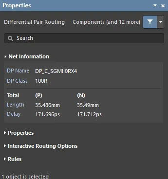
- DP Name – displays the differential pair name.
- DP Class – displays the differential pair class that the routing belongs to (if it is a member of a differential pair class).
- Selected
- Length – the total length sum of the selected segments.
- Delay – the total delay of the selected segments, including those unrouted.
- Total
- Length – the total Signal Length. The Signal Length is the accurate calculation of the total node-to-node distance. Placed objects are analyzed to resolve stacked or overlapping objects and wandering paths within pads, and via lengths are included. If the net is not completely routed, the Manhattan (X + Y) length of the connection line is also included.
- Delay – the delay of the routed segments of the Total Length.
Select the clickable links of the
DP Name,
DP Class,
Length, and
Delay from the
Differential Pair Routing mode of the
Properties panel to be redirected to the
PCB – Nets panel, where you may view and change the details of the nets associated.
Properties

- Layer – use the drop-down to specify on which layer the routing is located.
- Gap – use the drop-down or the Shift+6 shortcut to cycle through the permissible clearances.
- Min – select to specify the minimum permissible clearance between primitives on different nets within the same differential pair.
- Preferred – select to specify the preferred clearance between primitives on different nets within the same differential pair.
- Max – select to specify the maximum permissible clearance between primitives on different nets within the same differential pair.
- Via – if the via is associated with a template, the template name is displayed here.
- Via Diameter – specify the via diameter.
- Via Hole Size – specify the via hole size.
- Width – use the drop-down to specify the width.
- Min – signifies that the design rule minimum width defined for the current net will be used
- Preferred – signifies that the design rule preferred width defined for the current net will be used.
- Max – signifies that the design rule maximum width defined for the current net will be used.
Interactive Routing Options
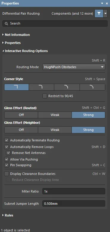
- Routing Mode – use the drop-down or use the Shift+R shortcut to cycle through the desired routing modes. The following choices are available:
Ignore Obstacles – select to ignore existing objects (routing can be freely placed). Violations are highlighted.Walkaround Obstacles – select to have the Interactive Router route around existing tracks, pads and vias. If this mode cannot walk around an obstacle without causing a violation, an indicator appears to show that the route is blocked.Push Obstacles – select to have the Interactive Router move existing tracks out of the way. This mode can also push vias to make way for the new routing. If this mode cannot push an obstacle without causing a violation, an indicator appears to show that the route is blocked.HugNPush Obstacles – select to have the Interactive Router hug existing tracks, pads, and vias as closely as possible and where necessary, push obstacles to continue the route. If this mode cannot hug or push an obstacle without causing a violation, an indicator appears to show that the route is blocked.Stop At First Obstacle – in this mode, the routing engine will stop at the first obstacle that gets in the way.AutoRoute Current Layer – select to enable auto-routing only on the current layer.AutoRoute MultiLayer – select to enable auto-routing on multiple layers.
- Corner Style – select the desired routing corner style or use the Shift+Spacebar shortcut to cycle through the corner styles.
- Restrict to 90/45 – enable to restrict the routing to 90 degrees and 45 degrees only.
- Gloss Effort (Routed) – select the desired gloss level from the panel or use the Shift+Ctrl+G shortcut to cycle through the following choices:
- Off – in this mode, glossing is essentially disabled. Note, however, that cleanup is still run after routing/dragging occurs to eliminate, for example, overlapping track segments. This mode is typically useful at the end stage of board layout when the ultimate level of fine-tuning is required (for example, when manually dragging tracks, cleaning pad entries, etc.).
- Weak – in this mode, a low level of glossing is applied with the Interactive Router considering only those tracks directly connected to or in the area of the tracks that you are currently routing (or tracks/vias being dragged). This mode of glossing is typically useful for fine-tuning track layout or when dealing with critical traces.
- Strong – in this mode, a high level of glossing is applied with the Interactive Router looking for shortest paths, smoothing out tracks, etc. This mode of glossing is typically useful in the early stages of the layout process when the aim is to get a good amount of the board routed quickly.
- Gloss Effort (Neighbor) – select the desired gloss level to apply to traces being pushed by the net currently being routed directly from the panel through the following choices:
- Off – in this mode, glossing is essentially disabled. Note, however, that cleanup is still run after routing/dragging occurs to eliminate, for example, overlapping track segments. This mode is typically useful at the end stage of board layout when the ultimate level of fine-tuning is required (for example, when manually dragging tracks, cleaning pad entries, etc.).
- Weak – in this mode, a low level of glossing is applied with the Interactive Router considering only those tracks directly connected to or in the area of the tracks that you are currently routing (or tracks/vias being dragged). This mode of glossing is typically useful for fine-tuning track layout or when dealing with critical traces.
- Strong – in this mode, a high level of glossing is applied with the Interactive Router looking for shortest paths, smoothing out tracks, etc. This mode of glossing is typically useful in the early stages of the layout process when the aim is to get a good amount of the board routed quickly.
- Automatically Terminate Routing – when enabled, when you complete a route to the target pad, the routing tool does not continue in routing mode from the target pad but rather resets and is ready for you to click on the next source pad from which to route. If this option is disabled, after you route to the target pad, the tool will remain in routing mode and use the previous target pad as the source for the next route.
- Automatically Remove Loops – enable to automatically remove any redundant loops that are created during manual routing. This allows you to re-route a connection without having to manually remove redundant tracks. However, there are times when you need to route nets, such as power nets and when you need loops; you can toggle this option for a selected net by using the Shift+D shortcut to override this global setting for the same net.
- Remove Loops With Vias – enable this option to automatically remove loops with vias. Disable this option for vias to remain during loop removal.
- Remove Net Antennas – enable this option to remove any track or arc end that is not connected to any other primitive and forms an antenna.
- Allow Via Pushing – check this option to allow pushing a Via when in Push Obstacles or HugNPush Obstacles mode.
- Pin Swapping – check this option to enable pin swapping or use the Shift+C shortcut.
- Display Clearance Boundaries – enable this option to have the no-go clearance area defined by the existing objects and the applicable clearance rule displayed as shaded polygons within a local viewing circle. This option is not available in the Ignore Obstacles routing mode.
- Reduce Clearance Display Area – enable this option to use a smaller clearance boundary. This option is available only when the Display Clearance Boundaries option is enabled.
- Miter Ratio – controls the minimum corner tightness. The Miter Ratio multiplied by the current track width equals the separation between walls of the tightest U-shape that can be routed for that ratio. Enter a positive value equal to or greater than zero (the x multiplier is added automatically).
- Subnet Jumper Length – specify the desired Subnet Jumper length.
Jumpers, which are also referred to as wire links, allow the designer to replace routing with a Jumper component. To learn more, see
Working with Jumper Components.
Rules
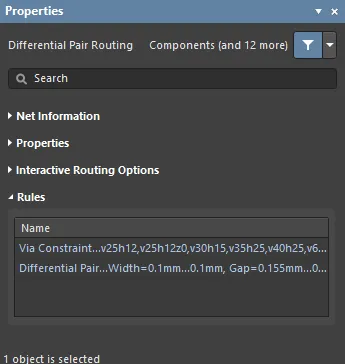
Constraints defined by the applicable design rules will be listed under the Rules section of the Properties panel.
- Via Constraint – click to open the Edit PCB Rule dialog in which you can define PCB rules for via.
- Differential Pair Constraint – click to open the Edit PCB Rule dialog in which you can define PCB rules for the differential pair.
Improving the Quality of the Routing
Main article: Glossing & Retracing of Existing Routes
The PCB editor includes powerful tools for improving the quality of existing routing. These tools are known as Glossing and Retracing and both are available in the Route menu.
- Gloss - focuses on improving the trace geometry, attempting to reduce the number of corners and shorten the overall route length. Gloss preserves the existing trace width and differential pair gap. Glossing respects the current Gloss Effort (Routed) setting configured in the PCB - Interactive Routing page of the Preferences dialog (show image
![]() ).
).
- Retrace - assumes the overall geometry is satisfactory, focusing instead on verifying that the routing meets the design rules. Where Gloss preserves the existing trace width and pair gap, Retrace changes them to Preferred. Retrace is an excellent tool to use when a Differential Pair Routing design rule has changed, and that change needs to be applied to existing routing.
The animation in the previous section, Routing a Differential Pair, includes a simple demonstration of glossing with the Gloss Effort (Routed) set to Strong.
Interactively Modifying the Differential Pair Routing
Main article: Modifying Existing Routes
During routing there will be many instances where you need to change some of the existing routing, for example, you might not be happy with the pad exits and you want to re-shape them (as shown in the video below). While you can change the existing routing using a drafting type approach of clicking and dragging track segments, it is often easier to simply re-route.
To do this, select the Route » Interactive Differential Pair Routing command, then click anywhere on the existing routing. Proceed to route the new path, coming back to meet the existing routing where required. This will create a loop between the old path and the new path. When you right-click or press Esc to terminate the route, the redundant segments are automatically removed, including any redundant vias.
The loop removal feature is employed by enabling the
Automatically Remove Loops option - either from within the
Properties panel (while in interactive differential pair routing mode), or on the
PCB Editor - Interactive Routing page of the
Preferences dialog. To toggle this feature on or off while routing, use the
Shift+D keyboard shortcut.
Differential pair routing is slightly different from single net routing. Single net routing can be configured so that the last segment is hollow (the look-ahead segment); this segment is not placed when you click. Differential pair routing does not include look-ahead segments, so when you click you will place all visible segments. Position the cursor to ensure that there are no redundant segments.
If you are adjusting differential pairs by manually dragging track segments, you can either push one pair member with the other or drag each independently.
Use the loop removal feature to interactively re-route a diff pair along a new path, the old routing loop is automatically removed. Pairs can also be modified by dragging one route so that it pushes the other.
Interactive Via Dragging
PCB designers can spend a lot of time adjusting the routing, perhaps due to a late design change, or to achieve completion of their design. This can mean pushing and shoving existing routing, dragging vias, and nudging components.
 Adjust the via dragging behavior in the Properties panel.
Complimenting the support for glossing of neighbor routes, via dragging is also supported. Via dragging supports Neighbor Glossing, configured through the Interactive Via Dragging mode of the PCB editor's Properties panel. Press Tab during via dragging to access the panel and adjust the settings.
Differential Pair Dragging
To recognize the members in a differential pair, the concept of Coupling is used. When the software recognizes objects that belong to a differential pair it will attempt to drag the pair's partner track or via if the Keep Coupled option is enabled in the Interactive Sliding or the Interactive Via Dragging modes of the Properties panel.
Press X as you drag a via-pair to rotate the pair by 90 degrees.
To confirm that the partner objects are coupled, the software checks that the objects:
- For via pairs - belong to the pair, and are closer than
2 * Preferred Gap
- For track pairs - belong to the pair, are on the same layer, are separated by no more than the
Preferred Gap
Displaying the Available Clearance
Have you ever been stuck during routing, wondering why the route won't fit through that gap? This frustration is even more likely during differential pair routing. Altium Designer includes a feature to help with this, called dynamic display of clearance boundaries. When enabled, the no-go clearance area defined by the existing objects + the applicable clearance rule is displayed as shaded polygons within a local viewing circle, as shown in the video below. Press Ctrl+W to toggle the feature on and off.
 Dynamically display the clearance boundaries during differential pair routing.
The display area can be restricted to a region around the current cursor location, or it can be the entire screen. This is controlled by the Reduce Clearance Display Area sub-option on the PCB Editor - Interactive Routing page of the Preferences dialog.
The Quick Differential Pair Routing Tool
The Quick Differential Pair Routing command (accessed from the main menu and the Active Bar) offers lighter routing with less settings and capabilities, suitable for simpler designs. Its general behavior and shortcuts is the same as the standard Interactive Differential Pair Routing command.

Capabilities include:
- A number of routing modes, such as: stop at first obstacle, walkaround, and push and shove.
- Powerful dragging capabilities that maintain track angles and orthogonality.
- A loop removal feature that makes re-routing a quick and easy process.
The Quick Differential Pair Routing tool helps maximize routing efficiency and flexibility in an intuitive way, including following cursor path for laying route sections, single-click routing completion, pushing or walking around obstacles, and automatically following existing connections, all in accordance with applicable design rules.
This router is referred to as Quick because it offers a reduced feature-set. Features that are not included in the Quick Differential Pair Router include:
- No turn smoothing
- Little support for Any Angle routing
- No pushing of T-junctions
- Simple Push&Shove support
- No Miter Ratio, Min Arc, or Pad Entry Stability
- Simple Gloss Effort, with no support for Gloss Neighbor
- No differential pair convergence when exiting the start pins laterally
- No hugging by routed differential pairs
- No differential pair maintenance when a neighbor differential pair is pushed
If you need any of these features, use the Interactive Differential Pair Routing tool.
The following collapsible sections contain information about the Quick Differential Pair Routing options and controls available:
To recognize the members in a differential pair, the concept of Coupling is used. When the software recognizes objects that belong to a differential pair it will attempt to drag the pair's partner track or via if the Keep Coupled option is enabled in the Interactive Sliding or the Interactive Via Dragging modes of the Properties panel.
Net Information

- DP Name – displays the differential pair name.
- DP Class – displays the differential pair class that the routing belongs to (if it is a member of a differential pair class).
- Selected
- Length – the total length sum of the selected segments.
- Delay – the total delay of the selected segments, including those unrouted.
- Total
- Length – the total Signal Length. The Signal Length is the accurate calculation of the total node-to-node distance. Placed objects are analyzed to resolve stacked or overlapping objects and wandering paths within pads, and via lengths are included. If the net is not completely routed, the Manhattan (X + Y) length of the connection line is also included.
- Delay – the delay of the routed segments of the Total Length.
Select the clickable links of the
DP Name,
DP Class,
Length, and
Delay from the
Differential Pair Routing mode of the
Properties panel to be redirected to the
PCB – Nets panel, where you may view and change details of the nets associated.
Properties

- Layer – use the drop-down to specify on which layer the routing is located.
- Gap – use the drop-down or the Shift+6 shortcut to cycle through the permissible clearances.
- Min – select to specify the minimum permissible clearance between primitives on different nets within the same differential pair.
- Preferred – select to specify the preferred clearance between primitives on different nets within the same differential pair.
- Max – select to specify the maximum permissible clearance between primitives on different nets within the same differential pair.
- Via – if the via is associated with a template, the template name is displayed here.
- Via Diameter – specify the via diameter.
- Via Hole Size – specify the via hole size.
- Width – use the drop-down to specify the width.
- Min – signifies that the design rule minimum width defined for the current net will be used
- Preferred – signifies that the design rule preferred width defined for the current net will be used.
- Max – signifies that the design rule maximum width defined for the current net will be used.
Interactive Routing Options
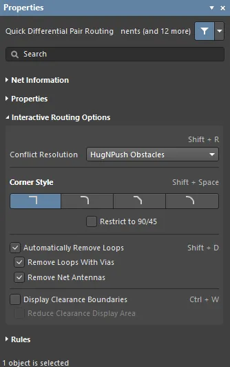
- Routing Mode – use the drop-down or use the Shift+R shortcut to cycle through the desired routing modes. The following choices are available:
Ignore Obstacles – select to ignore existing objects (routing can be freely placed). Violations are highlighted.Walkaround Obstacles – select to have the Interactive Router route around existing tracks, pads and vias. If this mode cannot walk around an obstacle without causing a violation, an indicator appears to show that the route is blocked.Push Obstacles – select to have the Interactive Router move existing tracks out of the way. This mode can also push vias to make way for the new routing. If this mode cannot push an obstacle without causing a violation, an indicator appears to show that the route is blocked.HugNPush Obstacles – select to have the Interactive Router hug existing tracks, pads, and vias as closely as possible and where necessary, push obstacles to continue the route. If this mode cannot hug or push an obstacle without causing a violation, an indicator appears to show that the route is blocked.Stop At First Obstacle – in this mode, the routing engine will stop at the first obstacle that gets in the way.AutoRoute Current Layer – select to enable auto-routing only on the current layer.AutoRoute MultiLayer – select to enable auto-routing on multiple layers.
- Corner Style – select the desired routing corner style or use the Shift+Spacebar shortcut to cycle through the corner styles.
- Restrict to 90/45 – enable to restrict the routing to 90 degrees and 45 degrees only.
- Automatically Remove Loops – enable to automatically remove any redundant loops that are created during manual routing. This allows you to re-route a connection without having to manually remove redundant tracks. However, there are times when you need to route nets, such as power nets and when you need loops; you can toggle this option for a selected net by using the Shift+D shortcut to override this global setting for the same net.
- Remove Loops With Vias – enable to automatically remove loops with vias. Disable this option for vias to remain during loop removal.
- Remove Net Antennas – enable this option to remove any track or arc end that is not connected to any other primitive and forms an antenna.
- Display Clearance Boundaries – enable this option to have the no-go clearance area defined by the existing objects and the applicable clearance rule displayed as shaded polygons within a local viewing circle. This option is not available in the Ignore Obstacles routing mode.
- Reduce Clearance Display Area – enable this option to use a smaller clearance boundary. This option is available only when the Display Clearance Boundaries option is enabled.
Rules
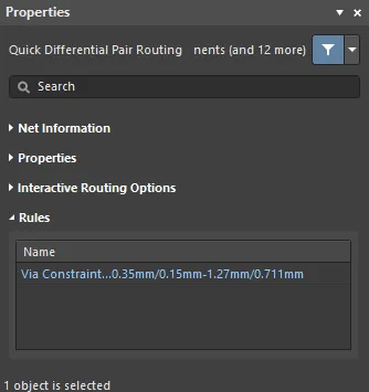
Constraints defined by the applicable design rules will be listed under the Rules section of the Properties panel.
- Via Constraint – click to open the Edit PCB Rule dialog in which you can define PCB rules for a via.
- Differential Pair Constraint – click to open the Edit PCB Rule dialog in which you can define PCB rules for the differential pair.
Matching the Lengths of Differential Pairs
Differential pairs are often used in high-speed designs due to their inherent immunity to noise, and the fact that they simplify the challenge of providing a high-quality return path for the signals. However, like single-sided signals, their lengths must be managed to ensure the signal timing requirements are met.
During differential pair routing, the length of each of the two nets in the pair is displayed on the Status bar, and also in the Heads-up display (Shift+H to toggle on/off). The length values displayed in the PCB panel are updated when you drop out of routing a pair.
 The current route length of each net in the pair is displayed in the Heads-up display (Shift+H to toggle on/off).
The PCB panel is used to examine objects in the design space and includes modes for examining Nets, Differential Pairs and xSignals, amongst others. The panel includes details about each net/differential pair/xSignal, including the signal length and the delay - right-click in each section of the panel to display a context menu of commands for that section. For example, when the panel is in Nets mode, right-click in the Nets section of the panel and use the Columns sub-menu to enable or disable details such as Signal Length and Delay. When there are Length and/or Matched Length rules applied, the Signal Length column for nets that fail the design rule will highlight in orange (less than target length) or red (exceeds target length).
 Use the PCB panel to monitor the progress of length matching.
► Learn more about the PCB panel
Matched Length and Length Design Rules
Length and Matched Length design rules can be defined to ensure that the flight time and skew timing requirements are met. As well as being used during a design rule check (DRC), these rules are also used during interactive length tuning.
The Matched Length design rule detects the longest pair targeted by the rule scope and uses the Average Length value of that pair as the reference to compare the other targeted pairs, requiring their lengths to be within + or - the Tolerance defined in the rule. The Average Length value is shown in the Differential Pairs Editor mode of the PCB panel.
Length and Matched Length design rules can be scoped by Length Units or Delay Units. If the rules are scoped by delay, the Length Tuning Gauge will also display using delay.
Within-Pair and Between Pair Design Rules
It is likely that you will have matched length requirements between the pairs, and also within each pair.
To manage this, create suitable Matched Length design rules:
- Define a Matched Length design rule that applies across (between) the pairs (achieved by selecting the Group Matched Lengths option). Scope the rule to apply to the required pairs (or xSignals), as shown in the image below.
 Create a matched length rule to define the length requirements between the differential pairs, or in this example, between the xSignals.
- Define another Matched Length design rule that applies within the pair (achieved by selecting the Within Differential Pair Length option). This rule ensures the lengths of the two nets within each pair are within tolerance. Note that this rule must be scoped using a Where the Object Matches setting that targets differential pairs, as shown below. This rule should have a higher priority than the between-pairs rule.
 Create a second matched length rule to define the length requirements within the pairs.
Length Tuning a Differential Pair
Main article: Length Tuning
The length of pairs, and the nets within each pair, are tuned using the two length tuning commands. To tune the lengths:
- The length of a differential pair can be accurately tuned using the Interactive Diff Pair Length Tuning command on the Route menu. During length tuning, you can use shortcuts to interactively adjust the accordion style and size, or press Tab to open the Properties panel in Differential Pair Length Tuning mode. In the panel, the target length is defined:
-
From the applicable Length and/or Matched Length design rules
-
From a user-selected routed diff pair
-
Manually, enter the value in the Target Length field

- To tune a net within a pair, use the Interactive Length Tuning command on the Route menu. If you attempt to tune the longer net in the pair, the message Target Length Shorter than Old Length will appear.
 Tune the lengths of differential pairs first, then tune the length of the shorter net within a pair.
If you do not get tuning accordions appearing during length tuning it is most likely that the current settings are not suitable for the space available to place an accordion. If this occurs during tuning, press Tab to open the Properties panel in Differential Pair Length Tuning mode and check that the settings in the Pattern section of the panel are sensible. For example:
- The Max Amplitude value may be too large
- When the Style is Mitered Arcs, the Miter percentage may be too great to form an arc for the current Amplitude and Space
A good option is to set the Style to Mitered Lines, click the Pause button to resume length tuning then use the 1 & 2 shortcuts to interactively adjust the Miter, the 3 & 4 shortcuts to adjust the Space (pitch), and the , and & . shortcuts to adjust the Amplitude. When the tuning is looking how you want it, press the Spacebar to cycle to your preferred Style.
Refer to the Length Tuning page to learn more, where you will find a detailed list of the shortcuts that can be used to change the accordion style, amplitude and pitch. The page also explains how the software decides which rule settings to obey when there are overlapping settings in the Length and Matched Length design rules.
Demonstration of Length Tuning and Modifying the Accordions
The video shows pair lengths being tuned against other pairs (based on xSignal lengths) by adding length tuning accordions. The shorter member of each pair is then length-tuned against the longer member of that pair. The video then shows how pairs can be moved and reshaped interactively, how a tuning accordion can be deleted, and how a new accordion can be shaped during placement using shortcuts.
The length of a differential pair can be tuned by adding length tuning accordions. The accordion is an object that can be moved, reshaped and deleted.
See Also