Multi-Circuit Board Design Rules: Designing PCBs for Interconnected Systems in Altium Designer

Mini commercial products do not have just a few PCBs; they use multiple PCBs in a single enclosure to create a product. Most easy design software does not fully accommodate multi-board PCB design, but it is a powerful approach that helps verify connectivity across an entire board stack. The overall workflow for multi-board design starts with schematics and completes the remaining electrical design, followed by the preparation of manufacturing and assembly deliverables.
Multi-board PCB design also requires a close interface with a mechanical designer to ensure form, fit, and function in an enclosure. Many designs take the approach of defining mechanical constraints and building the PCB within the enclosure. When this is the case, careful placement of connectors and verification of net connectivity across multiple PCBs make the difference between a successful product launch and a failed design.
Mechanically Driven or Electrically Driven Multi-Board PCB Design?
Multi-board PCB systems design can be driven mechanically or electrically. One side must set up the constraints for the other, which is required to ensure that the multi-board assembly fits within an enclosure. Either the mechanical designer sets constraints through the enclosure first, or the electrical designer is free to design the board, and the mechanical designer works around the PCB outlines. Either approach is appropriate for a multi-board system and for single-board PCBs in general.
Once the approach is determined, there will need to be a back-and-forth transfer of design data between the electrical designer and the mechanical designer. Bidirectional collaboration between PCB design software and MCAD software is possible with today's cloud data management platforms, like Altium 365. Users of popular MCAD applications can pull the PCB layout into their software and work on all the mechanical elements that go into the final product. They can also push mechanical changes back to the PCB designer as required. The back-and-forth process implemented here ensures design data can be quickly and efficiently sent between engineering teams with ease.
This covers the process of creating the product design, but what about implementing connectivity? The connectivity question requires designers to consider several options between the PCBs and their multi-board assembly.
Physical Connectivity in a Multi-Board System
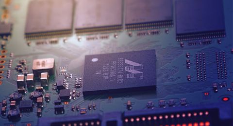
The entire reason we have multiple PCBs in a multi-board system is to have different electrical components in different locations, and this requires transferring signal and power across some interconnect between PCBs. There are several options for doing this, which will then determine the form factor and reliability of the completed assembly.

Intuitive Multi-Board System Design
The easiest way to create complex designs and error-free system interconnections.
- Board-to-board connectors
- Through-hole or pin connectors
- Flexible printed circuit cables
- Standardized ribbon cables or wired cables
- Custom cable assemblies
- Floating wires soldered to posts or plated through holes
- Edge contact pins and slot connectors
These components provide the core electrical connectivity and power transfer between PCBs in the assembly. They also play an important role in EMC, as they can be sources of radiated emission or have high susceptibility, depending on how the interconnect is constructed. It's not just about choosing the type of connector or part number; it's also about designing the pinout and understanding the grounding strategy between the boards in the system.
Power Handling
A key capability of some boards in a multi-board assembly is supplying power, which means a connector and cable assembly will be needed to handle the required amount of power. Connector manufacturers market their products as suitable for power, signal, or both, so the designer should check their specifications to ensure a selected connector can provide the required amount of power. Relevant specifications include:
- Current per pin or per circuit
- Isolation voltage between pins
- Flash or breakdown voltage
- Maximum temperature limit or excursion
As long as power is not too high, it is possible to consolidate power and signal routing into a single interconnect. It's also possible to have a single board supply power to multiple peripheral boards using a custom harness rather than daisy-chaining boards together with individual power cables. This is usually done with a board interface, which is always custom-designed and often hand-wired into a custom harness.

Power supplies are one of the most common elements in a multiboard system that uses a harness to connect to other PCBs.
Easy, Powerful, Modern
The world’s most trusted PCB design system.
Signal Integrity in Multi-Board Interconnects
Interconnects between boards that carry signals should ensure signals are not degraded while traveling between the two ends of the interconnect. Multi-board signal integrity is related to multi-board grounding and defining pinouts in a multi-board system. Following some of the same rules we apply for high-speed digital design will help ensure signal integrity across a multi-board interconnect.
Depending on the interface and connector, pinouts for some interconnects are standardized, and the designer will not have the freedom to change this. For example, consider Ethernet: this interface has a standard set of signals that are used to ensure compatibility with off-the-shelf Ethernet cables. Therefore, unless you are designing a custom cable assembly, pinouts should be set in the PCB based on the interface standard. However, other modules or boards in a system give you full freedom to select the pinout and a connector.
When selecting a connector and designing the pinout, there are several specs that should be examined:
- Pin size and pitch, which will determine how signals can route into the connector
- Total number of ground pins that can be allocated as signal references
- Connection style (board-to-board or board-to-wire/cable)
- Connector data rate or bandwidth rating
- Availability of ground or chassis connections for use with shielded cabling
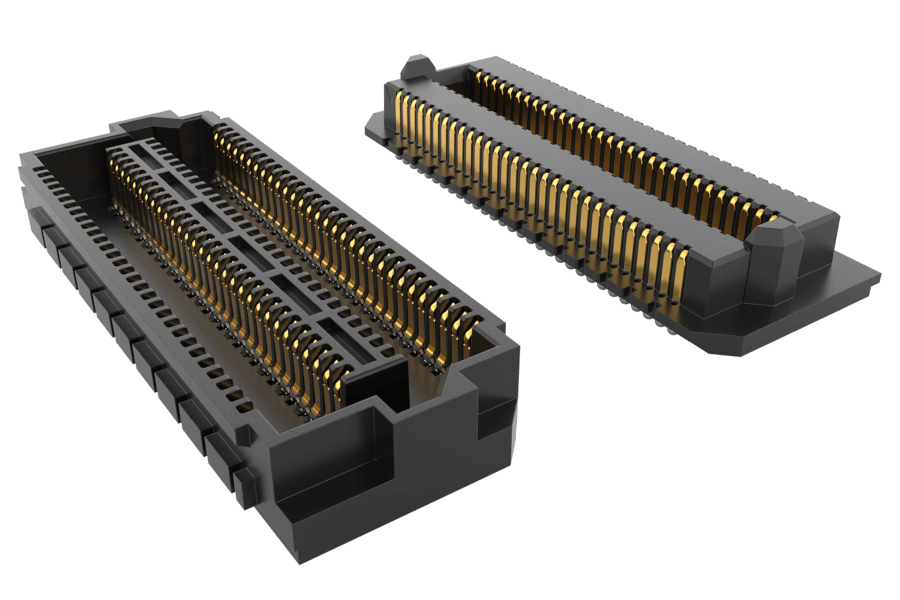
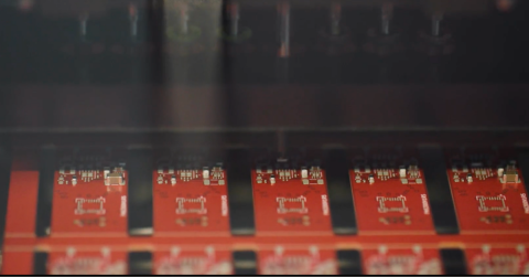
For board-to-board connections involving high-speed data transfer, higher data rates tend to require physically smaller board connectors, such as the SMD options from Samtec shown below. These also require interleaving ground pins in between signal pins so that a reference plane connection is carried across the interconnect.
Layer Stackup Design
Implement any kind of layer stack for both rigid and rigid-flex PCBs.
Example high-density board-to-board connectors (0.635 mm pitch) that can support high-speed signal propagation. Image credit: Samtec.
On each PCB, routing into the connectors must still follow best practices for high-data-rate digital channels. The connector itself will also only provide bandwidth up to a certain high-frequency limit. This will limit the maximum data rate per pin or interface.
EMI and Grounding
These two areas of multi-board design are related to each other, as failure to properly ground circuits or account for grounds across a pair of PCBs can lead to emissions failures. There’s also the matter of filtering and shielding between boards and with respect to the enclosure, both of which can be a last-minute solution to solving an EMI problem.
While there are no specific standards regarding EMI for multi-board assemblies, there are some simple steps designers can take to ensure EMC in a multi-board assembly. EMC is a system-level challenge with different requirements in different industries or applications, and there are many components, circuits, and design approaches that can be used to ensure EMC:
- Placement of chokes and/or filters on interconnects
- Prioritizing differential interfaces for board-to-board communication
- Eliminating floating grounds by bridging ground across interconnects
- Ensuring correct chassis connections on all boards in the system
- Filtering on power lines across board-to-board interconnects
The filters and chokes used for signal lines must be carefully chosen, or they must be selected based on the interface standard where they will be used. Because common noise is the dominant radiated EMI failure mechanism, common-mode chokes are often used at cable interfaces. Some chokes are designed and qualified specifically to support high-speed serial interface standards, such as HDMI or USB. For power, a higher-order filter circuit providing both common-mode and differential-mode filtering needs to be custom-designed based on the load where power will be delivered.
PCB Layout
An integrated PCB editor along with real-time connection to multiple domains.
The Role of Harness Design
Although board-to-board connectors for high-speed interfaces get a lot of attention, many products will use custom cabling and custom wire harnesses. As more PCBs are added into a multi-board assembly, it eventually becomes impossible to connect everything with board-to-board connectors. Designers will usually choose a rigid-flex assembly or a custom wiring harness. This is why access to a logical harness design tool can be very helpful for design teams.
Harness design is quite useful for routing power and signal in a multi-board assembly, but the designer will need to create documentation and instructions related to the construction and installation of the harness. Just like PCBs in a multi-board system, harness design is both logical, with schematics, and there is a graphical component showing the wiring path for the harness.

Physical and logical design of a custom wiring harness assembly in Altium Designer.
Wiring harnesses also need some basic manufacturing documentation. This should be included in the mechanical drawing of the harness. For example, wiring harness documentation should include:
Where the World Designs Electronics
Break down silos and enhance collaboration across all aspects of electronics development
- Wire gauge and core type
- Sheathing material and color for each wire
- Part number in each branch of the harness
- Assembly process details
- Pin or crimp part numbers, if applicable
Wiring harnesses do not always produce the most compact results, and they tend to be used more often in systems requiring moderate to high power transmission between PCBs. There are more elaborate solutions for connecting boards, which essentially function the same as a wire harness, such as an FPC with surface-mount or board connectors.
Your Design Tools Must Lead the Way
Multi-board designs are at risk of interconnect errors and even mechanical errors with simpler PCB design software packages. Dedicated multi-board design tools help design teams match physical interconnects to logical definitions in the schematics. This means design rule checks can extend up to the level of board-to-board interconnects and help ensure multi-board assemblies always have the correct connection definitions and fit in a mechanical enclosure.
The built-in multi-board PCB systems design features in Altium Designer® bring the industry's best PCB layout and verification features into a multi-circuit board workflow. When you’re ready to collaborate with your mechanical designer to verify and analyze the completed design, the MCAD CoDesigner app in Altium 365 enables bi-directional collaboration, unlike any other design environment. Everything you need to design and produce advanced electronics can be found in one software package.
We have only scratched the surface of what is possible to do with Altium Designer on Altium 365. Start your free trial of Altium Designer + Altium 365 today.

About Author
Related Resources


Related Technical Documentation

Table of Contents
- Mechanically Driven or Electrically Driven Multi-Board PCB Design?
- Physical Connectivity in a Multi-Board System
- Power Handling
- Signal Integrity in Multi-Board Interconnects
- EMI and Grounding
- The Role of Harness Design
- Your Design Tools Must Lead the Way
Take advantage of the world's
most trusted PCB design system.
One interface. One data
model. Endless possibilities.
Effortlessly collaborate with
mechanical designers.
The world's most trusted
PCB design platform
Best in class interactive
routing
View License Options
Thank you, you are now subscribed to updates.
