In order to run a successful Signal Integrity analysis of the design and obtain accurate results, the following has to be performed before running the analysis.
-
Although each net can be screened to provide net and impedance data, not all nets can be analyzed for signal integrity characteristics (voltage and timing). In order to screen successfully for all characteristics, a net must contain at least one IC with an output pin and no other components. Resistors, capacitors and inductors for example will not provide simulation results on their own because of their lack of output pin to provide a driving source. It should be noted that when bidirectional nets are screened, both directions are simulated and the worst case result is displayed.
-
The associated Signal Integrity model type for each component has to be correct. This is achieved via the Signal Integrity Model Assignments dialog or by manually setting the correct entry for the Type field in the Signal Integrity Model dialog, when editing the Signal Integrity model associated to the component placed on the schematic source document. If this entry is not defined, the Signal Integrity Model Assignments dialog will attempt to guess the type of the component based on its characteristics. If this entry is not defined, the type Integrated Circuit will be assumed. For more information, see Adding SI Models Using the Signal Integrity Model Assignments Dialog.
-
There must be Supply Nets design rules. Generally, there should be at least two rules, one for power nets and one for ground nets. The scope for these can be either net or net class. Supply nets cannot be analyzed in Signal Integrity. For more information, see Signal Integrity Design Rules in Schematic or Signal Integrity Design Rules in PCB.
-
A Signal Stimulus design rule may be set up. You only need a stimulus rule if you want to override the default stimulus, so this is generally not required.
-
The layer stack for the PCB must be set up correctly. The Signal Integrity Analyzer requires continuous power planes. Split planes are not supported, so the net that is assigned to the plane is used. If they are not present, they are assumed, so it is far better to add them and set them up appropriately. The thickness of all layers, cores and prepreg must also be set correctly for the board. Use the Design » Layer Stack Manager command to set up the layer stack in the PCB editor. When running Signal Integrity in the schematic only mode, a default two layer board with two internal planes is used. You could create a blank PCB with a layer stack set up if more control was required. Refer to the Defining the Layer Stack page to learn more.
The characteristics of a signal, such as the voltage level, are determined by the model assigned to the output pin in the net under test. Pin models are assigned as part of the component model assignment process, and these component-level model assignments can be retained by updating the schematic. An individual pin model can also be overridden, for example, by double-clicking on a pin in the Signal Integrity panel – note that these pin-level reassignments are not retained between editing sessions.
Adding SI Models Using the Signal Integrity Model Assignments Dialog
The simplest way to add signal integrity models to your design is to use the Signal Integrity Model Assignments dialog.
-
Select Tools » Signal Integrity from the menus. If you are just starting signal integrity on a project and there are components which do not have signal integrity models attached, you will be prompted by the Errors or warnings found dialog to set up the model assignments using the Signal Integrity Model Assignments dialog.
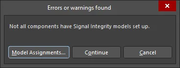
The Errors or warnings found dialog
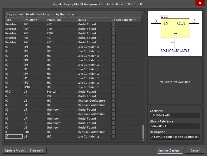
The Signal Integrity Model Assignments dialog
Alternatively, if you have clicked Continue and the Signal Integrity panel is visible, it is possible to enter the Signal Integrity Model Assignments dialog at any time by clicking the Model Assignments button in the panel. Note that doing so will cause all results to be cleared and recalculated since any changes to model assignments invalidate any existing results.
If models have been already set up for all components, the SI Setup Options dialog will display. See Configuring the SI Setup Options for more information.
-
If you click on Model Assignments in the Errors or warnings found dialog, the Signal Integrity Model Assignments dialog displays.
When run, the Signal Integrity Models Assignment dialog attempts to make educated guesses as to the necessary signal integrity model required for each component that does not contain a signal integrity model. All components, including those with models already defined (and the model information) will be displayed in the Signal Integrity Models Assignment dialog. Each component will be assigned a status as described in the following table.
| Status |
Definition |
| No match |
The Signal Integrity Model Assignments dialog was unable to find any characteristics linking this component to a particular type. It will likely need modification from the user to be set up correctly. |
| Low confidence |
The Signal Integrity Model Assignments dialog has selected a type for this component, but there was not strong evidence. |
| Medium confidence |
The Signal Integrity Model Assignments dialog has selected a type for this component and has reasonable confidence for the guess. |
| High confidence |
The Signal Integrity Model Assignments dialog has selected a type for this component and it fits most of the characteristics usually associated with this type of component. |
| Model found |
An existing model was found for this component. |
| User modified |
A component will change to this status once the user has modified it from the Signal Integrity Model Assignments dialog's initial guess. |
| Model added |
This status is used when the user has used the Signal Integrity Model Assignments dialog to modify the schematic document to save the new model. |
Modifying Component Models using the Signal Integrity Model Assignments Dialog
-
Select the component that you want to modify its model.
-
Select the correct type. There are seven types of components for Signal Integrity – resistor, capacitor, inductor, diode, BJT, connector, and IC. The type of each component can be selected via a drop-down in the Type column or via the right-click menu.
-
Set the value for a resistor, capacitor or inductor. If possible, the Signal Integrity Model Assignments dialog will attempt to place the correct value for the component in this column based on the comment field and parameters on the component. If this requires modification (or is not present), this should be done at this point. The special case of part arrays (such as resistor arrays) is done via a separate dialog accessed by clicking in the column (see Manually Adding Signal Integrity Models to Components for more details).
-
If the component is an IC, the choice of technology type is important as this will determine the characteristics of the pin models used in the analysis. This can be selected via the drop-down list in the Value/Type column or accessed through the right-click menu (Change Technology).
-
Finally, it may be necessary to specify more detail than allowed in the Signal Integrity Model Assignments dialog, such as for IBIS models. This can be achieved by selecting Advanced from the right-click menu. See Manually Adding Signal Integrity Models to Components for more details on this process.
Saving Models
Once models have been chosen for any or all of the components, the schematic documents can be updated to permanently store this information.
-
Check the Update Schematic column in the Signal Integrity Model Assignments dialog for all components that are to be updated. Then click the Update Models in Schematic button.
-
All new Signal Integrity models (or modified existing ones) for each selected component will be added to the schematic documents. The schematic documents will need to be saved later.
It is not necessary to save models to proceed with the Signal Integrity analysis process. If models are not saved, the analysis will proceed with all models configured as they are currently shown in the Signal Integrity Model Assignments dialog. However, the next time the Signal Integrity tool is used, any changes will have been lost.
Manually Adding Signal Integrity Models to Components
To add a Signal Integrity model to a schematic component:
-
For a placed component in the schematic editor – select the component and open the Properties panel.
-
For a component being edited in the schematic symbol editor – make the required component active by selecting its entry in the SCH Library panel and open the Properties panel.
Click the Add button in the Parameters region of the Properties panel and select Signal Integrity. The Signal Integrity Model dialog will open.

Set up your model and click OK.
Setting Up Passive Components
When setting up parts such as resistors and capacitors, it is usually sufficient to enter a type and a value. The value can be entered in the Value field and can be set as a parameter for the whole component.
There is also support for components like resistor arrays. This can be achieved by, after selecting the component type, clicking the Setup Part Array button in the Signal Integrity Model dialog. The Part Array Editor dialog allows the connections between pins and the value/model for those connections to be configured.
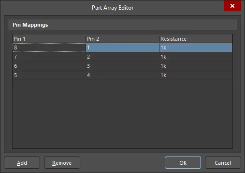
The Part Array Editor dialog
Setting Up an IC
There are several alternatives when setting up an IC type model.
-
After selecting the type (IC), it is sufficient to select a technology type. This will ensure that when simulating this component, the appropriate pin models for that technology will be used. The full list of available technologies is in the collapsible section below.
Available Technology Types
| Technology Type |
Description |
| ABT |
Advanced Bipolar CMOS Technology |
| AC |
Advanced CMOS |
| ACT |
Advanced CMOS with TTL inputs |
| AHC |
Advanced High Speed CMOS |
| AHC_50 |
Advanced High Speed CMOS 5.0V |
| AHCT |
Advanced High Speed CMOS with TTL inputs |
| AHCT_50 |
Advanced High Speed CMOS 5.0V with TTL inputs |
| ALS |
Advanced Low Power Schottky |
| ALVC |
Advanced Low Voltage CMOS |
| AS |
Advanced Schottky |
| BCT |
Bipolar CMOS Technology |
| BTL |
Backplane Transceiver Logic/Futurebus+ |
| CMOS |
CMOS |
| F |
FAST |
| FCT |
FAST CMOS Technology |
| GTL |
Gunning Transceiver Logic |
| GTL_LVT |
Gunning Transceiver Logic Low Voltage |
| HC |
High Speed CMOS |
| HCT |
High Speed CMOS with TTL inputs |
| HLL |
High Speed Low Power Low Voltage CMOS |
| LS |
Low Power Schottky |
| LV |
Low Voltage High Speed CMOS |
| LVC |
Low Voltage CMOS |
| LVT |
Low Voltage BiCMOS Technology |
| S |
Schottky |
| STD_TTL |
Standard TTL |
| TTL |
TTL |
-
If more control is required, it is possible to assign specific technologies or pin models to individual pins. This can be done by selecting from the drop-down lists for the pins in the pin list at the bottom of the Signal Integrity Model dialog. Note that any changes here will override the base technology for the component.
Importing IBIS Files
Another important option is the ability to import IBIS files.
-
To use an IBIS (Input/Output Buffer Information) file to specify an IC model's input and output characteristics, click the Import IBIS button in the Signal Integrity Model dialog. Select the IBIS file from the Open IBIS File dialog and click Open. The IBIS Converter dialog displays.
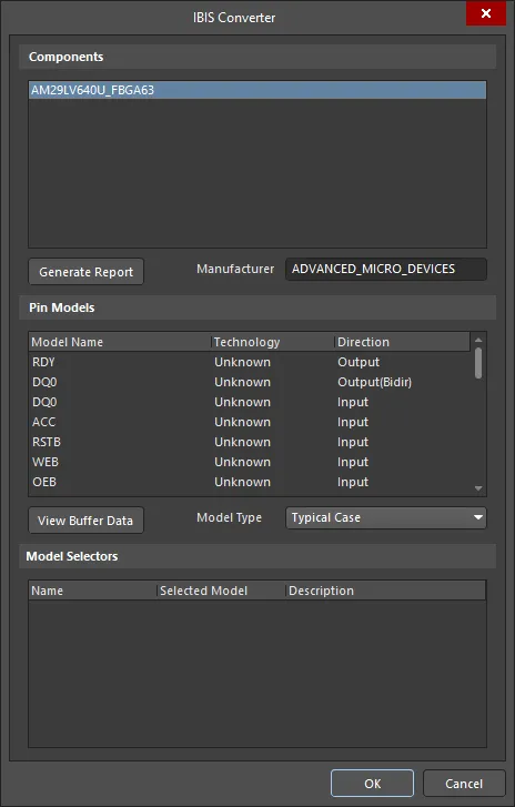
The IBIS Converter dialog
-
Select the required component contained in the IBIS file. Altium Designer will read the IBIS file and import the pin models from the IBIS file into the library of installed pin models. If a duplicate model is found, you will be asked if you wish to override the existing model. Additionally, all pins on the component will have the appropriate pin model assigned as specified in the IBIS file.
-
A report will automatically be generated stating which pins were successfully and unsuccessfully assigned. Further customization is possible by manually selecting the models for the appropriate pins as described above.
-
Click OK to complete importing the IBIS information and return to the Signal Integrity Model dialog.
Editing Pin Models
It is possible to add or edit an existing pin model by specifying various electrical characteristics of that pin. Note that this is also available for other types such as BJTs, Connectors and Diodes.
-
To modify pin models, click the Add/Edit Model button in the Signal Integrity Model dialog if this button is available for that type. The Pin Model Editor dialog displays.
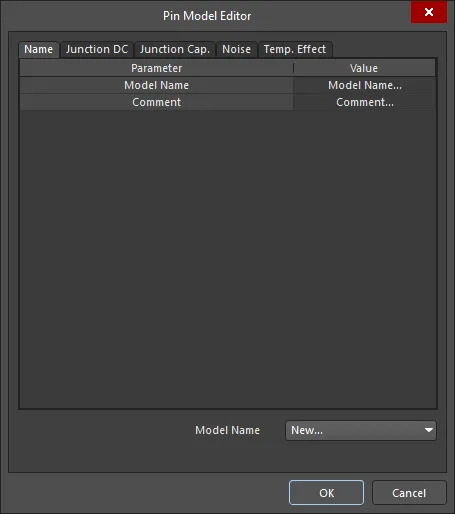
The Pin Model Editor dialog
-
Click on New in the drop-down list for the Model Name.
-
Make the necessary changes and click OK.
-
If this is a new pin model, that model will now be available for selecting on the pins in this (and other) components.
Working with the Ibis Model Implementation Editor
To support third party tools that require dedicated IBIS models for their Signal Integrity simulations and cannot use Altium Designer's own Signal Integrity model format (referred to as SI Macro Models), Altium Designer incorporates a dedicated IBIS model implementation editor, allowing the IBIS model to be attached to the schematic component. So you can either:
-
Import the IBIS pin models into the component pins during Signal Integrity Analysis (to be stored as Altium Designer SI Macro Models) as described above (see Importing IBIS Files), or
-
Attach the IBIS model to the schematic component, as described below.
This feature supports all versions of IBIS model specification, up to and including version 4.0.
To add an IBIS model to a schematic component:
-
For a placed component in the schematic editor – select the component and open the Properties panel.
-
For a component being edited in the schematic symbol editor – make the required component active by selecting its entry in the SCH Library panel and open the Properties panel.
Click the Add button in the Parameters region of the Properties panel and select Ibis Model. The IBIS Model dialog will open.

Any number of IBIS model links can be defined for a schematic component, but only one can be the active model at any given time.
IBIS Model
Specify the name for the model – exactly as it appears within the .ibs file – and give the model link a meaningful name, perhaps describing what the implementation in this domain represents.
Alternatively, and especially if you are unsure of the name, use the Browse button to access the Browse Libraries dialog. Use this dialog to browse IBIS model files across all currently available libraries. Use the Find feature in this dialog if the required model files are not part of the currently available libraries.
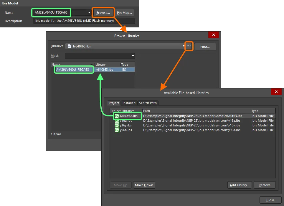
Specify the name of the model directly, or browse for it.
When browsing for an IBIS file, the Name drop-down will present all models, by name, defined within that file. Simply select the required one.
The mapping of schematic component pins to IBIS model pins is defined in the Model Map dialog, accessed by clicking the Pin Map button.
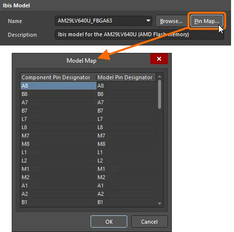
Verify component-to-model pin mapping in the Model Map dialog.
IBIS File Location
Options are available in this region of the IBIS Model dialog with which to specify how the software is to locate the model – provided the model name is defined:
-
Any – all Available Libraries (project libraries, installed libraries and libraries found along defined search paths) are used to look for the model.
-
File name – enter the full file name in which the model resides (e.g.,
lv640f63.ibs). All Available Libraries are used to look for the model. If not found here, the default library path (the Library Path field on the System – Default Locations page of the Preferences dialog) will be interrogated to see if the named file can be found there.
-
File path – enter the full path/name of the file. Click the Choose button to browse to the file. This option will always find the model, since it is explicit (provided of course the file remains in that directory!).
-
Integrated/Database Library – post-placement, if the component is placed from an integrated or database library, the model can be sourced directly from that same library, provided the library is part of the Available Libraries set.
If successfully located, indication of where the model was found will be presented.

Specify how to find the IBIS model.
Pin Models
This region of the dialog presents a view-only listing of the pin models defined for the chosen IBIS model. You can however change the Model Type from the default Typical Case, to either Strong Case or Weak Case respectively.
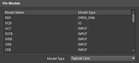
Pin Models for the chosen IBIS model.
Model Selectors
The Model Selectors region of the dialog will be populated if the chosen IBIS model has model selectors in it. This allows you to choose which model to use (e.g., a pin might have models for different voltage levels; 3.3V, 5V, etc.).
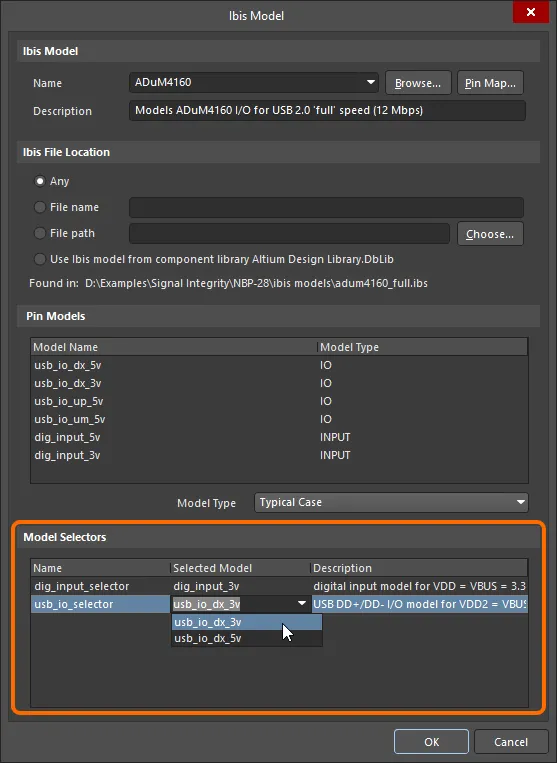
Example IBIS model with defined model selectors.
Signal Integrity Design Rules in Schematic
PCB-specific design rules for Signal Integrity can be defined in the schematic if they are added as parameters.
Supply Nets Design Rule
For Signal Integrity analysis, a PCB rule should be added to identify the supply nets and their voltage by using the Parameter Set directive. To add the supply nets design rule in the schematic:
-
Place the Parameter Set directive (Place » Directive » Parameter Set) on the appropriate net.
-
When the placed directive is selected, click the Add button in the Parameters region of the Properties panel and select Rule from the drop-down menu.
-
The Choose Design Rule Type dialog will open where the rule type can be chosen. Scroll down to the Signal Integrity rules and select Supply Nets then click OK.
-
The Edit PCB Rule (From Schematic) - Supply Nets dialog displays. Enter the voltage for this supply net and click OK. The rule entry will be listed in the Properties panel.
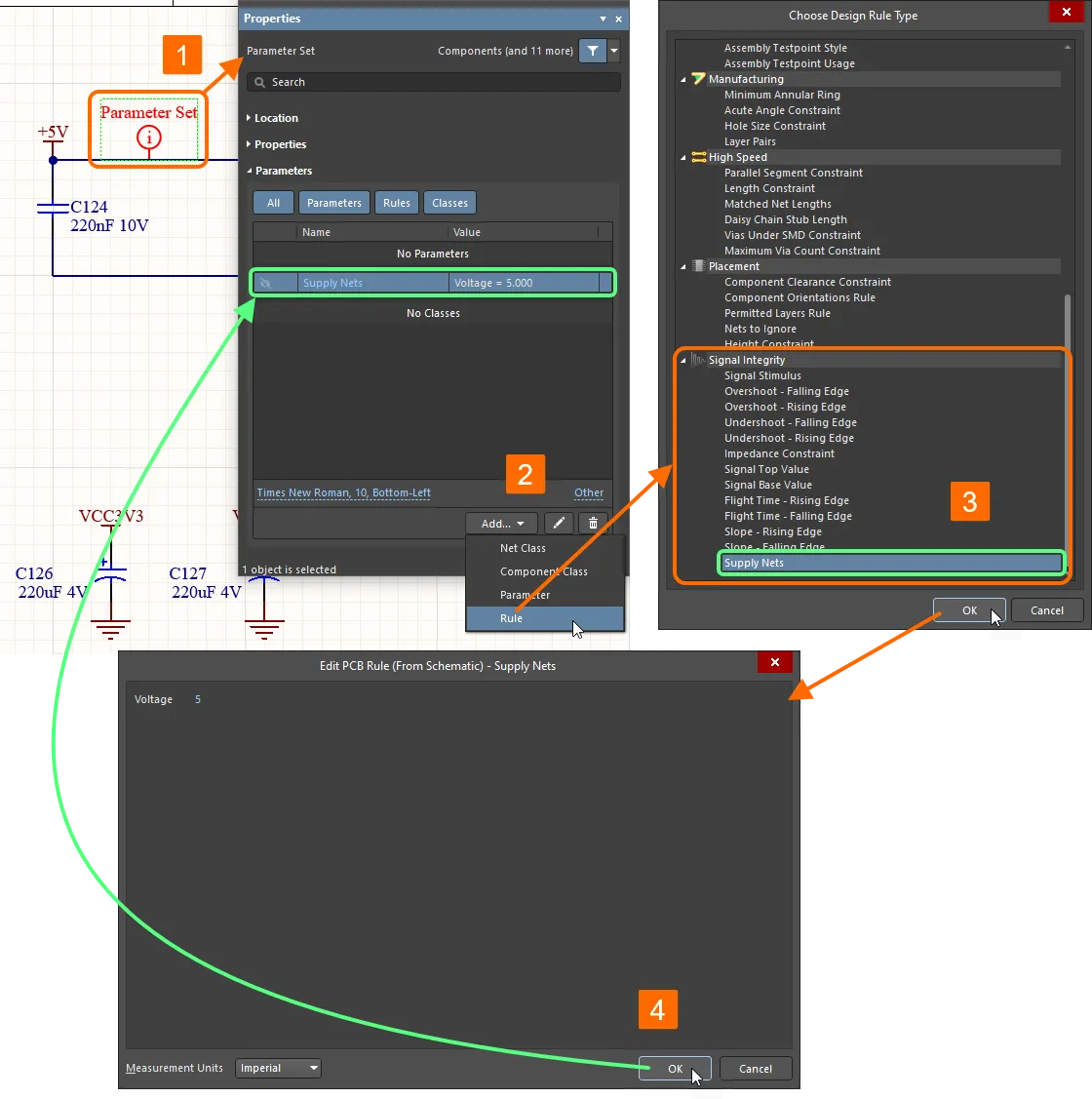
Signal Integrity design rules can be added right in schematics using the Parameter Set directives.
After transferring the design to PCB layout, the rule is added to the PCB design rules (available for viewing and editing in the PCB Editor from the PCB Rules and Constraints Editor dialog accessed using the Design » Rules command).
Note that in the schematic editor, the scope of the rule (the set of objects that the rule will target) is defined by where the parameter is added, e.g. on a wire or pin. In the PCB Editor, the scope of a rule is defined within the rule itself.
Signal Stimulus Design Rule
The other design rule that can be set up from within the schematic editor is the Signal Stimulus rule. When this rule is run, the stimulus is injected at each output pin on the net being analyzed. This requires a design rule that uses a scope of 'all', so you need to create a sheet parameter for this rule. If you do not set up this rule, the default rule options are used.
-
When no object is selected in the schematic sheet, open the Properties panel. On the Parameters tab of the panel, click the Add button and select Rule from the drop-down menu.
-
The Choose Design Rule Type dialog will open where the rule type can be chosen. Scroll down to the Signal Integrity rules and select Supply Nets then click OK.
-
The Edit PCB Rule (From Schematic) - Signal Stimulus dialog displays. Choose the stimulus kind, start level and times, then click OK. The rule entry will be listed in the Properties panel.
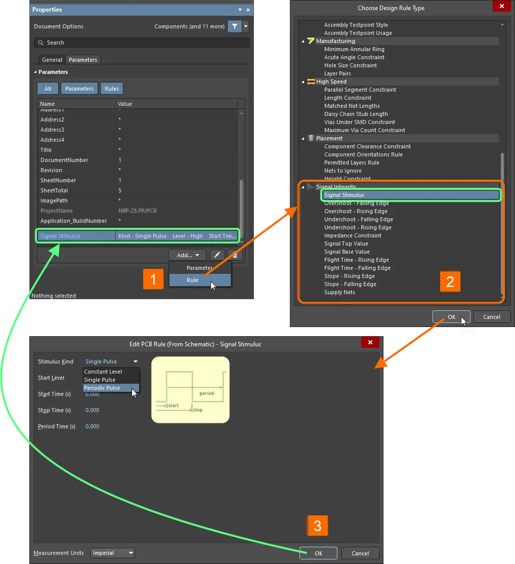
A Signal Integrity design rule can be added as a schematic sheet parameter.
Signal Integrity Design Rules in PCB
Signal Integrity parameters, such as overshoot, undershoot, impedance and signal slope requirements, can be specified as standard PCB design rules. Select Design » Rules in the PCB Editor to access the PCB Rules and Constraints Editor dialog where you can set up these rules. You can also set up these rules using parameters in the schematic editor and they will appear in the PCB Rules and Constraint Editor dialog after transferring the design to PCB layout.
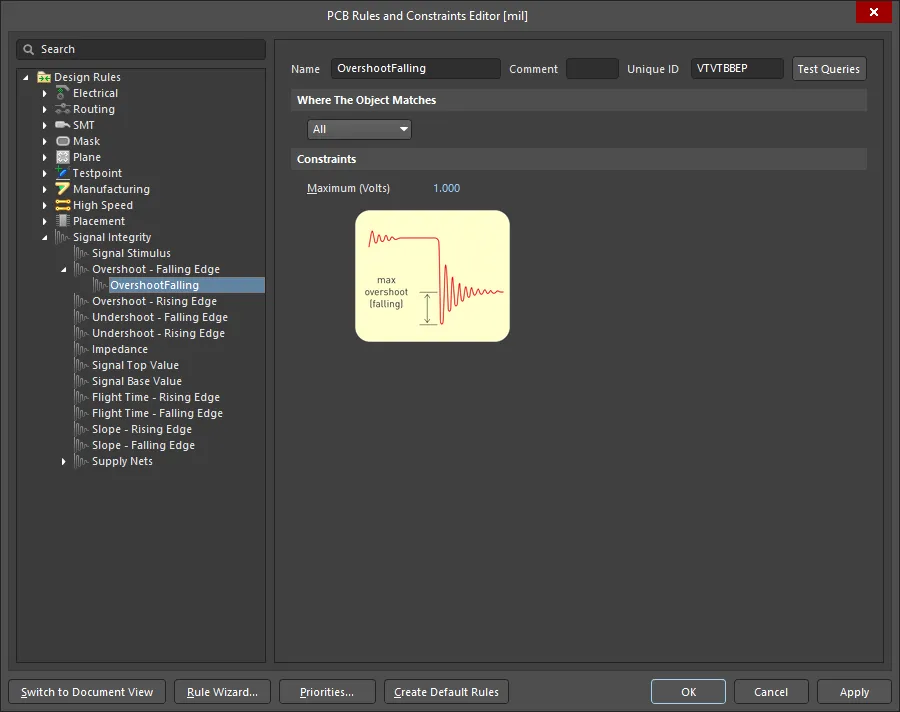
The PCB Rules and Constraint Editor dialog when browsing an Overshoot - Falling Edge design rule
These rules have two purposes. One is when running the standard DRC checks from within PCB – the board can be checked against these rules using the standard screening analysis. The second use for these rules is when using the Signal Integrity panel. These rules can be configured and enabled as tests and the panel will graphically display which nets have failed which tests.
When the design is prepared, configure and run the signal integrity analysis.
