Manufacturing Design Rule Types Available for PCB Layout in Altium Designer
The design rules of the Manufacturing category are described below.

The Manufacturing category of design rules.
Minimum Annular Ring
Default Rule: not required
This rule specifies the minimum annular ring required for a pad or via. The annular ring is measured radially, from the edge of the pad/via hole to the edge of the pad/via (also referred to as the land perimeter).
Constraints

Default constraints for the Minimum Annular Ring rule
Minimum Annular Ring (x-y) - the minimum value for the annular ring around the pads/vias targeted by the rule.
Rule Application
Online DRC and Batch DRC.
Notes
- Different fabrication houses will undoubtedly use varied and differing manufacturing technologies and equipment. Average performance houses may offer design specifications allowing a 10mil minimum annular ring. High performance houses may be able to reduce that figure down to 5mil. If pad and via holes are laser-drilled, as opposed to mechanically drilled, then the value for the minimum annular ring may be reduced further still.
- The class of board you are designing will also play a part in the value required for the minimum annular ring. For example, if your design is of IPC Class 3 standard, which refers to high reliability electronics products, the required minimum annular ring is 2mil.
- If you do have to reduce the annular ring below the accepted standard of the fabrication house, try to limit the usage of such affected pads and vias. The more pads and vias on the board that use such annular ring specifications, the more chance there is of a board failing during the fabrication process.
- To have no annular ring would, for one thing, cause poor solder joints, as there would be no copper for solder to flow onto after emerging from the pad/via barrel.
- Standards define a minimum value for the annular ring, but these values can be reduced further. The reason why they are defined at the levels they are is to guard against drill breakout. This phenomenon is fairly common when dealing with low values for the annular ring. Drill breakout occurs as a result of several manufacturing parameters (e.g. hole location, hole size, film expansion) interacting unfavorably with one another, leading to the hole being drilled in such a position as to cut through the connecting copper track(s).
- It is possible to allow controlled drill breakout, without sacrificing board performance. One method of achieving this is to apply teardrops to required pads and vias. Teardropping (otherwise known as filleting, or tapering) is the process of applying additional land area to the pad/via at the junction with any connecting track(s). This additional area protects the pad-track (or via-track) connection should a break out occur.
-
Violations of the Minimum Annular Ring design rule are detected for pads and vias with connections on layers on which pad/via shapes are smaller than the pad/via hole (e.g., if pad/via shapes have been configured manually in the Properties panel or removed by using the Remove Unused Pad Shapes tool).
Acute Angle
Default Rule: not required
This rule specifies the minimum angle permitted between any objects in the same net. The Acute Angle rule works on nets only. It finds all the acute angles created by any objects in one net. The rule essentially creates a contour from all the primitives in a net (on the same layer) and then analyzes this contour for any points that might create an angle smaller than the acute angle limit value.
Constraints

Default constraints for the Acute Angle rule
- Minimum Angle - specifies the minimum permissible angle created between objects in the same net.
- Check Tracks Only - enable this option to force the DRC to check acute angles for track objects only.
Rule Application
Online DRC and Batch DRC.
Hole Size
Default Rule: required
This rule specifies the maximum and minimum hole size for pads and vias in the design. The hole size is the diameter of the hole to be drilled through the pad/via during fabrication.
Constraints

Default constraints for the Hole Size rule
-
Measurement Method - specifies the method used in defining the minimum/maximum hole sizes:
- Absolute - the values for minimum/maximum hole sizes will be absolute values.
- Percent - the minimum/maximum hole sizes will be expressed as percentages of the pad/via size.
- Minimum - the value for the minimum hole size with respect to pads and vias in the design. The value will appear as an absolute value (Default = 1mil) or percentage of the pad/via size (Default = 20%), depending on the measurement method selected.
- Maximum - the value for the maximum hole size with respect to pads and vias in the design. The value will appear as an absolute value (default = 100mil) or percentage of the pad/via size (Default = 80%), depending on the measurement method selected.
Rule Application
Online DRC and Batch DRC.
Layer Pairs
Default Rule: required
This rule checks to ensure that the used via types match the currently defined via types. The used via types are determined from the vias and pads found in the board. The permissible via types are defined on the Via Types tab of the Layer Stack Manager.
Constraints

Default constraint for the Layer Pairs rule
Enforce layer pairs settings – specifies whether the check is made or not.
Rule Application
Online DRC, Batch DRC, and during interactive routing.
Hole To Hole Clearance
Default Rule: required
This rule ensures checking of manufacturing compatibility of drilled holes. When enabled, it will flag any multiple vias / pads at the same location, or overlapping pad / via holes. There is also an option to determine whether stacked micro vias are allowed or not.
Constraints
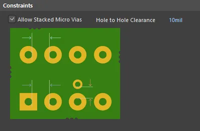
Default constraints for the Hole To Hole Clearance rule
-
Allow Stacked Micro Vias - enable this option to allow micro vias to be stacked.
- Hole To Hole Clearance - the value for the minimum permissible clearance between pad/via holes in the design.
Rule Application
Online DRC and Batch DRC.
Minimum Solder Mask Sliver
Default Rule: required
This rule helps identify narrow sections of solder mask that may cause manufacturing problems at a later stage. Ensuring that there is a minimum width of solder mask across the board, this rule checks that the distance between any two solder mask openings is equal to, or greater than, a user-specified minimum value. This includes the pads, vias, and any primitives that reside on solder mask layers. It also checks Top and Bottom sides independently.
Constraints
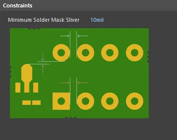
Default constraint for the Minimum Solder Mask Sliver rule
Minimum Solder Mask Sliver - specifies the minimum allowed width of solder mask.
Rule Application
Online DRC and Batch DRC.
Silk To Solder Mask Clearance
Default Rule: required
This rule checks the clearance between any silkscreen primitive and any solder mask primitive, or exposed copper-layer primitive (exposed through openings in the solder mask). The check ensures that the distance is equal to, or greater than, the value specified in the constraint.
Many manufacturers routinely strip (or 'clip') silkscreen to the mask opening and not just to the copper pad. However, doing so can render silkscreen text unreadable. Being able to catch such occurrences, through DRC, allows you to manipulate offending silkscreen text prior to sending the board to manufacturing.
Constraints
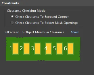
Default constraints for the Silk To Solder Mask Clearance rule
-
Clearance Checking Mode - choose a checking mode for the clearance:
- Check Clearance To Exposed Copper - in this mode, clearance checking is between silkscreen (Top/Bottom Overlay layer) objects, and copper in component pads which is exposed through openings in the solder mask.
- Check Clearance To Solder Mask Openings - in this mode, clearance checking is between silkscreen (Top/Bottom Overlay layer) objects, and solder mask openings created by objects that include a solder mask, such as pads, vias, or copper objects with the Solder Mask Expansion option enabled.
- Silkscreen To Object Minimum Clearance - specifies the minimum permissable clearance between a silkscreen object and either exposed copper, or solder mask openings, depending on the clearance checking mode chosen.
Rule Application
Online DRC and Batch DRC.
Silk To Silk Clearance
Default Rule: required
This rule defines the minimum clearance allowed between text and other objects on a silkscreen layer.
Constraints
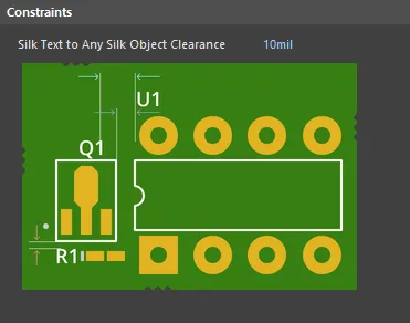
Default constraint for the Silk To Silk Clearance rule
Silk Text to Any Silk Object Clearance - specifies the minimum permissible clearance between any two silkscreen objects.
Rule Application
Online DRC and Batch DRC.
Net Antennae
Default Rule: required
This rule operates at a net level in the design to flag any open-ended track/arc primitive, or open-ended track/arc that is terminated with a via, and thus forms an antenna.
Constraints
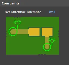
Default constraint for the Net Antennae rule
Net Antennae Tolerance - maximum permissible length for the stub of an open-ended track/arc primitive (or one that terminates in a via).
Rule Application
Online DRC and Batch DRC.
Board Outline Clearance
Default Rule: not required
This rule defines the minimum clearance allowed from design objects that are fabricated, to edges of the board. Either a single clearance value can be specified for all object-to-edge possibilities, or different clearances for different pairings can be defined, through the use of a dedicated Minimum Clearance Matrix. The terms Board Outline and Board Edge are general names used interchangeably to describe the outer edge of the board. The term edge is defined in the table below the image. The Board Outline Clearance design rule checks object-to-edge clearances on the electrical and overlay (silkscreen) layers.
Constraints
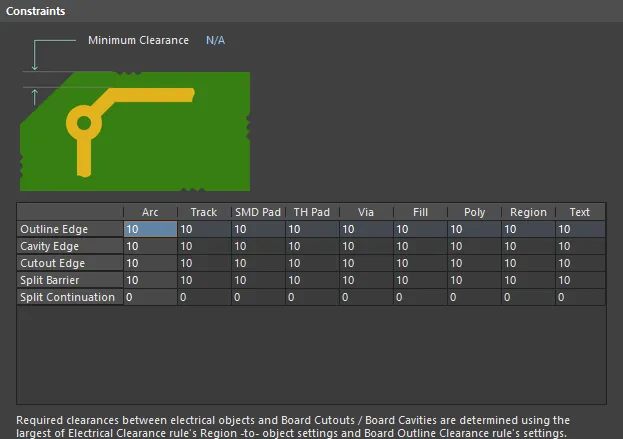
Default constraints for the Board Outline Clearance rule
| Edge Type | Definition |
|---|---|
| Outline Edge | The outer-most (exterior) edge of the board |
| Cavity Edge | The edge of a user-defined cavity |
| Cutout Edge | The edge of a user-defined cutout |
| Split Barrier | When a Split Line defines the edge of the board on this layer, this edge is referred to as a Split Line Barrier |
| Split Continuation | When this layer continues beyond a Split Line, this edge is referred to as a Split Line Continuation (a permeable boundary). To allow an object-kind to cross a Split Continuation, set the clearance value to zero. Zero indicates that for these object-kinds, this is a continuation layer, and the objects are allowed to violate (pass over) the split line. Use this technique to allow routed tracks, for example, to travel across from one Layer Stack Region to another. |
- Minimum Clearance - the value for the minimum clearance required. A value entered here will be replicated across all cells in the Minimum Clearance Matrix. Conversely, when a different clearance value is entered for one or more object pairings in the matrix, the Minimum Clearance constraint will change to N/A, to reflect that a single clearance value is not being applied across the board.
- Minimum Clearance Matrix - provides the ability to fine tune clearances between the various object-to-edge clearance combinations in the design.
Working with the Clearance Matrix
Definition of clearance values in the matrix can be performed in the following ways:
- Single cell editing - to change the minimum clearance for a specific object pairing.
-
Multi-cell editing - to change the minimum clearance for multiple object pairings:
- Use Ctrl+Click, Shift+Click, and Click+Drag to select multiple cells in a column.
- Use Shift+Click, and Click+Drag to select multiple contiguous cells in a row.
- Use Click+Drag to select multiple contiguous cells across multiple rows and columns
- Click on a row header to quickly select all cells in that row.
- Click on a column header to quickly select all cells in that column.
With the required selection made (either a single cell or multiple cells), making a change to the current value is simply a case of typing the new value required. To submit the newly entered value, either click away on another call, or press Enter. All cells in the selection will be updated with the new value.
Rule Application
Online DRC, Batch DRC, interactive routing, and autorouting.
