A logical step after creating and checking the schematic document is creating and designing the PCB. Use the File » New » PCB command to create a new PCB document. It is a good idea to configure the PCB by defining the origin, units, grid size, as well as the color display and visibility of the required layers.
Many aspects of the PCB environment setup are configured through the Properties panel in its Board mode described below. To learn more about other features for the configuration of the PCB environment, refer to the following pages:
-
Working with the Cursor-Snap System – the PCB editor includes a number of snap features, designed to help you accurately position and align design objects. Complementing the snap grid system is a hotspot snap feature, overriding the snap grid and pulling the cursor to an object's hotspot when it is within the user-definable range. This feature makes it easy to work with off-grid objects, for example routing up to the pads of an imperial component on a metric board. Together, these features are referred to as the Unified Cursor-Snap System.
-
Working with Grids & Guides – the PCB editor is a grid-based design environment - design objects are placed on what is referred to as the placement, or snap grid. There are also user-definable snap points and snap guides, as well as object axis alignment guides, all useful for the accurate positioning of objects.
-
Your View of the PCB – modern PCBs are multi-layer entities that require their clear representation in the PCB editor design space. Altium Designer features a comprehensive set of tools facilitating the display of the objects, layers, and nets that you need right now, in both 2D and 3D modes.
-
PCB Panel – the PCB panel allows you to browse the current PCB design using a range of filter modes to determine which object types or design elements are listed, highlighted, or selected.
Properties Panel
The Properties panel in its Board mode (active when no design object is currently selected in the PCB editor design space) contains options and controls for the basic configuration of the current PCB document.
The following collapsible sections contain information about the options and controls available under the panel's General tab:
Selection Filter

The options in this section of the panel determine which PCB objects may be selected in the design space.
-
All - On button – select to remove object filtering so that all types of objects may be selected.
-
Object buttons – toggle each object button to enable/disable the ability to select that object type.
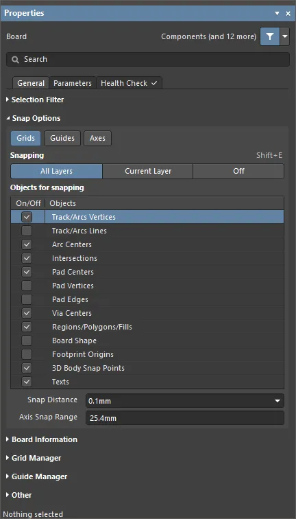
Snap Options
-
Grids – used to toggle whether the cursor will snap to the active design space grid. When this option is enabled the cursor will pull, or snap, to the nearest snap grid location. The active snap grid is displayed on the Status bar, and in the PCB editor Heads Up display.
-
Guides – used to toggle whether the cursor will snap to manually placed linear or point Snap Guides. A Snap Guide will override the Snap Grid.
-
Axes – used to toggle whether the cursor will axially align (in either the X or Y direction) to the enabled Objects for snapping. The Axis Snap Range defines the distance within which X or Y axial alignment will occur. A dynamic alignment guide line is displayed when alignment is achieved, from the current cursor location to the axially-aligned object snap point (hotspot).
-
Snapping – select directly or use the Shift+E shortcut to select whether you want to snap to objects on:
-
All Layers – enable this option to allow the cursor to snap to any electrical object on any visible layer.
-
Current Layer – enable this option to allow the cursor to only recognize and snap to objects placed on the currently selected layer.
-
Off – enable this option to turn off snapping to hotspots.
-
Objects for snapping
-
On/Off – check to enable snapping for the desired objects.
-
Objects – a list of the available objects.
-
Snap Distance – when the cursor is within this distance from an enabled object snap point (and snapping is enabled for the active layer), the cursor will snap to that point.
-
Axis Snap Range – when the cursor is axially-aligned and within this distance from an enabled object snap point (and the Axes feature is enabled), a dynamic guide line will display to indicate that alignment has been achieved.
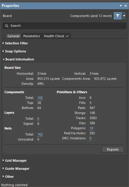
Board Information
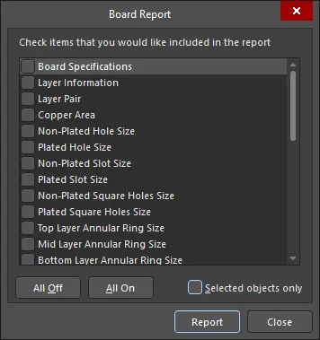
Supported items for inclusion are:
-
Board Specifications - general information about the board size and the number of components on the board.
-
Layer Information - how many primitives (arcs, pads, vias, tracks, texts, fills, regions, and component bodies) are on each used layer of the board, along with total usage for each primitive type.
-
Layer Pair - the defined drill layer pairs, along with a breakdown of the number of vias starting and stopping between those pairs.
-
Copper Area - the number of layers that contain copper areas for objects (such as board regions, board shapes, and polygon pours), the size of the copper areas (provided in inches and millimeters), and the percentage of copper areas used within each layer.
-
Non-Plated Hole Size - the number of pads and vias for each hole size of this type.
-
Plated Hole Size - the number of pads and vias for each hole size of this type.
-
Non-Plated Slot Size - the number of pads for each slot size of this type.
-
Plated Slot Size - the number of pads for each slot size of this type.
-
Non-Plated Square Holes Size - the number of pads for each hole size of this type.
-
Plated Square Holes Size - the number of pads for each hole size of this type.
-
Top Layer Annular Ring Size - the number of objects (pads and vias) for each annular ring size on the top layer.
-
Mid Layer Annular Ring Size - the number of objects (pads and vias) for each annular ring size on a mid-layer.
-
Bottom Layer Annular Ring Size - the number of objects (pads and vias) for each annular ring size on the bottom layer.
-
Pad Solder Mask - the number of pads for each specified and unique solder mask expansion value.
-
Pad Paste Mask - the number of pads for each specified and unique paste mask expansion value.
-
Pad Pwr/Gnd Expansion - the number of pads associated with unique Clearance values specified in defined power plane clearance rules.
-
Pad Relief Conductor Width - the number of pads associated with unique Conductor Width values specified in defined power plane connect style rules.
-
Pad Relief Air Gap - the number of pads associated with unique Air-Gap values specified in defined power plane connect style rules.
-
Pad Relief Entries - the number of pads associated with unique Conductors values specified in defined power plane connect style rules.
-
Via Solder Mask - the number of vias for each specified and unique solder mask expansion value.
-
Via Pwr/Gnd Expansion - the number of pads associated with unique Clearance values specified in defined power plane clearance rules.
-
Track Width - the number of objects for each unique track width used in the design.
-
Arc Line Width - the number of objects for each unique arc line width used in the design.
-
Arc Radius - the number of objects for each unique arc radius used in the design.
-
Arc Degrees - the number of objects for each unique arc angle used in the design.
-
Text Height - the number of objects for each unique text height used in the design.
-
Text Width - the number of objects for each unique text width used in the design.
-
Polygon Clearance - the number of polygons of each clearance used in the design.
-
Net Track Width - the number of net tracks of each width used in the design.
-
Net Via Size - the number of net vias of each size used in the design.
-
Routing Information - information on routing completion (as a percentage), along with a breakdown of the total number of connections, how many have been routed, and how many remain.
Enable the Selected objects only option to have the report generate information for each of the include items, but only with respect to design objects currently selected in the main design space. Note that to use this option, you will need to select the required objects in the design space, then access the dialog through the PCB Editor's Reports menu - since accessing the Board mode of the Properties panel is only possible when no objects are selected.
-
Once all required items are enabled for inclusion in the report, click the Report button to generate the report.
-
The report is generated in Text and/or HTML formats, according to the settings in the PCB Editor – Reports page of the Preferences dialog.
-
The report files are named <PCBDocumentName>.txt and/or <PCBDocumentName>.htm, and are created in the same folder as the PCB file. The HTML version has the HTML Title, Board Information Report.
Grid Manager

-
Grid Manager – where local customized grids can be defined and managed, as well as the default Snap Grid for the board.
-
Priority – in the design space, priority is distinguished by drawing order. The highest priority grid (priority
1) will be drawn in front of all other grids, then the grid with priority level 2, etc., down to the default Global Board Snap Grid, which is drawn behind all other custom grids.
-
Name – displays the name of the grid.
-
Color – click to open a drop-down to set/change the color of the associated grid.
-
Origin – enable to display an origin marker in the design space.
-
Comp – enable to apply the selected grid to only components.
-
Non Comp – enable to apply the selected grid to objects that are not components.
-
Add
-
Add Cartesian Grid – click to add a Cartesian grid.
-
Add Polar Grid – click to add a Polar grid. Polar grids enable you to more easily design non-rectangular features and boards.
-
Properties – click to open the respective grid editor dialog (Cartesian Grid Editor or Polar Grid Editor) to modify properties for the selected grid.
-
 – click to delete the currently selected grid.
Guide Manager

-
Guide Manager – where a range of manual Snap Guides and Snap Points for the board can be defined and managed.
-
Add – click to add a new snap guide or snap point. Choose the corresponding command for the required guide type from the associated menu; an entry for the new guide/point will be added to the grid. The following guide types are available:
-
Add Horizontal Guide – use this command to add a horizontal guideline at the desired Y-coordinate location in the design space.
-
Add Vertical Guide – use this command to add a vertical guideline at the desired X-coordinate location in the design space.
-
Add +45 Guide – use this command to add a 45 degree (y=x) guideline that passes through the desired X,Y coordinate location in the design space.
-
Add -45 Guide – use this command to add a -45 degree (y=-x) guideline that passes through the desired X,Y coordinate location in the design space.
-
Add Snap Point – use this command to add a point snap guide. This is a hotspot that you manually mark within the confines of the default snap grid. During an interactive process such as placing or moving an object, that objects' hotspot will 'snap' to a point snap guide when it passes into close proximity with it.
-
Place – click to place a guide. Select the guide type from the drop-down:
-
Place Horizontal Guide – use this command to place a horizontal guideline at the desired Y-coordinate location in the design space.
-
Place Vertical Guide – use this command to place a vertical guideline at the desired X-coordinate location in the design space.
-
Place +45 Guide – use this command to place a 45 degree (y=x) guideline that passes through the desired X,Y coordinate location in the design space.
-
Place -45 Guide – use this command to place a -45 degree (y=-x) guideline that passes through the desired X,Y coordinate location in the design space.
-
Place Snap Point – use this command to place a point snap guide. This is a hotspot that you manually mark within the confines of the default snap grid. During an interactive process such as placing or moving an object, that objects' hotspot will 'snap' to a point snap guide when it passes into close proximity with it.
-
 – click to delete the currently selected guide.
Guides are only visible when the Show Grid option is enabled in the View Options tab of the View Configurations panel (show image![]() ).
).
Other
-
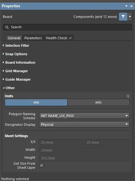
Units – use to select the default measurement units for the current PCB document. Default units are used to display any distance-related information on screen or in reports. The default units are always used if a unit's suffix (mm or mil) is not entered when specifying any distance-related information.
-
Select View » Toggle Units (or press the Q shortcut) to switch the design space units between imperial and metric.
-
When a dialog or panel is active, press Ctrl+Q to toggle the units of all measurements in that dialog or panel.
-
Regardless of the current setting for the units, you can include the units when entering a value in a dialog or panel to force that value to be used.
-
Polygon Naming Scheme – select a naming system from the drop-down menu. There are four choices of naming templates:
-
NET NAME_LXX_PXXX
-
LXX_NET NAME_PXXX
-
NET NAME_LAYER NAME_PXXX
-
LAYER NAME_NET NAME_PXXX
where:
-
NET NAME – name of the net to which the polygon is connected. If the polygon is not connected to a net, the name NONET is used.
-
LAYER NAME – user-defined name of that layer from the Layer Stack.
-
LXX – system assigned copper layer number based on the current order of layers in the Layer Stack where Top Layer is L01. This value is updated whenever the order of copper layers is changed.
-
PXXX – system-assigned numerical index; unique for each polygon on the board.
Design changes, such as moving a layer in the layer stack, renaming a net, or changing the naming scheme will result in automatic name changing. Affected design rules are automatically updated.
-
Designator Display – use this field to determine how designators are to be displayed. It can be difficult positioning the designator strings in a multi-channel design, as they can end up being quite long. As well as choosing a naming option that results in a short name, another option is to display just the original, logical component designation instead. For example, C30_CIN1 would display as C30. This would of course necessitate some other notation being added to the board to indicate the separate channels, such as a box being drawn around each channel on the component overlay. The following options are available:
-
Physical – choose to display the physical designators. These are the designators displayed on the compiled tab views of the schematic source documents. For multi-channel designs, designator format is determined by the Designator Format field on the Multi-Channel tab of the Project Options dialog. Physical designators are unique, e.g., R1_CH1.
-
Logical – choose to display the logical designators. These are the designators displayed on the Editor tab views of the schematic source documents. Logical designators are not unique; for example, the R1_CH1 physical designator will become simply R1.
-
Sheet Settings – use this region to configure the PCB sheet.
-
X/Y – enter the X and Y coordinates for the bottom left corner of the sheet. This distance is measured from the absolute origin, which is the bottom left corner of the design space. The distance can be defined in either metric or imperial units regardless of the default units (which are determined by the Units setting). To specify the units when entering a size, add the mm or mil suffix to the value.
-
Width – enter a width for the sheet here. The sheet provides an area that emulates the traditional drawing sheet and is useful for placing information such as dimensions, notes and title blocks. Information placed on mechanical layers can be linked to the sheet so that they only display when the sheet is being displayed. Sheet size can be defined in either metric or imperial units regardless of the default units (which are determined by the Units setting). To specify the units when entering a size, add the mm or mil suffix to the value.
-
Height – enter a height for the sheet here. The sheet provides an area that emulates the traditional drawing sheet and is useful for placing information such as dimensions, notes and title blocks. Information placed on mechanical layers can be linked to the sheet so that they only display when the sheet is being displayed. Sheet size can be defined in either metric or imperial units regardless of the default units (which are determined by the Units setting). To specify the units when entering a size, add the mm or mil suffix to the value.
-
Get Size From Sheet Layer – enable this option to size the sheet from the sheet layer.
The following collapsible section contains information about the options and controls available under the panel's Parameter tab:
Strings
-
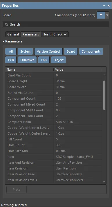
Buttons – toggle each button to show/hide related parameters in the grid table below.
-
Grid – lists the Name and Value of the parameters associated with the current PCB document. The grid lists both system parameters (e.g., the PCB file name) and the parameters calculated from the PCB (e.g., the number of components on the PCB and the board thickness).
-
Place – click to place the currently selected parameter as a special string. The special string will be placed on the layer defined as the default layer for Text objects on the PCB Editor - Defaults page of the Preferences dialog.
Health Check
The panel's Health Check tab provides an interface to the PCB Health Check Monitor. To learn more about this functionality, see PCB Health Check Monitor.
When an Object is Selected
When a design object is selected, the panel will present options specific to that object type. The following table lists the object types available for placement within a PCB document – click a link to access the properties page for that object.
Although
Tracks and
Lines are actually the same object, the difference is how the software behaves during their placement, which is why there are different commands.
After launching the Place » Line command, the cursor will change to a cross-hair and the editor will enter line placement mode. Placement is made by performing the following actions:
-
Click to define the starting position of the line.
-
Move the cursor to set the length and angle the line then click again to complete placement.
-
Continue placing further lines, or right-click or press Esc to exit the placement mode.
