
KB: 구성 요소를 서로 가까이 배치할 수 없음
Created: March 25, 2021 | Updated: November 15, 2024
Starting in version: 18
Up to Current
이 기사에서는 PCB 상의 다른 구성 요소와 가까이 배치할 수 없는 전형적인 시나리오에 대해 설명합니다.
Solution Details Copy Link Copied
While moving / placing a component, there are three component placement modes . The current mode can be set through: Preferences ► PCB Editor ► Interactive Routing ► Dragging ► Component Pushing.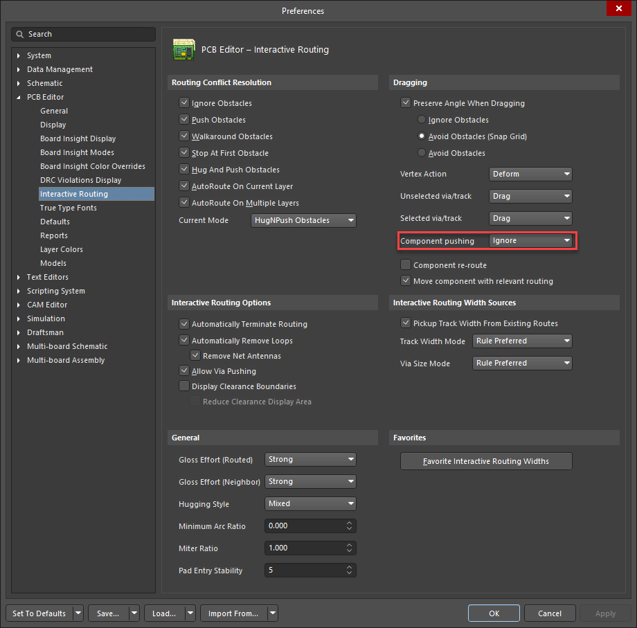
You can also switch between the modes while directly on the PCB by pressing the key "R" while dragging the component as described here:
Press the R key to cycle through component push modes. The following modes are supported:
- Ignore - default behavior, where the component can be moved regardless of creating a violation with neighboring component(s). In this mode, the same component clearance checking routines seen in previous versions of Altium Designer are used. These routines use the 3D body (if there is one) or the copper and silk primitives to identify an object's clearance.
- Push - the component will push other components away to provide compliance with clearances between components. Components in unions can be pushed and the location of components in the union may change, but the union will not break. Locked components can not be pushed. In this mode, components are identified by their selection boundary, which is the smallest possible rectangle that encloses all of the primitives in the component.
- Avoid - the component will be forced to avoid violating clearance rules between other components. In this mode, components are identified by their selection boundary, which is the smallest possible rectangle that encloses all of the primitives in the component. (https://www.altium.com/documentation/altium-designer/pcb-cmd-moveobjectmoveobject-ad)

In either Push or Avoid mode, how closely you can place two components together is dictated by Component Clearance rule as well as configurable component selection bound box (i.e. rectangle) which may include, say, pin 1 indicator on silkscreen.
It is highly advisable to make use of Courtyard layer to define the component boundary explicitly at the time of footprint creation.
you may want to consider adding Courtyard layer for each of your component (if there is no 3D Body layer).
Here are the numbers of resources on Courtyard layer and how it can be leveraged:
https://www.altium.com/documentation/altium-designer/working-with-mechanical-layers#!component-layer-pairs:~:text=on%20the%20board.-,Courtyard,-%E2%80%93%20used%20to%20define
https://www.altium.com/documentation/altium-designer/altium-designer-19-1-new-features-and-updates-summary-ad?version=19.1#!enhancedcomponent-selection
https://www.altium.com/documentation/altium-designer/nfs-20-0pcb-component-shape-detection-improvements-ad?version=20.0
https://www.youtube.com/watch?v=d2vEi3tdO9g
https://resources.altium.com/p/how-to-setup-and-use-courtyard-assembly-and-other-component-layer-pairs-how-to-adscvid