There is a saying that PCB design is 90% placement and 10% routing. While you could argue about the percentage of each, it is generally accepted that good component placement is critical for good board design. Remember that you may also need to tune the placement as you route.
The component footprint defines the space and connection points needed to mount the physical component on the printed circuit board. It is a group object made up of a collection of simple primitive objects, including pads, lines and arcs, as well as other design objects.
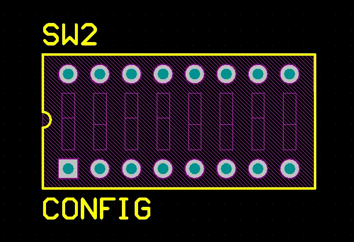
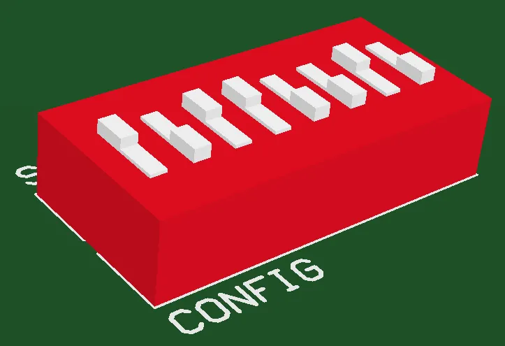
The component footprint defines the component mounting and connections on the PCB and can also include 3D body objects to define the actual component.
The pads provide the mounting and connection points for the component pins. Additional design primitives, such as lines and arcs, are often included to define the outline of the component shape on the component overlay (silkscreen) layer.
The component footprint can also include optional 3D body objects, which define the physical space or envelope of the actual component that is mounted on the board. If the physical component has been defined using 3D body objects or imported STEP models, three-dimensional component clearance checking can be performed.
Component footprints are created in the PCB footprint editor by placing suitable design objects to create the shape required to mount and connect the component. The component reference point is the origin of the PCB footprint editor design space, which can be set in the editor to: pin 1, the geometric center, or a user-defined location on the component. To learn more about footprint creation, refer to the Creating a PCB Footprint page.
Component Properties
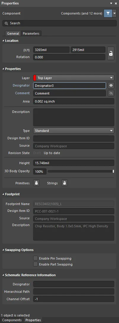
The Component mode of the Properties panel.
General Tab
Location
The

icon to the right of this region must be displayed as

(unlocked) in order to access the below fields. Toggle the lock/unlock icon to change its lock status.
Properties
-
Layer – sets the layer on which the component is placed. Components can be assigned to the Top layer or Bottom layer. Use the drop-down to select a different layer. Changing the layer status swaps all of the component primitives to each layer's respective opposite layer. For example, moving a Top layer component to the bottom layer means single layer pages are swapped from the top to the bottom layer, primitives on the Top Overlay are reassigned to the Bottom Overlay, and primitives on a paired mechanical layer are swapped to the other mechanical layer in that pair. The orientation of the component will be flipped along the X-axis and the component overlay text will read from the bottom.
-
Reuse Block – when the component is a part of a reuse block, this field shows the name of the parent reuse block. Click the Reuse Block hyperlink to see the properties of this reuse block.
-
Designator – the designator of the component is an alphanumeric string of up to 255 characters. Each component must have a unique Designator string. Toggle  or
or  to show/hide the designator. Click the Designator hyperlink to open the properties of the component's designator.
-
Comment – the comment of the component is an alphanumeric string of up to 255 characters. Toggle  or
or  to show/hide the comment. Click the Comment hyperlink to open the properties of the component's comment.
-
Area – the area of the placed component displayed in the current board units. The area can be user-defined, if it is not it is automatically calculated from the component's selection area:
-
To define the component area, edit the Area in the Properties panel for the footprint in the PCB Footprint editor. To push an updated footprint to an open PCB, right-click on the footprint name in the PCB Library panel, then select Update PCB With <ComponentName> from the context menu.
-
You can also user-define the area of a component already placed on a PCB by selecting the component and then entering the value in this field.
-
To switch from a user-defined area to a calculated area for a component placed on a PCB, delete the value in this field; the field will automatically be re-populated with the auto-calculated value.
-
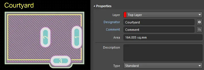
The automatically calculated area is the area that is highlighted when you click to select the component. The selection area is determined from the geometries on the Courtyard layer, i.e. when that layer is not present, the combination of the geometries on the Silkscreen, 3D Body objects, and Copper layers (strings are excluded). The upper images displayed below show the component's area when there is an outline defined on the courtyard layer; the lower image shows the area when it is calculated from the geometries on the Silkscreen, 3D Body objects, and Copper layers.
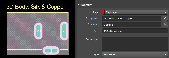
-
The edge of the Courtyard is the centerline of the outline tracks and arcs that form the Courtyard boundary.
-
Arcs can be used to create a curved component Courtyard shape, as shown in the upper image above, where the Courtyard curves around pad 3.
-
The Area field displays the area of the selected component. If multiple components are selected, it will display the area of one component if all selected components have the same area, or it will display * if they have different area values. To calculate the area of multiple selected components, use the List panel to display the areas of those components. From there, you can right-click and copy the values, then paste them into a spreadsheet and calculate their sum (show image).
► Learn more about how the selection area is calculated and the other modes available to determine the selection area.
► Learn more about Working with Mechanical Layers.
-
Description – component-level description of this component. Typically, the description is defined during component creation, but it can also be edited/added to the component on the schematic. This is the description shown in the Components panel.
-
Type – select one of the following component types for the component footprint here. The available types are:
-
Standard – these components possess standard electrical properties, are always synchronized between the schematic and PCB (the footprint, pins/pads and net assignments must all match), and are included in the BOM. An example is a standard electrical component, such as a resistor.
-
Mechanical – these components do not have electrical properties, are not synchronized (you must manually place them in both editors), and are included in the BOM. An example is a heatsink.
-
Graphical – these components do not have electrical properties, are not synchronized (you must manually place them in both editors), and are not included in the BOM. An example is a company logo.
-
Net Tie (in BOM) – these components are used to short two or more different nets together. They are always synchronized between the schematic and PCB (the footprint, pins/pads and net assignments must all match), and are included in the BOM. They differ from a Standard component in that connectivity created by copper within the footprint is not checked – it is this copper that allows the nets to be shorted. Note: enable the Verify Shorting Copper option in the Design Rule Checker dialog to verify that there is no unconnected copper within the component.
-
Net Tie – these components are used to short two or more different nets together. They are always synchronized between the schematic and PCB (the footprint, pins/pads and net assignments must all match), and are not included in the BOM. They differ from a Standard component in that connectivity created by copper within the footprint is not checked – it is this copper that allows the nets to be shorted. Note: enable the Verify Shorting Copper option in the Design Rule Checker dialog to verify that there is no unconnected copper in the component.
-
Standard (No BOM) – these components possess standard electrical properties, are always synchronized between the schematic and PCB (the footprint, pins/pads and net assignments must all match), and are not included in the BOM. An example is a testpoint component that you wish to exclude from the BOM.
-
Jumper – these components are used to include wire links in a PCB design, for example, on a single-sided PCB that cannot be fully routed on one layer. For this component type, the component footprint and pins are synchronized between the schematic and PCB but the net assignments are not, and the component is included in the BOM. As well as selecting this option at the component level, both of the pads in the component must have their JumperID set to the same non-zero value. Jumper-type components do not need to be wired on the schematic; they only need to be included on the schematic if they are required in the BOM. If they are not required in the BOM, they can be placed directly in the PCB where the Component Type is set, the JumperIDs are set, and the Nets manually assigned for the pads.
-
Design Item ID – displays the Design Item ID for the selected component. This field is not editable.
-
Source – displays the source document of the component. Click  to open a dialog to browse and select a different source document.
-
Revision State – shows the state of the revision of the Workspace library component in terms of its lifecycle state and also its revision status, i.e. whether it is the latest released revision of that component (Up to date) or is an earlier revision (Out of date).
-
Height – a height field for the component. This field defined the height of the PCB component before the introduction of the 3D Body object, however the 3D model provides a superior method of defining the component height for tasks such as 3D collision detection. Note that the value defined in this Height field is used by Altium MCAD CoDesigner, not the height of the 3D model (learn more).
-
3D Body Opacity – enter the desired opacity percentage or use the slider bar.
-
Primitives – click the associated lock icon to lock/unlock.  – lock all the primitives of the component so that it can be treated as a single object.
  – unlock to modify the individual primitives that make up the component. After editing, the component primitives should be re-locked.
-
Note that when component primitives are locked, most of their properties cannot be modified by graphical (e.g., using drag-and-drop) or non-graphical (e.g., using the Properties or a List panel) editing methods.
-
Note that component pad properties can be accessed and modified if required without unlocking the primitives by double-clicking directly on the pad.
-
Strings – click the associated lock icon to lock/unlock.  – lock all the strings of the component.
  – unlock to modify the strings of the component.
Select the clickable links of the Designator and Comment from the Component mode of the Properties panel to be redirected to those objects' respective Properties panels, where you can edit their options.
Footprint
-
Footprint Name – displays the name of the footprint corresponding to the chosen component.
-
Design Item ID – the identification of the chosen component.
-
Source – name of the Workspace in which the chosen component has been placed.
-
Description – description of the component footprint, defined in the PCB footprint editor.
Swapping Options
-
Enable Pin Swapping – check to allow the pin swapping function.
-
Enable Part Swapping – check to allow the part swapping function (e.g., four parts of a 74 series IC).
Schematic Reference Information
When the design is initially transferred, schematic reference information is transferred from the schematic to the PCB editor. To refresh this data at a later stage, click the Perform Update button in the Edit Component Links dialog.
-
Designator – the designator of the schematic component to which this PCB component has been matched.
-
Hierarchical Path – displays where, in the hierarchical structure of the schematic, this component can be found.
-
Channel Offset – when a design is first transferred from schematic to PCB, each component on each schematic sheet is given a unique channel offset.
Parameters Tab
-
Table – displays the Name, Value, and Source of each listed parameter.
Component Designators and Comments
The designator and comment fields are a child parameter object of a PCB component (part). The designator is used to uniquely identify each placed part to distinguish it from all other parts placed in all the PCB documents in the project. The comment is used to add additional information to a placed object. Both comment and designator are configured after the parent component part object is placed. It is not a design object that you can directly place.
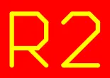
A placed Designator object

A placed Comment object
PCB 2D/3D component designators will auto-increment by one during placement if the initial component has a designator ending with a numeric character. Change the designator of the first component prior to placement from the Properties panel.
To achieve alpha or numeric designator increments other than 1, use the Paste Array feature. Controls for this feature are provided in the Setup Paste Array dialog, accessed by pressing the Paste Array button in the Paste Special dialog (Edit » Paste Special).
The graphical method of editing allows you to select a placed designator or comment object directly in the design space and change its location, rotation, orientation, and size.
When a designator or comment object is selected, the following editing handles are available:
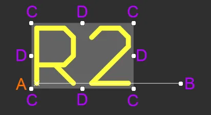
A selected Designator
-
Click and drag B to rotate the designator/comment about its reference point A (denoted by the small x).
-
Click and drag C to resize the designator's/comment's bounding box in the vertical and horizontal directions simultaneously.
-
Click and drag D to resize the designator's/comment's bounding box in the vertical and horizontal directions separately.
-
Click anywhere on the designator/comment away from editing handles and drag to reposition it. While dragging, the comment can be rotated or mirrored:
-
Press the Spacebar to rotate the designator/comment counterclockwise or Shift+Spacebar for clockwise rotation. Rotation is in accordance with the value for the Rotation Step defined on the PCB Editor – General page of the Preferences dialog.
-
Press the X or Y keys to mirror the designator/comment along the X-axis or Y-axis.
The properties of a Designator or Comment object can be modified in the Parameter mode of the Properties panel.
The
Tools » Add Designators for Assembly Drawing command from the main menus can be used to automatically add and update assembly component designators on the
Designator Component Layer Pair within the PCB document. After launching the command, a dialog will appear displaying the total number of assembly component designators that were added/updated. If the PCB document does not include the
Designator Component Layer Pair, a dialog will open suggesting adding the Component Layer Pair.
Parameter Properties
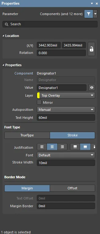
The Parameter mode of the Properties panel.
Location
-
(X/Y)
-
X (first field) - the current X (horizontal) coordinate of the reference point of the designator relative to the current workspace origin. Edit to change the X position of the designator. The value can be entered in either metric or imperial; include the units when entering a value whose units are not the current default.
-
Y (second field) - The current Y (vertical) coordinate of the reference point of the designator relative to the current origin. Edit to change the Y position of the designator. The value can be entered in either metric or imperial; include the units when entering a value whose units are not the current default.
-
Rotation - the designator's angle of rotation (in degrees) measured counterclockwise from zero (the 3 o'clock horizontal). Edit to change the rotation of the designator. Minimum angular resolution is 0.001°.
Properties
-
Parameter type - displays the type of parameter (Component, Sheet Symbol, etc.) and parameter name.
-
Name - the name of the designator.
-
Value - use this field to enter the desired value of the designator. Click the eye icon to toggle the value between being visible and not visible in the design space.
The display of the designator or comment can be toggled between not hidden and hidden for a placed component by right-clicking the component in the design space and choosing the
Component Actions » Hide Designator /
Component Actions » Show Designator or
Component Actions » Hide Comment /
Component Actions » Show Comment command, respectively, from the context menu.
-
Layer - use the drop-down to select the desired layer. Enable Mirror if desired.
-
Autoposition - use the drop-down to select the desired automatic position in relation to the associated object.
-
Text Height - use this field to enter the desired text height.
-
Font Type
-
Border Mode
-
Margin - click this button to enable the editing of the Margin Border option.
-
Text Offset - the amount the designator is offset back from the edge/corner that it is justified against. This option has no effect when the Center justification mode is chosen. This option is not available for Margin.
-
Offset - click this button to enable the editing of the Text Offset option.
-
Margin Border - use to specify the size of the margin border surrounding the designator. This option is not available for Offset.
Component Availability on the PCB
When the design is transferred from the schematic editor to the PCB editor, PCB component footprints are automatically placed from the available libraries. This is called Design Synchronization, which is a process to detect and resolve the differences between the schematic and the PCB.
Altium Designer supports a set of tools facilitating the placement of the required component footprint in the PCB design space. See the following pages to learn about these tools:
Browsing Placed Components
In the PCB panel’s Components mode, its three main regions change to reflect the component hierarchy of the current PCB design (in order from the top):
-
Component Classes
-
Components within a class
-
Component Primitives
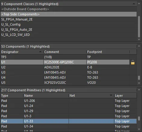
The PCB panel regions allow a cumulative filter selection through component classes to individual components to component primitives.
Right-click on a component or component primitive entry then choose the Properties command (or double-click on the entry directly) to access the Properties panel, in which you can view/modify the properties of the component/primitive as required.
Right-click on a component class entry, then choose Properties (or double-click on the entry directly) to open the Edit Component Class dialog for that class. From the dialog, you can view/modify the component membership of the class, rename it, or add additional classes.
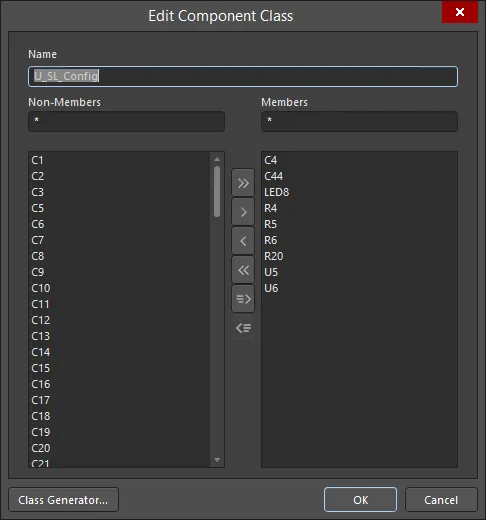
Editing a selected component class.
The display/inclusion of each component primitive type in the Component Primitives region of the panel depends on whether the corresponding option for each has been enabled on the right-click menu accessed from either the Components or Component Primitives regions.

Right-click on a component or component primitive entry to select the items to include.
While browsing, components can be easily locked or unlocked by double-clicking in the box to the right of the Footprint column in the Components region.
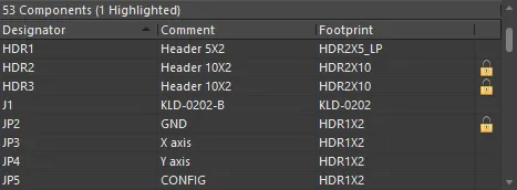
Locking/Unlocking from the PCB panel saves you from having to navigate through the Properties panel.
Component Selection Bounding Box
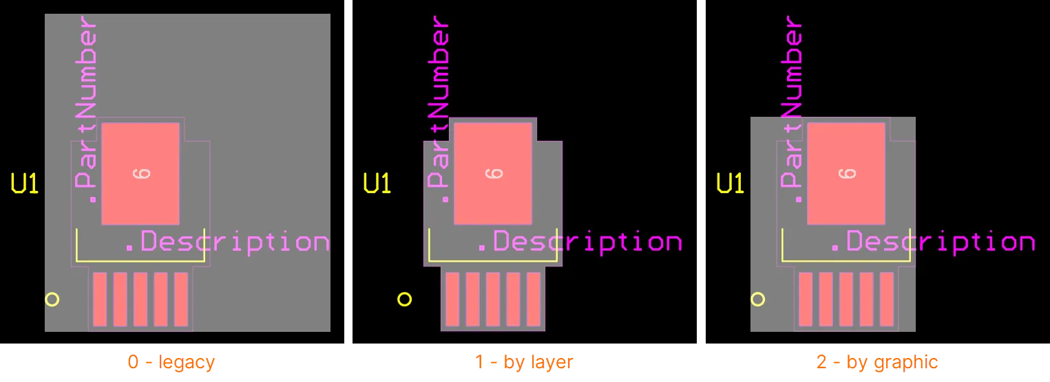
When you click and select a component, the selection bounding box appears. To control which layers are used to define the bounding box, the PCB.ComponentSelection option in the Advanced Settings dialog can be used. The option supports three modes (enter the value 0, 1 or 2; the default mode is 2):
-
0 - legacy mode - this mode combines geometries from all layers except the Silkscreen Designator and Comment strings.
-
1 - by layer mode - use the geometries from the first of the layers listed below that contains objects, with the following priority:
-
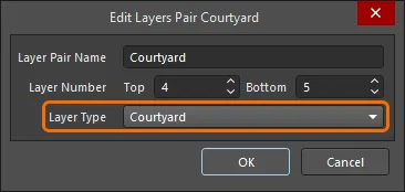
Courtyard Layer Type
-
3D Body Layer (STEP models are stored in a 3D Body object sized to the smallest rectangular prism that holds the model. For component selection, this 3D Body is used, not the shape of the STEP model)
-
Silkscreen Layer plus Copper Layers
-
Copper Layers
-
2 - by graphic mode - this mode combines the geometries detected on the Courtyard Layer Type, the Silkscreen, 3D Body objects, and Copper layers. Strings are excluded.
-
References to the Courtyard layer are for a Component Layer Pair with the Layer Type = Courtyard, the name of the layer pair is not considered.
-
If the component includes a 3D model, the actual 3D model shape is used for component collision checking, while the shape of the component selection box is determined as described above.
-
Mechanical layer objects are excluded from the selection bounding box but are included in the collision checking bounding box when there are no 3D Bodies or Courtyard layer objects defined. The exceptions to this are the .Designator and .Comment text strings, which are always excluded. Learn more about Working with Mechanical Layers.
-
When the selection bounding box of a component is defined by the courtyard layer tracks, the centerline of these tracks is used to define the bounding box (as selecting the component shows – 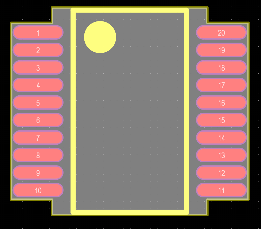 ). Note that this is only the case when the shape defined on the courtyard layer is a closed shape, with the track end vertices being coincident (exactly touching). Otherwise, the bounding box is defined by the smallest rectangle that encloses all of the objects on the courtyard layer.
-
The component selection bounding box is used to calculate the component area and during component placement in Push and Avoid Obstacles placement modes.
Adding Primitives to a Component
Selected primitives can be added to a component by choosing the Tools » Convert » Add Selected Primitives to Component command from the main menus. After selecting a command, choose the component to which you want to add the selected primitives. When confirmed, the new primitives will be recognized as part of the single component object and may be used in conjunction with the component's original primitives.
The target component must have its primitives unlocked to carry out this operation. Use the Primitives lock icon in the component's properties to unlock component primitives.
Exploding a Component to Primitives
A component can be converted to its constituent primitive objects using the Tools » Convert » Explode Component to Free Primitives command from the main menus or by right-clicking over a placed component (selected or not) and then choosing the Component Actions » Explode Component To Free Primitives (or Explode Selected Components To Free Primitives) command from the context menu. An exploded component is no longer a component, so the designator and comment will be removed, and the component will revert to the various primitives from which it was made.
Explode has no effect on the footprint model stored in the applicable source library, only on the converted instance(s) of the component(s) placed on the PCB document.
-
Explode is a one-way process; there is no command to regroup an exploded component. However, you can use the Undo command to achieve this.
-
The Explode command should not be used to modify a component's properties. A component's primitives can be edited by unlocking them (using the Primitives lock icon in the component's properties), editing them as required, and then re-locking them.
Accessing Clickable Links to Reference Information
When named document links have been added to the component, the indicated document/page URL - specified through a defined underlying URL link parameter - for the selected component or the component under the cursor can be opened. This feature allows named document links that have been transferred from schematic components to be presented as named PCB component links to PDFs, text files, or HTML pages. That occurs when the named document links for the component have been updated from the Schematic to the PCB (Design » Update PCB Document). During that update process (via an ECO), the schematic-named document links are converted to ComponentLink parameter pairs (ComponentLinknDescription/ComponentLinknURL) for the matching PCB component. For example:
| Schematic Component Parameter |
|
PCB Component Parameters |
| Name |
Url |
⇒
|
Name |
Value |
STM32 Family Web Page |
http://www.st.com/stm32 |
ComponentLink1Description |
STM32 Family Web Page |
ComponentLink1URL |
http://www.st.com/stm32 |
The link index number (n) used in the component parameters will define the ordered position of the matching PCB Component Link in the References submenu. With a component on the PCB selected, the defined ComponentLink parameter pairs are presented in the Parameters section of the Properties panel.
After launching the command, the web-based URL target page or indicated document will open directly (if available).
-
A web-based URL will be open either in an external browser, or as a tabbed document within Altium Designer, as determined by the Open internet links in external Web browser option, on the System - View page of the Preferences dialog. Keep in mind that to open in an external browser, the value (URL) of the link parameter must include the http:// prefix.
-
For more information about establishing document link parameters in the schematic space, refer to the Schematic Libraries page.