This rule specifies the maximum and minimum hole size for pads and vias in the design. The hole size is the diameter of the hole to be drilled through the pad/via during fabrication.
This rule checks to ensure that the used via types match the currently defined via types. The used via types are determined from the vias and pads found in the board. The permissible via types are defined on the Via Types tab of the Layer Stack Manager.
Default Rule: required i
This rule ensures checking of manufacturing compatibility of drilled holes. When enabled, it will flag any multiple vias / pads at the same location, or overlapping pad / via holes. There is also an option to determine whether stacked micro vias are allowed or not.
Constraints
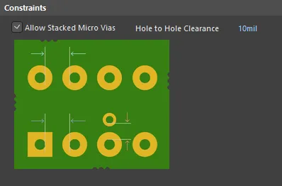
Default constraints for the Hole To Hole Clearance rule
Rule Application
Online DRC and Batch DRC.
Minimum Solder Mask Sliver
Default Rule: required i
This rule helps identify narrow sections of solder mask that may cause manufacturing problems at a later stage. Ensuring that there is a minimum width of solder mask across the board, this rule checks that the distance between any two solder mask openings is equal to, or greater than, a user-specified minimum value. This includes the pads, vias, and any primitives that reside on solder mask layers. It also checks Top and Bottom sides independently.
Constraints
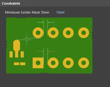
Default constraint for the Minimum Solder Mask Sliver rule
Minimum Solder Mask Sliver - specifies the minimum allowed width of solder mask.
Rule Application
Online DRC and Batch DRC.
Silk To Solder Mask Clearance
Default Rule: required i
This rule checks the clearance between any silkscreen primitive and any solder mask primitive, or exposed copper-layer primitive (exposed through openings in the solder mask). The check ensures that the distance is equal to, or greater than, the value specified in the constraint.
Many manufacturers routinely strip (or 'clip') silkscreen to the mask opening and not just to the copper pad. However, doing so can render silkscreen text unreadable. Being able to catch such occurrences, through DRC, allows you to manipulate offending silkscreen text prior to sending the board to manufacturing.
This design rule replaces the Silkscreen Over Component Pads rule found in previous releases of Altium Designer prior to Altium Designer 13.0. When loading a PCB document from such an earlier release, any defined Silkscreen Over Component Pads rules will automatically be converted to Silk To Solder Mask Clearance rules, with their scopes and constraints set to match legacy behavior. It is advised that you check your rule scopes and associated constraints to ensure accuracy in relation to design requirements.
Constraints
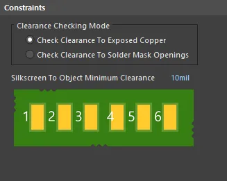
Default constraints for the Silk To Solder Mask Clearance rule
-
Clearance Checking Mode - choose a checking mode for the clearance:
-
Check Clearance To Exposed Copper - in this mode, clearance checking is between silkscreen (Top/Bottom Overlay layer) objects, and copper in component pads which is exposed through openings in the solder mask.
-
Check Clearance To Solder Mask Openings - in this mode, clearance checking is between silkscreen (Top/Bottom Overlay layer) objects, and solder mask openings created by objects that include a solder mask, such as pads, vias, or copper objects with the Solder Mask Expansion option enabled.
-
Silkscreen To Object Minimum Clearance - specifies the minimum permissable clearance between a silkscreen object and either exposed copper, or solder mask openings, depending on the clearance checking mode chosen.
To match the legacy behavior of the old Silkscreen Over Component Pads rule, found in releases of the software prior to Altium Designer 13.0, the Silk To Solder Mask Clearance rule should have its Clearance Checking Mode set to Check Clearance To Exposed Copper, and the full query for one of its rule scopes set to IsPad. As mentioned previously, this is handled automatically when opening older designs.
Rule Application
Online DRC and Batch DRC.
Silk To Silk Clearance
Default Rule: required i
This rule defines the minimum clearance allowed between text and other objects on a silkscreen layer.
Constraints
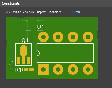
Default constraint for the Silk To Silk Clearance rule
Silk Text to Any Silk Object Clearance - specifies the minimum permissible clearance between any two silkscreen objects.
Rule Application
Online DRC and Batch DRC.
Net Antennae
Default Rule: required i
This rule operates at a net level in the design to flag any open-ended track/arc primitive, or open-ended track/arc that is terminated with a via, and thus forms an antenna.
Constraints
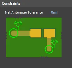
Default constraint for the Net Antennae rule
Net Antennae Tolerance - maximum permissible length for the stub of an open-ended track/arc primitive (or one that terminates in a via).
Rule Application
Online DRC and Batch DRC.
Board Outline Clearance
Default Rule: not required
This rule defines the minimum clearance allowed from design objects that are fabricated, to edges of the board. Either a single clearance value can be specified for all object-to-edge possibilities, or different clearances for different pairings can be defined, through the use of a dedicated Minimum Clearance Matrix. The terms Board Outline and Board Edge are general names used interchangeably to describe the outer edge of the board. The term edge is defined in the table below the image. The Board Outline Clearance design rule checks object-to-edge clearances on the electrical and overlay (silkscreen) layers.
Constraints
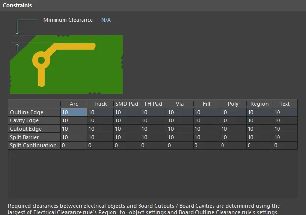
Default constraints for the Board Outline Clearance rule
| Edge Type |
Definition |
| Outline Edge |
The outer-most (exterior) edge of the board |
| Cavity Edge |
The edge of a user-defined cavity |
| Cutout Edge |
The edge of a user-defined cutout |
| Split Barrier |
When a Split Line defines the edge of the board on this layer, this edge is referred to as a Split Line Barrier |
| Split Continuation |
When this layer continues beyond a Split Line, this edge is referred to as a Split Line Continuation (a permeable boundary). To allow an object-kind to cross a Split Continuation, set the clearance value to zero. Zero indicates that for these object-kinds, this is a continuation layer, and the objects are allowed to violate (pass over) the split line. Use this technique to allow routed tracks, for example, to travel across from one Layer Stack Region to another. |
-
Minimum Clearance - the value for the minimum clearance required. A value entered here will be replicated across all cells in the Minimum Clearance Matrix. Conversely, when a different clearance value is entered for one or more object pairings in the matrix, the Minimum Clearance constraint will change to N/A, to reflect that a single clearance value is not being applied across the board.
-
Minimum Clearance Matrix - provides the ability to fine tune clearances between the various object-to-edge clearance combinations in the design.
The default Board Outline Clearance rule for a new PCB document will default to use 10mil for all object-to-edge clearance combinations. When creating a subsequent new rule, the matrix will be populated with the values currently defined for the lowest priority Board Outline Clearance rule.
To allow an object-kind to cross an edge, set the clearance value to zero. Zero indicates to the software that an object-kind is allowed to violate (pass over) this edge type. Use this technique to allow routed tracks, for example, to travel across from one Layer Stack Region to another.
Working with the Clearance Matrix
Definition of clearance values in the matrix can be performed in the following ways:
-
Single cell editing - to change the minimum clearance for a specific object pairing.
-
Multi-cell editing - to change the minimum clearance for multiple object pairings:
-
Use Ctrl+Click, Shift+Click, and Click+Drag to select multiple cells in a column.
-
Use Shift+Click, and Click+Drag to select multiple contiguous cells in a row.
-
Use Click+Drag to select multiple contiguous cells across multiple rows and columns
-
Click on a row header to quickly select all cells in that row.
-
Click on a column header to quickly select all cells in that column.
With the required selection made (either a single cell or multiple cells), making a change to the current value is simply a case of typing the new value required. To submit the newly entered value, either click away on another call, or press Enter. All cells in the selection will be updated with the new value.
To set a single clearance value for all possible object pairings, simply set the required value for the Minimum Clearance constraint. On clicking Enter, this value will be replicated across all applicable cells of the matrix. Alternatively, click the blank grey cell at the top-left of the matrix, or use the Ctrl+A shortcut. This selects all cells in the matrix, ready to accommodate a newly-entered value.
Rule Application
Online DRC, Batch DRC, interactive routing, and autorouting.
