KB: Recess copper away on power plane layer
Created: May 07, 2024 | Updated: July 01, 2024
Starting in version: 18
Up to Current
[Why] Recess copper away on power plane layer from board edge/cutout and via/pad
[What] The pullback from the board edge/cutout is setup in Layer Stack Manager. Clearance with respect to vias and throughhole pads are governed by a rule Plane » Power Plane Clearance
[How] Invoke Design » Layer Stack Manager, select the plane layer, and edit its Pullback distance in Properties panel. Invoke Design » Rules..., expand Design Rules » Plane » Power Plane Clearance, select the catch-all default 'PlaneClearance' to modify or right-click 'New Rule...' to add an additional overriding rule
Solution Details
Pullback from the board edge/cutout:
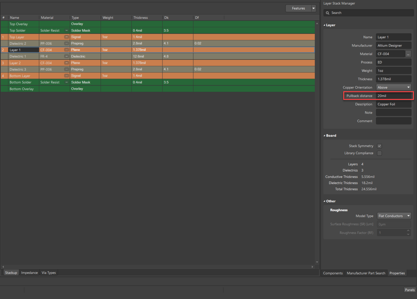
1. Design ► Layer Stack Manager.2. Select the Plane layer in the stack-up
3. Open the Properties panel
4. Edit the Pullback distance within the Properties panel
![](https://www.altium.com/documentation/sites/default/files/wiki_attachments/322969/2633355d2f2906e56afa1d15afb11bc5.jpeg)
Alternatively, the Pullback Distance can also be edited directly within the table (this is the method used for older versions of Altium Designer). To do this:
1. Right-click a Column Header ► Columns
![](https://www.altium.com/documentation/sites/default/files/wiki_attachments/322969/fb1c2124688de7bd51fde9e785cbf69a.jpeg)
2. Within the list, enable the Pullback Distance Column for view
![](https://www.altium.com/documentation/sites/default/files/wiki_attachments/322969/afb09bab206dc112d794d42d0cf4e5f4.jpeg)
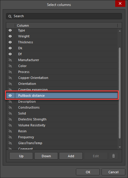
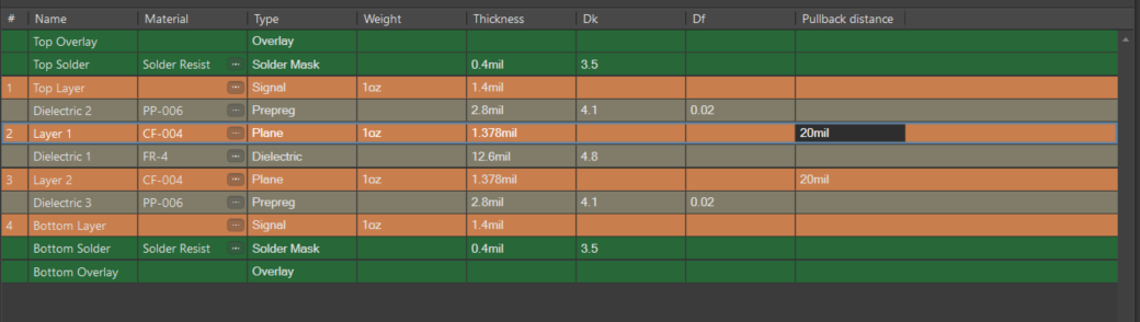
3. The column should now appear on the table, select the Plane layer and edit the column entry.
![](https://www.altium.com/documentation/sites/default/files/wiki_attachments/322969/42b4c92db3f56e7b93a6c50e2a813c8b.jpeg)
Further references:
https://www.altium.com/documentation/altium-designer/pcb-internal-power-split-planes#!pullbacks-and-power-planes
https://www.altium.com/documentation/altium-designer/defining-layer-stack#:~:text=the%20Properties%20panel.-,Pullback%20Distance,-%E2%80%93%20the%20distance%20from
Clearance with respect to vias and throughhole pads:
1. Design ► Rules...2. Expand Design Rules » Plane » Power Plane Clearance
3. Select the catch-all default PlaneClearance to modify or right-click New Rule... to add an additional overriding rule
4. Set the object scope and edit Clearance value on the rule
![image.png](https://www.altium.com/documentation/sites/default/files/wiki_attachments/322969/0ca8dad09a3e055f9da82d9e824af1f8.jpeg)
Further reference:
https://www.altium.com/documentation/altium-designer/pcb-plane-rules#!power_plane_clearance