Power Analyzer by Keysight
The practical performance of a PCB design layout depends on a multitude of factors, many of which can be predicted, to a reasonable degree, through a range of PCB design analysis tools such as post-layout Signal Integrity analysis. What's often neglected, however, or simply relegated to a 'rule of thumb' methodology, is developing the most effective layout design for board's DC Power Delivery systems. This is the judgment applied to the design of a board's copper areas that provide both the DC supply rails to the circuitry and their ground or common return path to the DC supply source. The desired outcome is an efficient design that maintains the integrity of the design's DC power layout.
With modern digital designs featuring high-speed circuitry, multiple devices, densely populated boards, and multiple supply rails, the demands placed on a design's DC power distribution network warrant a more analytical approach to its design. The DC analysis of a Power Delivery Network (PDN), or the results of its DC Power Integrity (PI-DC), is basically aimed at ensuring that adequate copper has been provided in the path from the voltage sources to the loads – in other words, that the planes, traces, and vias on the board are of sufficient size (and characteristics) to meet the power consumption requirements of the devices on the board.
Fortunately, the guesswork can be removed from the assessment of a PCB's power delivery network through the use of a DC Power Integrity (PI-DC) simulation tool, which analyzes a board design's DC performance based on its electrical and physical properties and helps the engineer answer critical design questions, including:
-
Identify and resolve DC voltage and current density issues.
-
Calculate multi-network and return path interactions.
-
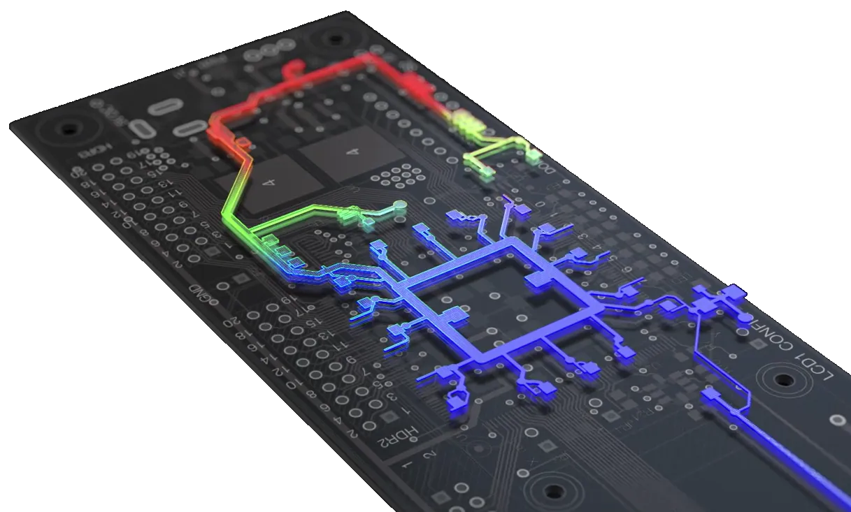
Visualize the voltage and current density distribution and identify hotspots in the PCB editor.
-
Examine the voltage, current density, and via current at any location on the board.
-
Generate a report of the analysis simulation results.
To perform a DC Power Integrity analysis right in the Altium Designer PCB design environment, the go-to solution is the Power Analyzer by Keysight.
The Power Analyzer by Keysight, enabled by Keysight Technologies, integrates directly with Altium Designer to allow PI-DC simulation and analysis of the current PCB project. Rather than relying on simple cross-sectional area calculations to determine the current carrying capacity of the power network, the Power Analyzer first accurately models the copper structures, and then calculates the power delivery voltages and currents across the PCB. With results presented in both visual and tabular form, the engineer can use this feedback and quickly adjust the track widths, copper thicknesses, and via properties to ensure they achieve the integrity of DC power delivery required for their design.
To perform a Power Integrity analysis in Altium, the engineer first creates a hierarchical network of the entire power delivery system, identifying each power and return net, the sources and loads, as well as any series elements present in each section of the power network. Once the network and configuration settings have been defined, the Power Analyzer can examine the entire network.
Configuring the Power Network
The Power Analyzer examines the flow of energy through the copper pathways in the power network. The power network is defined by identifying and configuring the various network elements, including the net, the source, any series components, and the loads. To configure the power network:
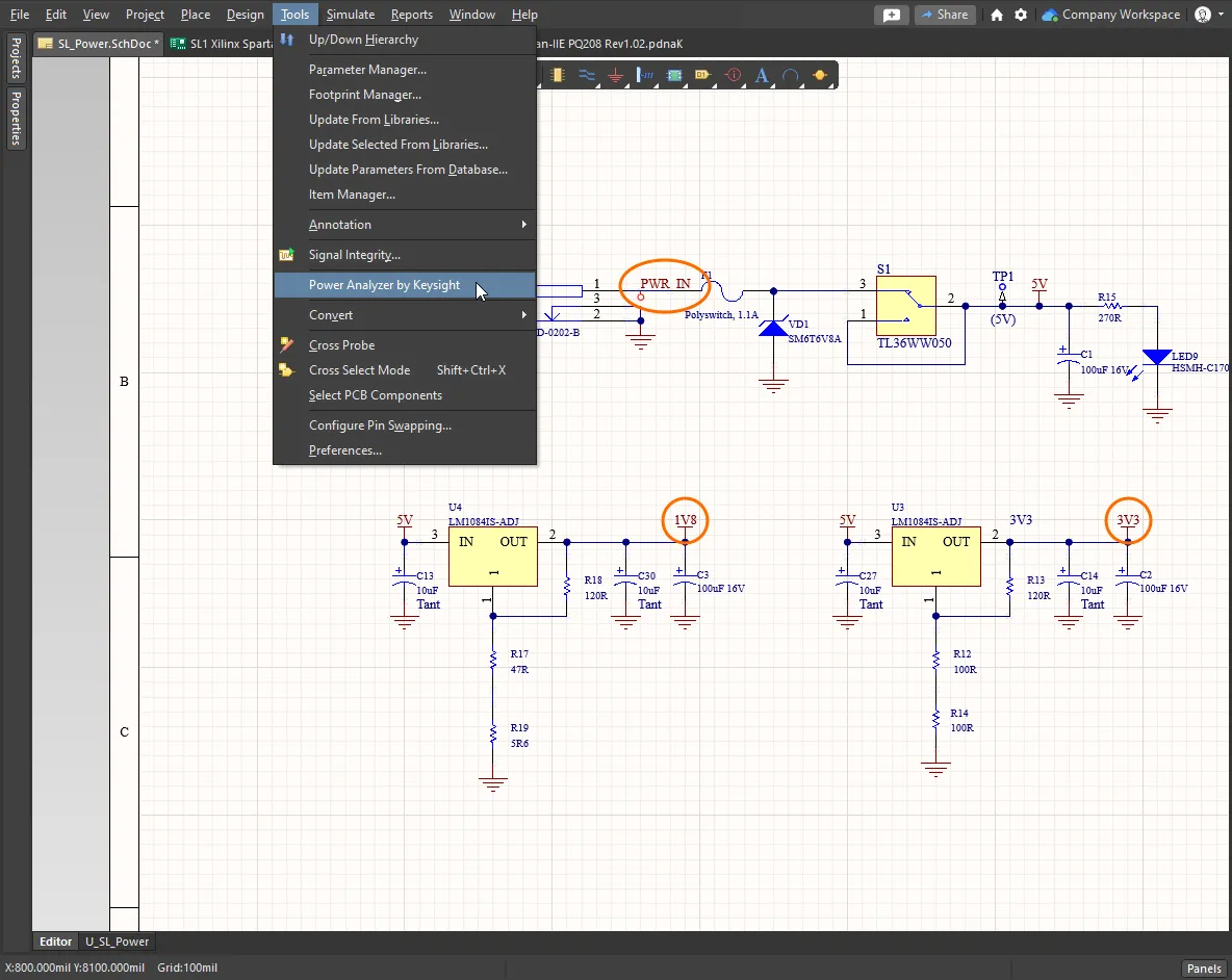
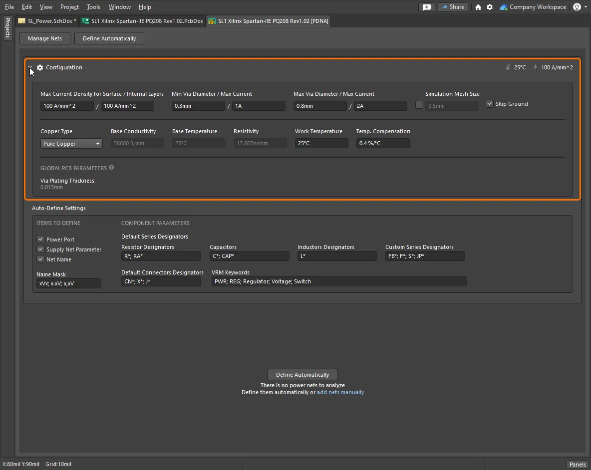
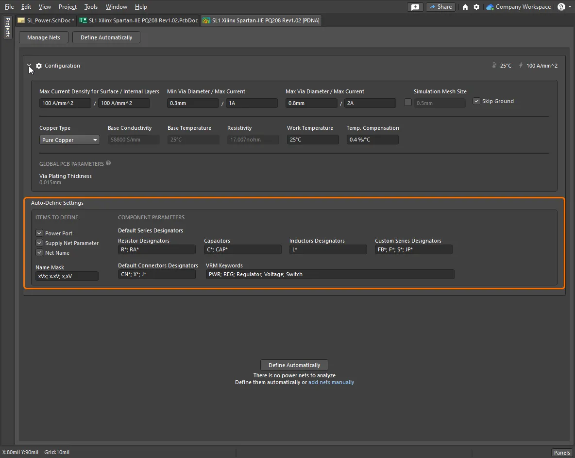
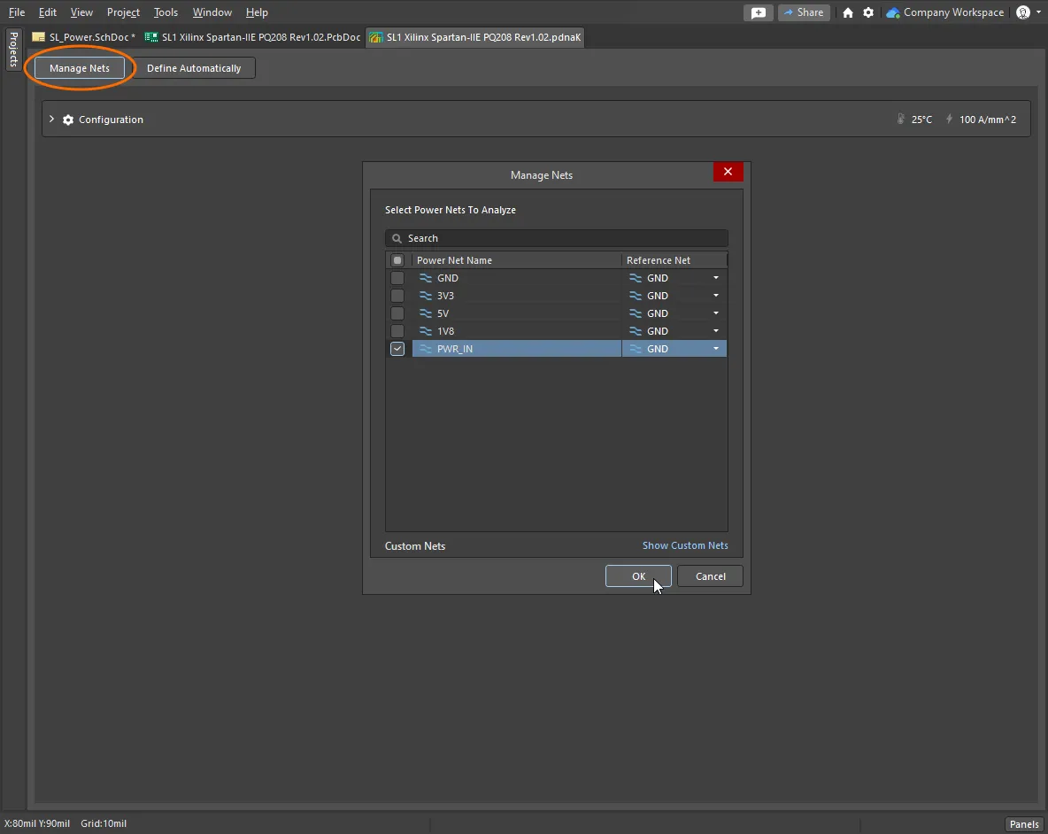
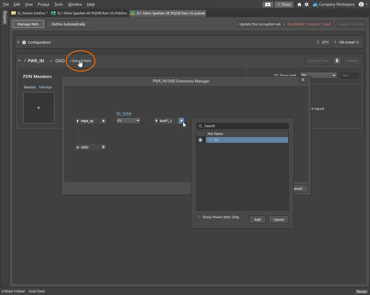
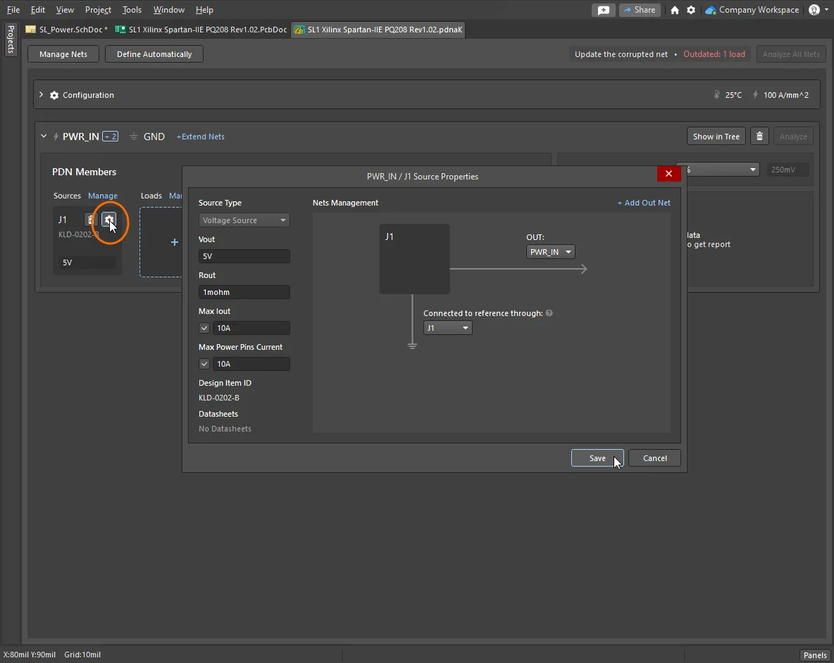
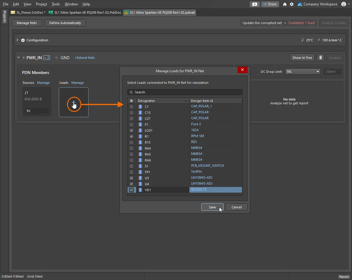
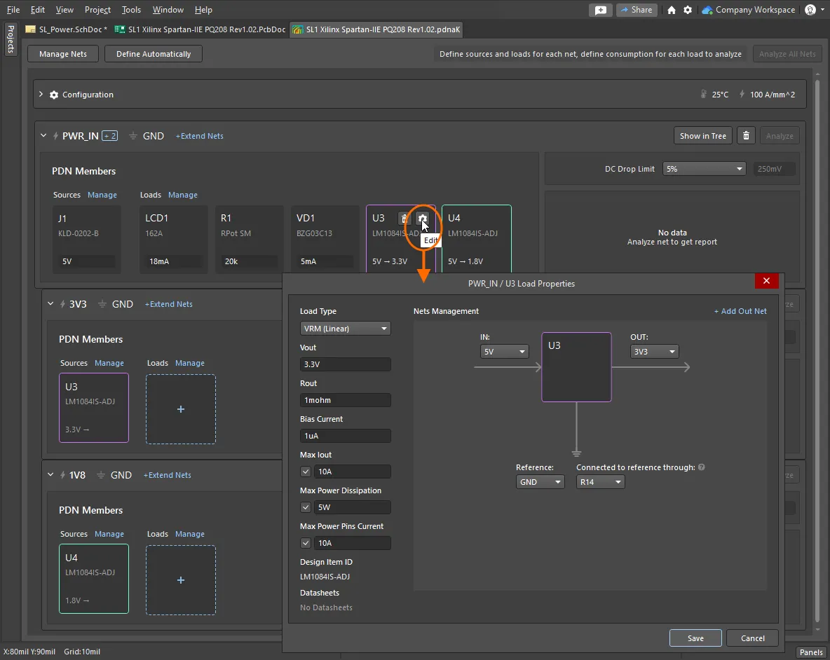
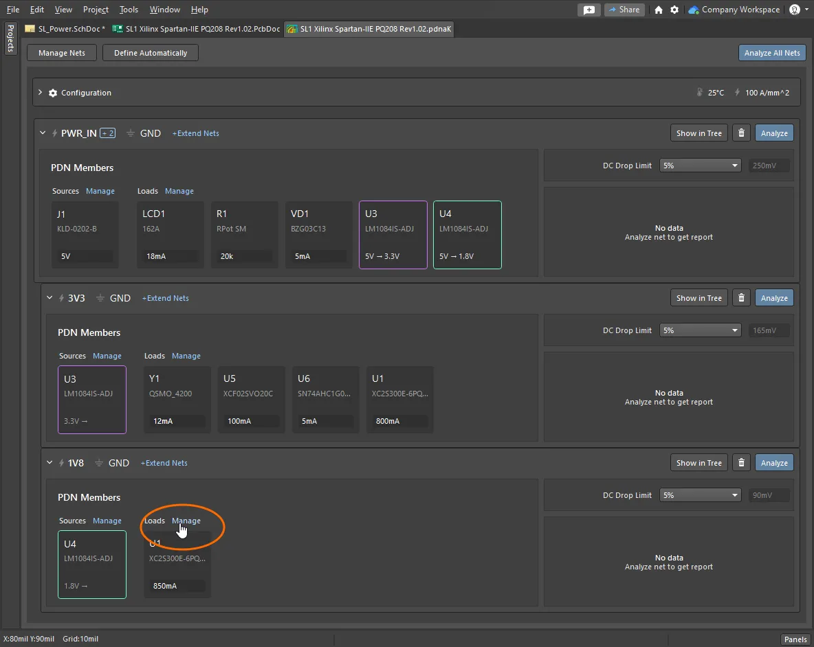
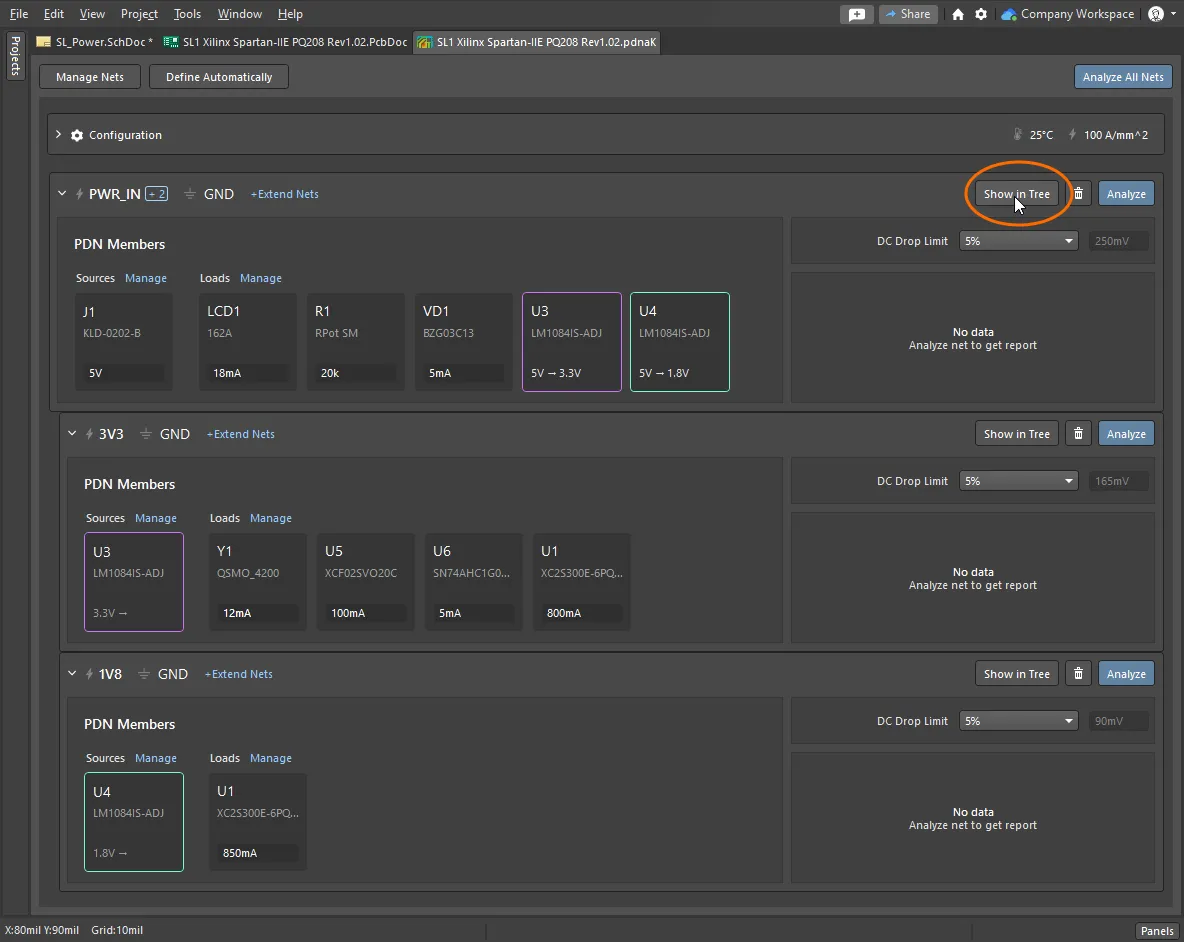
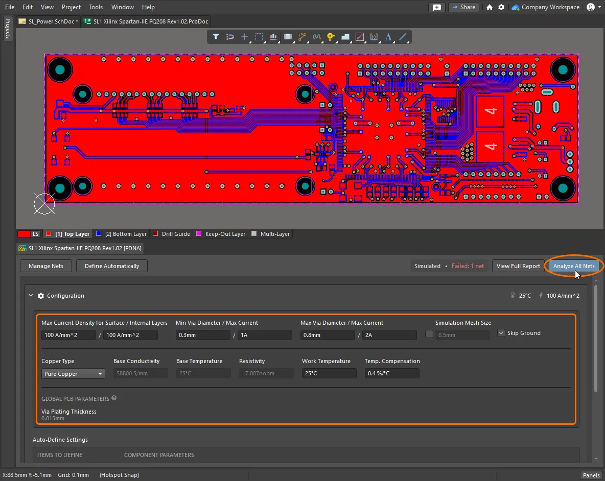
Add an Analysis document to the ProjectAnalysis is configured and run from a Power Analyzer by Keysight document ( Configure the Board PropertiesThe Power Analyzer needs to know the physical properties of the board, such as the allowable current density, the type of copper, the working temperature, and so on. Confirm that the default values defined in the Configuration section of the analyzer document are suitable for your design. Automatic Power Net IdentificationThe Power Analyzer can attempt to identify the power nets automatically. To do this, it needs to know how to identify circuit elements such as voltage regulators, connectors, and series components. As well as using clues such as component designator prefixes, you can also add parameters to certain components to enhance the automatic detection process. Learn more about Configuring the Auto-Define Settings. Choose the Power Net(s)Click Extend the Net(s)If the power net passes through a series component such as a fuse, extend the net and identify the series components and chained nets. Learn more about extending a net. Identify and Configure the SourceEach power net starts from a Source, such as a connector. Enable the source in the Add Source dialog, then click the Gear icon to configure that source. Learn more about identifying and configuring the Source. Identify the LoadsStart with the major current consumers, including the Voltage Regulator Modules (VRMs). Learn more about identifying the Loads. Configure the Loads and VRMsClick the gear icon to open the Load Properties dialog, and configure each load. When a device is configured as a Voltage Regulator Module (VRM), a child power network is automatically created in the hierarchy with that VRM as the source. Identify the Loads in the Child Power NetsEnsure that the major load components are included in each power net. Confirm the Power NetworkClick the Ready for AnalysisCheck the Tree to visually confirm that each power network is complete. To move from one power net to another, click on the Power Analyzer by Keysight link to return to the power net document, and select the Tree for each power net. When this is complete, you're ready to analyze the power network. |
Analyzing the Power Network
Once the Power Networks have been defined, you're ready to analyze the DC power distribution across and through the board.
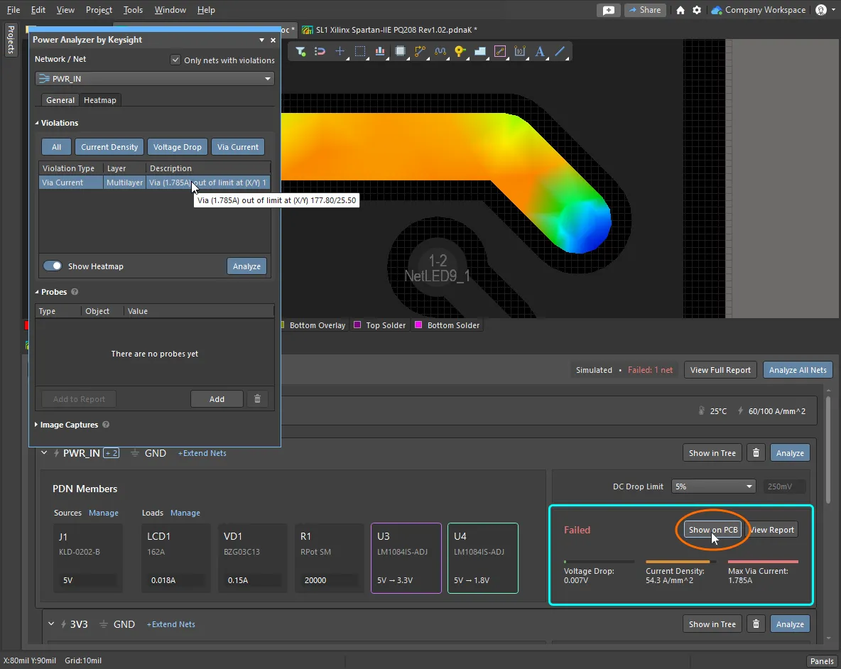
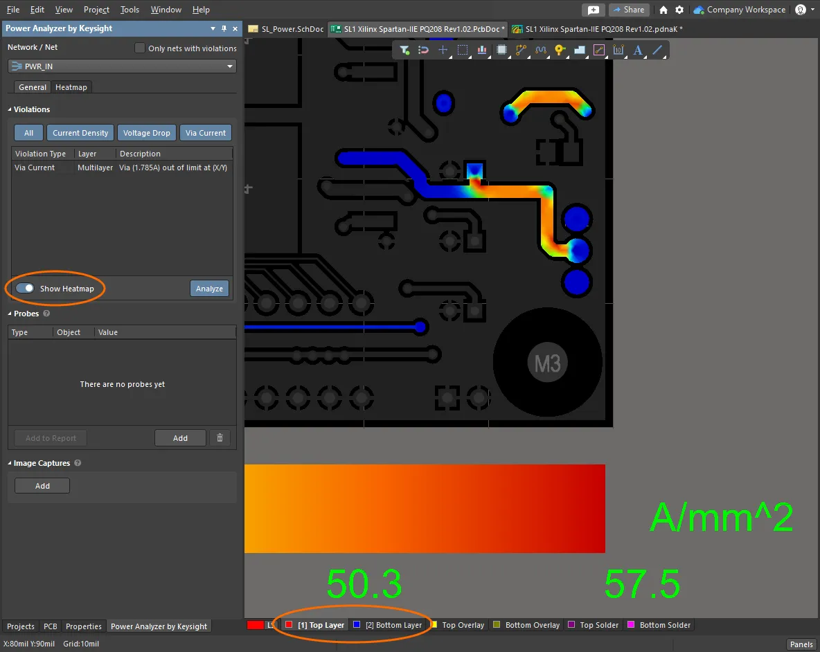
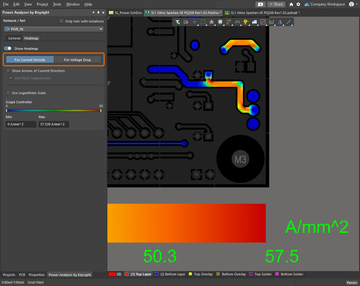
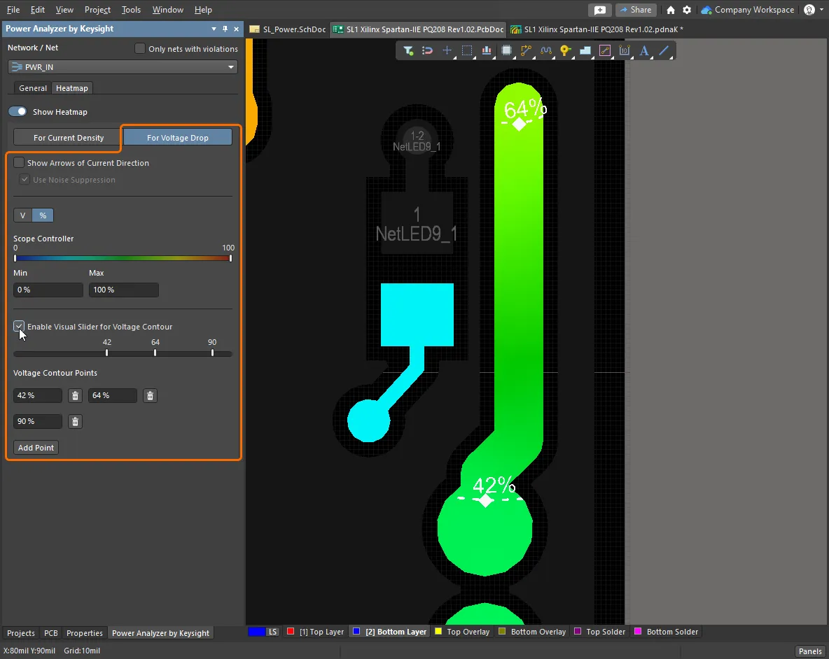
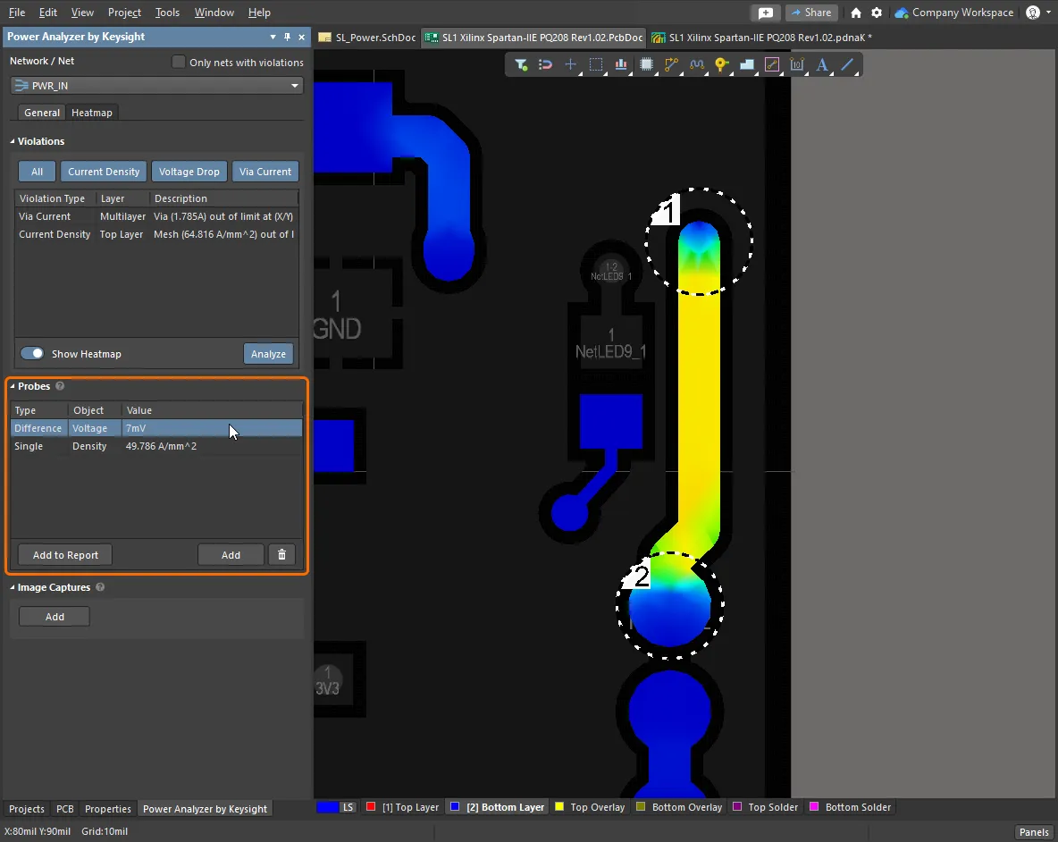
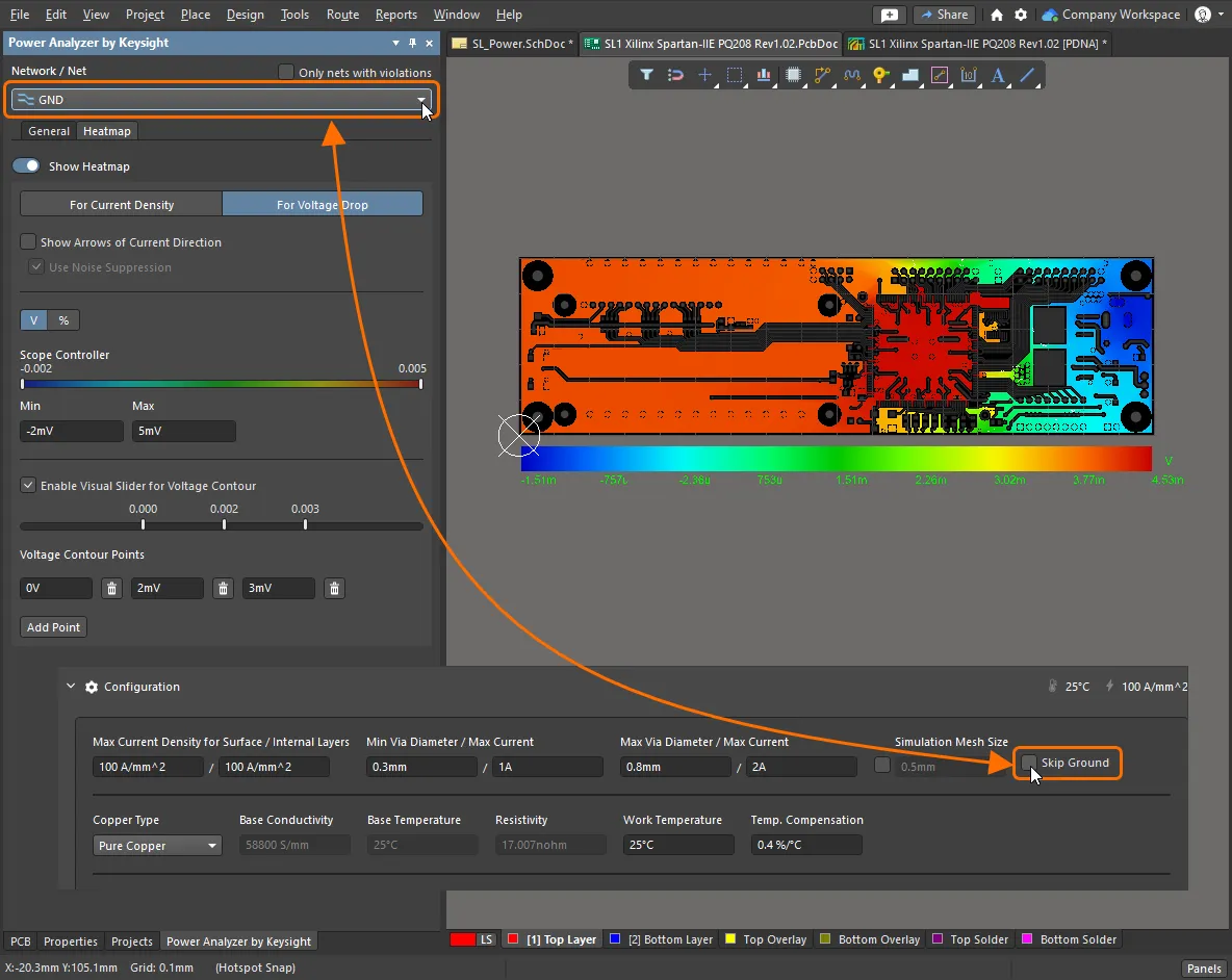
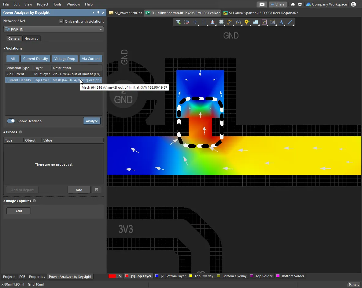
Analyze the Copper StructuresBased on the Configuration settings, when you click the Show on PCBA Summary of the Voltage Drop, Current Density and Max Via Current analysis results are shown as part of the Power Net Definition in the Examine the HeatmapsThe calculated current flow and voltage drops are displayed as Heatmaps, directly in the PCB editor. Use the PCB editor Layer tabs to examine the heatmap on each layer, switch between 2D and 3D PCB view modes with the standard 2 and 3 shortcuts, and click the Show Heatmap button in the Power Analyzer by Keysight panel to switch between the power analysis Heatmaps, and the standard PCB display modes. Explore the Analysis ResultsIn the PCB editor, the power network analysis result you are examining is controlled via the Power Analyzer by Keysight panel. At the top of the panel, select the power network/net whose Heatmap you want to display. Note that if there are violations present in the design, the default is to include Only nets with violations in the dropdown, clear that option to include all power nets in the list. Learn more about the Power Analyzer by Keysight Panel. Switch between Current Density and Voltage DropThe Heatmap displays either the Current Density through the copper or the Voltage Drop across the copper, use the buttons at the top of the Heatmap tab of the panel to select the required mode. A scale for the Heatmap is displayed below the board, automatically scaled for current from Zero to Max Current Density, or for voltage drop from (Voltage - VDrop) to Voltage. Directional arrows indicating current flow can be displayed on the Heatmap, and the Current Density or Voltage Drop scale can be adjusted. Learn more about configuring and controlling the display of the Heatmap. Exploring the Voltage DropThe location of current density hotspots can be directly identified by their color on the heatmap. Because it is calculated as a difference between locations, understanding the voltage drops requires deeper interpretation. To assist in identifying critical locations, use the Enable Visual Slider for Voltage Contour option to display pre-defined contour lines, either as a voltage or as a percentage. Learn more about the Heatmap for Voltage Drop. Probing the ResultsTo take a measurement directly from the Heatmap, place a Probe. Place a single Probe to display the absolute Current or Voltage at that location, or click at a second location to measure the difference between the two Probe points. The type of measurement (V or I) is determined by the current Heatmap mode (Current Density or Voltage Drop). Note that probing the center-point of a thru-hole will always display the Current Density. Learn more about Probes. Examine the Ground Net ResultsBy default, the Ground net is excluded from the Heatmap results. Disable the Skip Ground checkbox in the Configuration section of the |
Interpreting and Reporting the Results
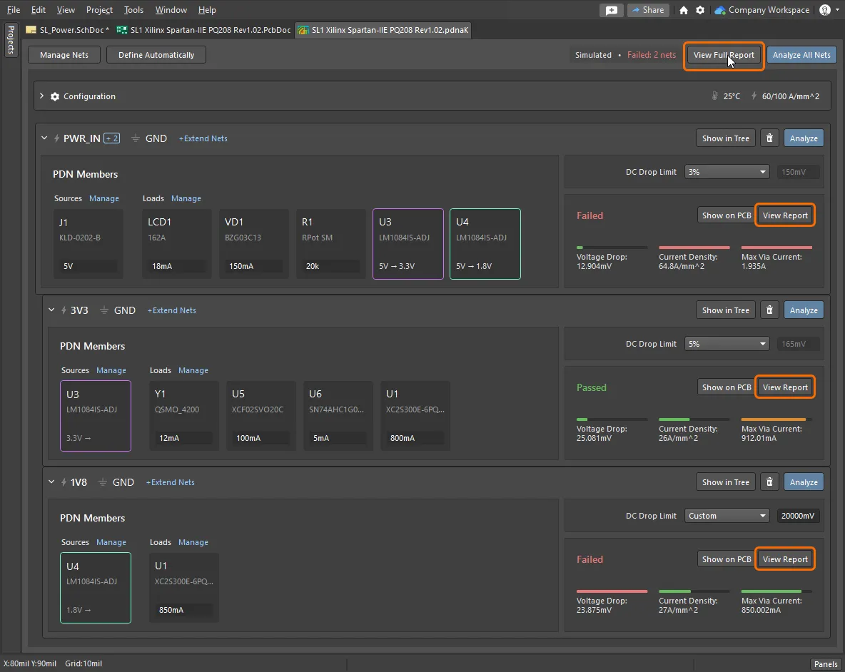
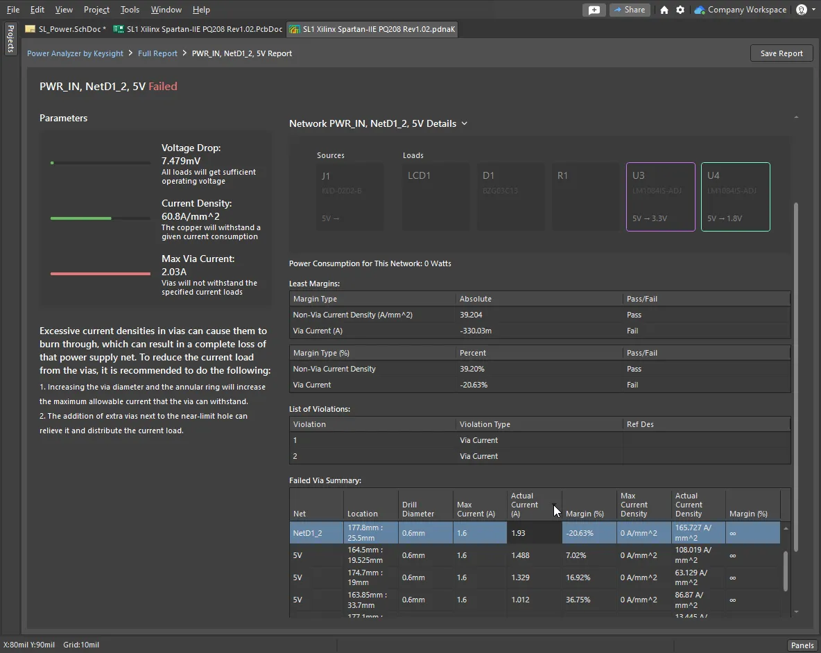
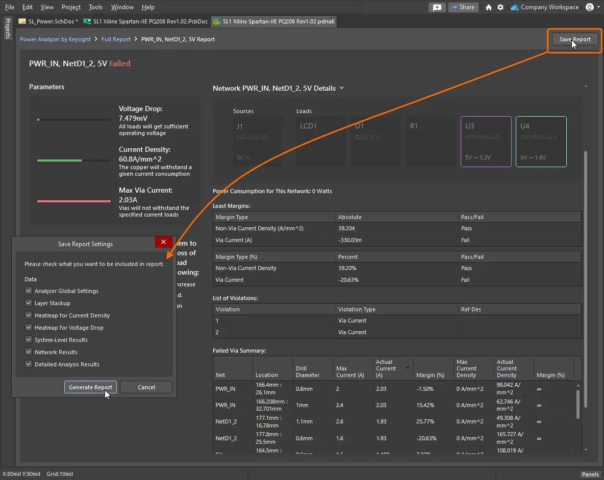
The Power Analyzer provides detailed feedback, directly in the PCB editor. From the Power Analyzer by Keysight panel, violations can quickly be investigated, measurement probes placed, and heatmaps captured as images. To access detailed information about the DC power analysis of your board, a report can be generated. The detailed report opens inside the pdnaK document, and from there, you can save preferred sections into an HTML report file. The report can either be for an individual power net, or the entire power network.
Working with the Interactive Graphical ResultsWorking from the interactive Power Analyzer by Keysight panel, you can quickly identify and examine violations. Generating the ReportTo generate a detailed report, click the Detailed Net Report - ParametersThe Full Report lists all the power nets that have been analyzed; click a Net Name to open the detailed report for that net. The left side of the Net report lists:
Detailed Net Report - ResultsThe right side of the report includes collapsible sections for:
Detailed Net Report - Network DetailsUse the Network Details section to quickly identify potential issues in the design. This section lists:
Save the ReportTo create an HTML report of the analyses, click the
Include Probe Results and Image CapturesImages captured via the |
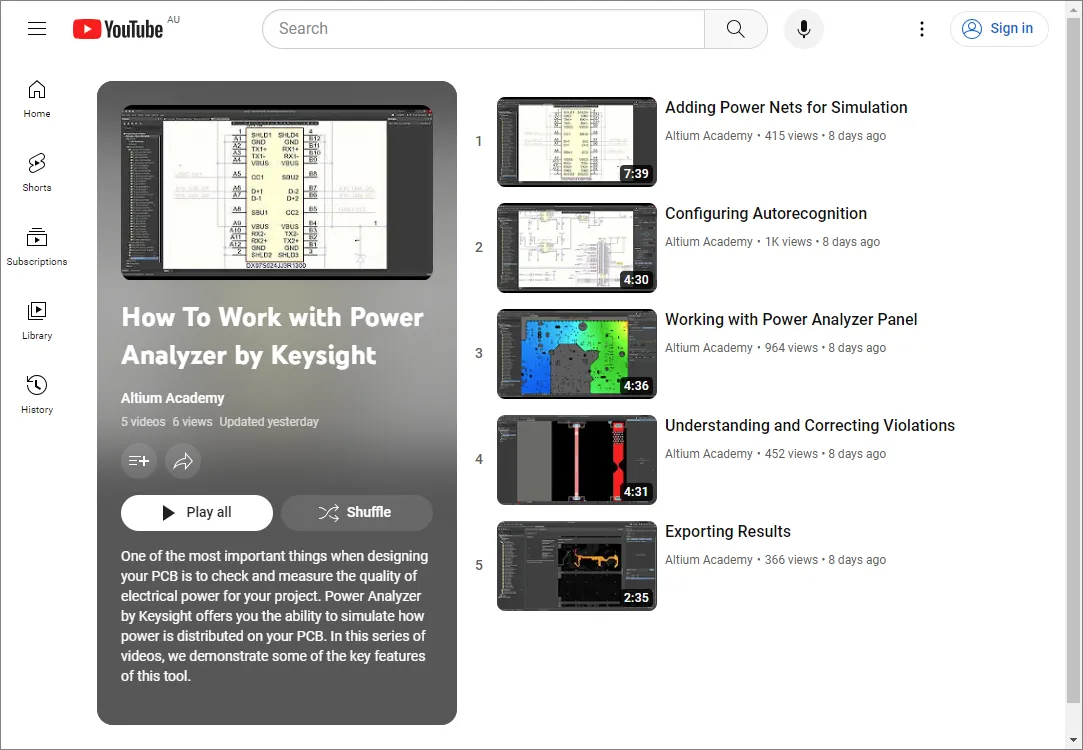
Playlist - How to Work with Power Analyzer by Keysight
It takes time to learn how to work with new design software. If you learn best by watching, then why not check out this video playlist that demonstrates some of the key features of How to Work with Power Analyzer by Keysight.

