When routing a PCB it is fairly common for groups of signals to all need to be routed along the same path, such as for Address and Data busses. One option would be to route each of these signals individually but a much faster option is to route them collectively. The Interactive Multi-Routing command accessed from the main Route menu or the Active Bar allows you to do just that - route multiple nets simultaneously.
Before choosing the command, select the source pad of each net to be included in the route. Shift+click to select individual pads, Ctrl+click and drag to draw a selection rectangle and sub-select multiple child pads in a component.
After launching the command, you will be prompted to click to begin multi-routing. Simply click within the design space at the point where you require to lay down the first set of track segments, then continue routing as required toward your target destination. Use the B (Shift+B) shortcut to decrease (increase) bus spacing in increments of the current grid. Press C to converge bus spacing to the minimum allowed by the applicable routing rules. Use the same shortcuts as for the Interactive Routing to perform other action: cycle through conflict resolution modes, switch routing layers, etc.
It is also possible to enter this mode of routing implicitly, by selecting a group of tracks and dragging their ends (sometimes referred to as Smart Drag). In this mode successive drags can be used to add new segments.
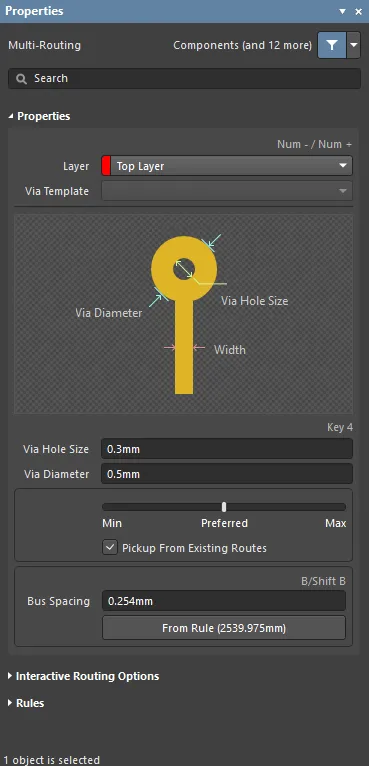
During interactive multi-routing, press Tab to open the Properties panel in its Multi-Routing mode. The following collapsible sections contain information about the options and controls available:
Properties

-
Layer – use the drop-down to specify on which layer the routing is located.
-
Via Template – if the via is associated with a template, the template name is displayed here.
-
Via Hole Size – specify the via hole size or use the 4 shortcut key during routing.
-
Via Diameter – specify the via hole diameter.
-
Width – use the slider bar to specify the width. Farther to the left (Min) signifies that the design rule minimum width defined for the current net will be used. Preferred signifies that the design rule preferred width defined for the current net will be used. Farther to the right (Max) signifies that the design rule maximum width defined for the current net will be used.
-
Pickup From Existing Routes – enable to use the existing track width when routing from a placed track. That is, even if the current routing width is different to the existing track, the existing track width will be adopted when you continue the route from it.
-
Bus Spacing – enter the desired bus spacing or use the Shift+B shortcut.
-
From Rule – click to assign bus spacing based on the existing design rule.
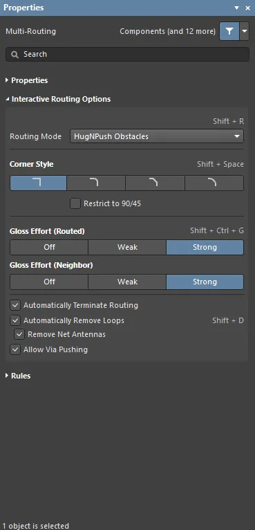
Interactive Routing Options

-
Routing Mode – use the drop-down or use the Shift+R shortcut to cycle through the desired routing modes. The following choices are available:
-
Ignore Obstacles – select to ignore existing objects (routing can be freely placed). Violations are highlighted.
-
Walkaround Obstacles – select to have the Interactive Router route around existing tracks, pads and vias. If this mode cannot walk around an obstacle without causing a violation, an indicator appears to show that the route is blocked.
-
Push Obstacles – select to have the Interactive Router move existing tracks out of the way. This mode can also push vias to make way for the new routing. If this mode cannot push an obstacle without causing a violation, an indicator appears to show that the route is blocked.
-
HugNPush Obstacles – select to have the Interactive Router hug existing tracks, pads, and vias as closely as possible and, where necessary, push obstacles to continue the route. If this mode cannot hug or push an obstacle without causing a violation, an indicator appears to show that the route is blocked.
-
Stop At First Obstacle – in this mode, the routing engine will stop at the first obstacle that gets in the way.
-
AutoRoute Current Layer – select to enable auto-routing only on the current layer.
-
AutoRoute MultiLayer – select to enable auto-routing on multiple layers.
-
Corner Style – select the desired routing corner style or use the Shift+Spacebar shortcut to cycle through the corner styles.
-
Restrict to 90/45 – enable to restrict the routing to 90 degrees and 45 degrees only.
-
Gloss Effort (Routed) – select the desired gloss level directly from the panel or use the Shift+Ctrl+G shortcut to cycle through the following choices:
-
Off – in this mode, glossing is essentially disabled. Note, however, that cleanup is still run after routing/dragging occurs to eliminate, for example, overlapping track segments. This mode is typically useful at the end stage of board layout when the ultimate level of fine-tuning is required (for example, when manually dragging tracks, cleaning pad entries, etc.).
-
Weak – in this mode, a low level of glossing is applied with the Interactive Router considering only those tracks directly connected to or in the area of the tracks that you are currently routing (or tracks/vias being dragged). This mode of glossing is typically useful for fine-tuning track layout or when dealing with critical traces.
-
Strong – in this mode, a high level of glossing is applied with the Interactive Router looking for shortest paths, smoothing out tracks, etc. This mode of glossing is typically useful in the early stages of the layout process when the aim is to get a good amount of the board routed quickly.
-
Gloss Effort (Neighbor) – select the desired gloss level to apply to traces being pushed by the net currently being routed directly from the panel through the following choices:
-
Off – in this mode, glossing is essentially disabled. Note, however, that cleanup is still run after routing/dragging occurs to eliminate, for example, overlapping track segments. This mode is typically useful at the end stage of board layout when the ultimate level of fine-tuning is required (for example, when manually dragging tracks, cleaning pad entries, etc.).
-
Weak – in this mode, a low level of glossing is applied with the Interactive Router considering only those tracks directly connected to or in the area of the tracks that you are currently routing (or tracks/vias being dragged). This mode of glossing is typically useful for fine-tuning track layout or when dealing with critical traces.
-
Strong – in this mode, a high level of glossing is applied with the Interactive Router looking for shortest paths, smoothing out tracks, etc. This mode of glossing is typically useful in the early stages of the layout process when the aim is to get a good amount of the board routed quickly.
-
Automatically Terminate Routing – when enabled, when you complete a route to the target pad, the routing tool does not continue in routing mode from the target pad but rather resets and is ready for you to click on the next source pad from which to route. If this option is disabled, after you route to the target pad, the tool will remain in routing mode and use the previous target pad as the source for the next route.
-
Automatically Remove Loops – enable to automatically remove any redundant loops that are created during manual routing. This allows you to re-route a connection without having to manually remove redundant tracks. However, there are times when you need to route nets such as power nets and you need loops – you can toggle this option for a selected net by using the Shift+D shortcut to override this global setting for the same net.
-
Remove Net Antennas – enable this option to remove any track or arc end that is not connected to any other primitive and forms an antenna.
-
Allow Via Pushing – check this option to allow pushing a Via when in Push Obstacles or HugNPush Obstacles mode.
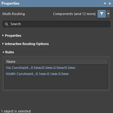
Rules

Constraints defined by the applicable design rules will be listed under the Rules section of the Properties panel.
-
Via Constaint – click to open the Edit PCB Rule dialog to view/edit the rule.
-
Width Constraint – click to open the Edit PCB Rule dialog to view/edit the rule.