Board level annotation is the process of annotating the compiled components (the physical view of your components) of your design through the Schematic editor. It allows you to either name your components based on a number of naming schemes or specify custom names.
While it can be used in any design, it is especially useful for multi-channel designs and/or designs that incorporate device sheets, where the designators cannot be edited on the device sheet itself. In this way, the entire design can be re-annotated without actually modifying the original device sheet(s). Board level annotation also resolves any conflicting annotation problems that may occur due to duplicate designators across a project and stores its changes in a *.Annotation text file. It includes additional keywords for customizing naming schemes and allows them to be applied to all or only a select range of parts.
Board level annotation gives you complete control over the annotation in your project, with annotation settings saved in a *.Annotation text file displayed under the Settings\Annotation Documents sub-folder in the Projects panel. Altium Designer manages annotation files automatically.
You can choose to name all of the components in your project, name selected components, or name only those components that are not designated.
Configuring Board Level Annotation
To annotate the compiled components in your project through the Schematic editor:
-
Ensure that the components have been annotated at the schematic level so that the schematic source data, including packaged options for multi-part components, is available as input for board level annotation.
-
Select Tools » Annotation » Board Level Annotate (shortcut Ctrl+L), which opens the Board Level Annotate dialog.

The Board Level Annotate dialog displays all of the schematic documents in your project.
This dialog is comprised of two main regions:
-
Filter Options - for filtering and setting the scope of annotation.
-
Proposed Change List - the proposed changes to be applied, based on your configured annotation options. Changes are applied through an Engineering Change Order (ECO).
Board Level Annotate - Filter Options
The left side of the Board Level Annotate dialog allows you to control the scope of annotation at the sheet, channel and part level. The columns in the Filter Options region do not change.
-
Schematic Sheet - this column lists all of the schematic documents in the project. A schematic document may be listed more than once if the design includes multiple channels.
-
Channel Name - this column lists all of the relevant channels in the design. If there are no channels in the design, this column will be populated with the schematic sheet name.
-
Enabled - check this box to include this schematic sheet for a specific channel in this board level annotation. Uncheck the box to exclude this sheet from board level annotation.
-
Annotation Scope - choose from the following to set the scope for the parts to be annotated:
-
All - all parts in the schematic sheet will be annotated.
-
Ignore Selected Parts - all parts except those selected will be annotated.
-
Only Selected Parts - only the parts selected will be annotated.
Parts to be included or excluded in board level annotation need to be selected before opening the Board Level Annotate dialog.
Board Level Annotate - Proposed Change List
The right side of the dialog displays Schematic Source Components (highlighted in pink) and Calculated Design Data (highlighted in green) used in the current naming scheme (whether it is the default name for compiled components or the applied naming scheme), apply a Naming Scheme, and view the resulting PCB Component Instance.
-
Local Index - the index you have specified following the alphabetical prefix extracted from the schematic level designator. For example, if the schematic level designator is
R13, the Local Index is 13.
-
Calculated Design Data - upon first opening the dialog, the Calculated Design Data section displays the Room Name column, which corresponds to the default Annotate Option selected. Once a board level annotation has been performed, the columns displayed in Calculated Design Data represent the keywords selected in the naming scheme for annotation in the Annotate Options. These columns are updated dynamically based on your selection. For example, if you select the Naming Scheme to be $GlobalIndex.$SheetDesignator, the columns displayed will be Global Index and Sheet Designator.
-
Naming Scheme - check the box to enable the Naming Scheme for this component. Uncheck the box to disable the Naming Scheme for this component. Note that when this field is unchecked, the PCB Component Instance column can be edited so you can specify a custom designator for your component.
-
PCB Component Instance - this column displays the proposed designator. This field is dictated by either the Naming Scheme selected or a custom value that can only be specified when the Naming Scheme field is unchecked. The custom name can contain any combination of alphanumeric and non-alphanumeric characters.
The following buttons are located beneath the Proposed Change List:
Alternatively, if you want to specify a custom name for all or a particular component, uncheck the Apply box under the Naming Scheme column (in the Board Level Annotate dialog) to disable the Naming Scheme for selected components and edit the PCB Component Instance column.
Options and Controls of the Board Level Annotation Options Dialog
Name Scheme
Use the drop-down to select a predefined naming scheme or define your own naming scheme using valid keywords. You can select any combination of valid keywords in any order and any non-alphanumeric characters to separate keywords (for example, "_", "*", ".", and "@"). Choose from the keywords tabulated below.
Keyword
|
Definition
|
$RoomName
|
Name of the associated room as determined by the style chosen in the Room Name Options
|
$ComponentPrefix
|
Component logical designator prefix (e.g., U for U1)
|
$ComponentIndex
|
Component logical designator index (e.g., 1 for U1)
|
$ChannelPrefix
|
Logical sheet symbol designator
|
$ChannelIndex
|
Index specified to distinguish between different channels.
|
$ChannelAlpha
|
Channel index expressed as an alpha character. This format is useful only if your design contains less than 26 channels in total, or if you are using a hierarchical designator format.
|
$SheetDesignator
|
Designator assigned to the sheet symbol
|
$SheetNumber
|
The sheet number assigned to the sheet. If compiled sheets have been annotated, this information will be used.
|
$DocumentNumber
|
The Document Number specified in Document Options.
|
$GlobalIndex
|
User-defined index. You can specify the order, Start Index and/or a suffix in the Global Index Options for each schematic document. Global Index is calculated for all non-designated components. If you add new components after you have performed a board level annotation, these components will be annotated with a new Global Index and the existing components will retain their Global Index. To recalculate the Global Index for all components, click Reset All first.
|
The following options and controls vary depending on the document being annotated.
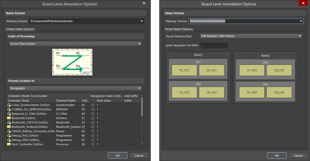
Global Index Options
-
Order of Processing - use the drop-down to define the processing order desired. The graphical representation will dynamically change according to your selection:
-
Up Then Across
-
Down Then Across
-
Across Then Up
-
Across Then Down
-
Process Location of - use the drop-down to select the type of information to process, e.g., Designator.
-
Schematic Sheets To Annotate - a list of the schematic sheets. Click on a column heading to sort the list by that subject. Listed information includes:
-
Schematic Sheet - the name of the schematic sheet.
-
Channel Name - the name of the channel.
-
Order - the order in which the listed item will be annotated.
-
Designator Index Control - enable the checkbox to enable designator index control of the listed schematic sheet.
-
Start Index - click in this column and use the up/down arrow keys to select the start index. You can also enter the desired index number.
-
Add Suffix - enter the desired suffix.
Right-click Menu
The right-click menu in the bottom grid area includes the following commands:
-
Enable Designator Index Control - select to check all Designator Index Control checkboxes.
-
Disable Designator Index Control - select to uncheck all Designator Index Control checkboxes.
-
Order Alphabetically - select to sort the listed schematic sheets alphabetically.
-
Order by Project Order - select to sort the listed schematic sheets by project order.
Room Name Options
-
Annotate - click on the drop-down to choose Annotate Undesignated, Annotate All or Annotate Selected. Once chosen, the Proposed Change List will be updated with the designator to be annotated to each applicable component.
-
Reset All - click to reset all of the designators to the default names for compiled components. After components have been reset, the Prefix column will display a component icon with a question mark ( ) to show that the component is now undesignated.
-
Back Annotate - use to synchronize changes from your PCB design to the compiled documents in the Schematic editor. After clicking the Back Annotate button, a File Explorer dialog opens in which you can choose the file for back annotation. Back annotation for board level annotation performs the same way as it does for schematic level annotation. Learn more about generating the Was-Is file.
Note that back annotation is a legacy feature, therefore, it is recommended to use Design » Update to push annotation changes from the PCB back to the schematic.
To complete board level annotation:
-
Click the Accept Changes (Create ECO) button. The Engineering Change Order dialog opens in which you can validate, report and execute the ECO.
-
Click the Execute Changes button and then the Close button to execute board level annotation.
-
Click the Close button on the Board Level Annotate dialog. The *.Annotation file will be updated, and you can view your board level annotation in your documents. To complete board level annotation, synchronize the schematic documents with your PCB documents by selecting Update PCB Document <Filename> from the Design menu.
Board Level Annotation and Device Sheets
Device sheets are portable and can be reused between designs. In most cases, the names of the components in device sheets are limited to the scope of that sheet and require board level annotation in order to be incorporated into the design in which they are placed.
Board level annotation is relevant to device sheets because different device sheets included in one project can contain duplicate designators, resulting in compilation errors. Board level annotation can resolve any conflicting naming with the changes saved to an *.Annotation file displayed under the Settings - Annotation Documents sub-folder.
Default Names for Compiled Components
Default names are required to distinguish between the different instances of the physical representations of components. These default names are displayed in your documents and are used if you have not performed a board level annotation to annotate your compiled (physical) components. When you first launch the Board Level Annotate dialog, the default names are populated in the PCB Component Instance column.
Default naming of compiled components is also applicable for multi-channel designs that reference the same sheet in a project multiple times. This is done by either placing multiple sheet symbols that reference the same sheet in the schematic document or by including the Repeat keyword in the designator of a sheet symbol to instantiate a sheet multiple times.
While this makes it easy to repeat circuitry, it also presents a challenge in terms of annotation. In a multi-channel design, there can only be one logical instance of each component with its own unique designator, no matter how many "copies" of it exist on the PCB. The Multi-Channel tab of the Project Options dialog (Project » Project Options) ensures that each channel is uniquely annotated with a default name based on Room Naming Style and Component Naming Designator Format.
Multi-Channel Tab
Rooms are regions that assist in the placement and annotation of components in multi-channel designs. More specifically, a channel on the schematic is an instance of a repeated sheet, and on the PCB, each channel is represented by a room. Once components have been assigned to a room, they move when the room is moved, allowing separate channels to be easily controlled and identified.
Rooms play an important role in channel designations, ensuring unique names.
Logical designators are assigned to the components on the Editor tab. Physical designators are assigned to the components when they are placed in the PCB design or when you have performed a board level annotation. In multi-channel designs, the logical designators for repeated channel components may be the same, but each component must have a unique physical designator in the PCB design. This can be accomplished by appending the Room Name to the component name, as shown in the Component Naming field below.
The Multi-Channel tab of the Project Options dialog allows you to specify the Room Naming Style and the Component Naming Designator Format for your designs. By controlling the multi-channel designator format in this dialog, you control the mapping from the single logical component on the Editor tab to the multiple physical instances on the PCB. The tab is essentially divided into two areas – Room Naming and Component Naming.

The Multi-Channel tab allows for flexible default naming formats in multi-channel designs.
Room Naming
Use the Room Naming Style drop-down to define the naming format required for the rooms in your design. These rooms are created by default when you update the project schematics to the PCB. There are five styles available — two flat and three hierarchical.
Flat Room Name Formats
|
Hierarchical Room Name Formats
|
Flat Numeric With Names
|
Numeric Name Path
|
Flat Alpha With Names
|
Alpha Name Path
|
Mixed Name Path
|
Hierarchical room names are formed by concatenating all channelized sheet symbol designators (ChannelPrefix + ChannelIndex) in the relevant channel path hierarchy.
As you select a room naming style from the list, the graphical representation is dynamically updated to reflect the naming convention that will appear in the design. The larger cross-hatch regions represent the upper-level channels (or banks), and the shaded regions within represent the lower-level channels. When the design is compiled, a room is created for each sheet in the design, including each bank and each lower-level channel.
Use the Level Separator for Paths field to specify the required character/symbol to separate the path information when using the hierarchical naming styles. There are no restrictions on the character used for the level separator, however, a single non-alphanumeric character is easier to read.
Component Naming
There are several designator formats available for naming components. You can choose a format or define your own using valid keywords. Define the Component Naming format by selecting from the Designator Format drop-down list. There are eight predefined formats — five flat and three that can be used in a hierarchical context:
Flat Designator Formats
|
$Component$ChannelAlpha
|
$Component_$ChannelPrefix$ChannelAlpha
|
$Component_$ChannelIndex
|
$Component_$ChannelPrefix$ChannelIndex
|
$ComponentPrefix_$ChannelIndex_$ComponentIndex
|
Hierarchical Designator Formats
|
$Component_$RoomName
|
$RoomName_$Component
|
$ComponentPrefix_$RoomName_$ComponentIndex
|
The flat designator formats name each component designator in a linear progression, starting from the first channel and avoiding the duplication of designators. The hierarchical designator formats include the Room Name in the designator for a component. If the chosen Room Naming Style is one of the two possible flat styles, then the style for the component designator will also be flat. However, if a hierarchical style has been chosen for the Room Naming Style, the component designator will also be hierarchical since the path information will be included in the format.
Defining Your Own Designator Format
You can define your own component designator format by typing directly into the Designator Format field using valid keywords. Select from any combination of the following keywords to construct the format string.
Keyword
|
Definition
|
$RoomName
|
Name of the associated room as determined by the style chosen in the Room Naming Style field
|
$Component
|
Component logical designator (e.g., U1)
|
$ComponentPrefix
|
Component logical designator prefix (e.g., U for U1)
|
$ComponentIndex
|
Component logical designator index (e.g., 1 for U1)
|
$ChannelPrefix
|
Logical sheet symbol designator
|
$ChannelIndex
|
Index specified to distinguish between different channels
|
$ChannelAlpha
|
Channel index expressed as an alpha character. This format is useful only if the design contains less than 26 channels total or if you are using a hierarchical designator format.
|
The Room Naming Style is only relevant for component naming if the $RoomName string is included in the Designator Format.
Displaying Physical Names in Your Documents
Your design is constructed on the Editor tab. Compiled documents (physical representations of your design) are visible and can be accessed by clicking on the compiled document tab located at the bottom of the schematic document in the design space.

Examples of design space tabs
You can specify display preferences for the physical names in compiled documents on the Schematic - Compiler page of the Preferences dialog. In the Compiled Names Expansion region, select to expand the compiled (physical) names of Designators, Net Labels, Ports, Sheet Number, and/or Document Number.
You can also use the associated drop-down to select how the objects are displayed. Choices include Never display superscript (expanded names are never displayed), Always display superscript (expanded names are always displayed), or Display superscript if necessary (expanded names are only displayed if they are different from the source).
The superscript options apply to both the Editor tab and the compiled document tabs. In the Editor tab, the compiled names are in superscript; in the compiled document tab, the logical name (the name in the Editor tab) is displayed in superscript.
Use the Design » Update PCB Document command to initiate a transfer process that automatically creates a component class for each schematic sheet in the design, a room for each component class, and also groups the components in each class in their room ready for placement.
