Parent page: Working with Views
A Draftsman Board Assembly View is an automated graphic composite of the active PCB project's board outline, cutouts, holes, and component graphics with additional notation. Its drawing representation, included information and data sources are all configurable in the Properties panel.

A placed board Assembly View can be moved, scaled and viewed from different sides.
An Assembly View for the nominated source project PCB is placed in a document by selecting the  button on the Active Bar, or via the Place menu options. After launching the command, drawing data is retrieved from the source PCB file, the cursor will change to a cross-hair and the rendered Board Assembly View is attached to the cursor. Move the cursor to the desired position then click to confirm the placement.
Note that drawing data is retrieved from the PCB document specified in the Source section of the Properties panel when in Document Options mode. To change the panel to that mode, deselect all objects in the design space (click in free space).
Both the position and size of placed Board Assembly View may be graphically modified.
A selected Board Assembly View will show a node handle at the top right of the selection outline, which can be dragged to a new location to modify the view's size. To move a Board Assembly View, drag and drop it to a new location.
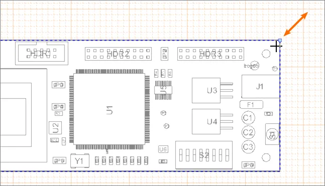
Drag a selected Assembly View's resize node to change its scale.
Components
The Board Assembly View's component graphics are automatically generated and take data on a priority basis from several sources, such as:
- The projection of a board component's three-dimensional model (3D model) – used by default.
- A component's silkscreen graphic taken from the Top/Bottom Overlay layer – used when a 3D model is not available.
- A graphic of the component's dimensions derived from its contact pads (its Bounding Box) – used when both a 3D models and screen overlay are not available.
-
A component graphic on the Assembly Component Layer Pair specified in the PCB design, under the Layers & Colors tab of the View Configuration panel – the layer pair containing component data is set to the Assembly Layer Type in the associated Edit Layers dialog.
Note that the automatic generation of a Board Assembly View does not rely on the availability of an additional board assembly layer (for example, Top/Bottom Assembly), so this mode is an option.
Use the Component Display Properties section of the Properties panel to set the visibility, designator attributes and graphic style of all components shown on the Board Assembly View. Alternatively, select a specific component on the Assembly drawing itself to set only its graphic options in the Component Display Properties section. Multiple components may be selected in order to adjust properties across various components.
For access to all component display attributes, including component Footprints, Classes and any associated Parameters, select the panel's  button to open the Component Display Properties dialog, where component properties may be changed individually, in groups or through multiple selection.
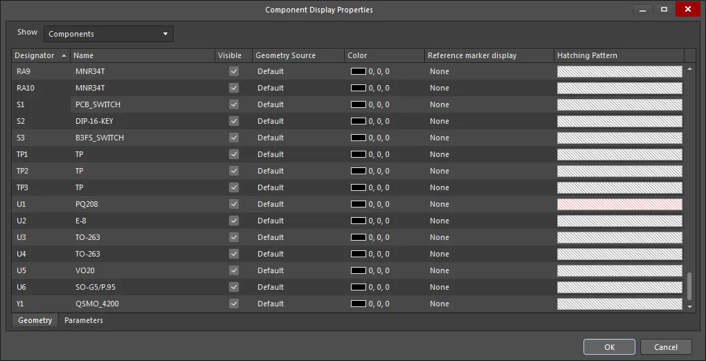
Options and Controls of the Component Display Properties Dialog
Geometry Tab
 The Geometry tab of the Component Display Properties dialog
- Show menu – use the drop-down to select in which grouping format the component properties will be displayed: Components, Classes, Footprints, or BOM Items.
Columns
- Items – the BOM entry (item) number. Applies when Show is set to
BOM Items.
- Designator – the component entry's Designator parameter value. Applies when Show is set to
Components.
- Name – the name of the entry, based on the data type selected by the Show option.
- Components option – component Footprint name.
- Classes option – name of collective component Class, as shown in the Components mode of the PCB panel.
- Footprints option – Footprint name.
- BOM Items option – component Description parameter.
- Visible – toggle the visibility of a component's graphics, based on the Show setting. When Show is set to
Classes for example, the Visible option will toggle the graphics display of all components that fall under the indicated Class.
- Geometry Source – use the drop-down to select the data source used for rendering the component's graphics:
- Default – the component graphics will be taken in order of priority from the options below.
- BodyProjection – the component's 3D model, if available.
- BodyProjectionSimple - the component's simple 3D body.
- SilkScreen – the silk screen printing layer.
- BoundingBox – dimensions derived from the component's contact pads.
- AssemblyDrawing – the component graphic on the Assembly Component Layer Pair specified in the PCB design, under the Layers & Colors tab of the View Configuration panel – the layer pair containing component data is set to the
Assembly Layer Type in the associated Edit Layers dialog.
- Color – the color of the component graphics. Select and use the drop down menu options to specify an alternative standard color, or one selected from a RGB or HSB color palette.
- Reference marker display – use the drop-down to select the display of the reference marker. Choices include: None or InsideContour (a dot indicating pin 1).
- Hatching Pattern – select a pattern entry and use its associated
 button to open the Fill Style dialog. In the dialog, select the visual pattern and color used to render the component's profile, such as when it is displayed in a board Section View.
Parameters Tab
 The Parameters tab of the Component Display Properties dialog
- Show menu – use the drop-down to select in which grouping format the component properties will be displayed: Components, Classes, Footprints, or BOM Items.
- Add Parameter – click the
 to add a new parameter column group (Parameter [n]). Use the Parameter Name drop down to select from the available parameters for the component entry.
Columns
- Items – the BOM entry (item) number. Applies when Show is set to
BOM Items.
- Designator – the component entry's Designator parameter value. Applies when Show is set to
Components.
- Name – the name of the entry, based on the data type selected by the Show option.
- Components option – component Footprint name.
- Classes option – name of the Class.
- Footprints option – Footprint name.
- BOM Items option – component Description parameter.
- Designator column group:
- Show – toggle the visibility of the selected Designator entry.
- Location – use the drop-down to select the position settings for a component designator.
- CenterFit (default) – the designator is placed in the center of the component graphic and automatically scaled to fit.
- Center, TopLeft, Left, BottomLeft, Bottom, BottomRight, Right, TopRight, Top – the designator is placed close to the component outline in the position selected.
- AssemblyDrawing – the designator string, its position, and size are defined by the properties of the component designator (generally derived from a
.Designator special string) on the Assembly Component Layer Pair specified in the PCB design. This is set in the Layers & Colors tab of the View Configuration panel, where the layer pair containing component data is set to the Assembly Layer Type in the associated Edit Layers dialog.
- Silkscreen – designator positional information is derived from the design's Silksceen overlay.
- Manual - this option is automatically selected when a designator has been manually dragged to a new position (Ctrl+LeftClick+drag).
- Font – the selected font for a component designator (not available for the CenterFit option, which scales the font size). Note that when the Designator is derived from a board mechanical layer (the AssemblyDrawing Location option), the font style is determined by the Font option but the font size will reflect that defined by the designator on the board mechanical layer.
- Parameter (n) column group:
- Name – use the drop-down to select a Parameter associated with the Component entry.
- Location – use the drop-down to select the position settings for a component parameter (as described above).
- Font – the selected font for a component parameter (as described above).
Table Content Filtering
The dialog provides smart filtering capabilities to ease the task of locating and changing options for multiple entries. Hover in a column header to access the  icon, click the icon, then select the desired entry in the drop-down list to constrain (filter) the dialog contents to components that match the selected attribute. Multiple filter options can be applied and then disabled or cleared using the filter entry checkboxes in the dialog's lower border.
Selecting
(Custom) in the filter drop-down will open the
Custom AutoFilter dialog from where you can create a more advanced or compound filter constraint. Click

in the dialog for filtering hints.
The position of component Designators also can be graphically modified by dragging and dropping the text to a new location. Hold the Ctrl key while dragging then use the Spacebar to rotate the Designator through 90° increments.
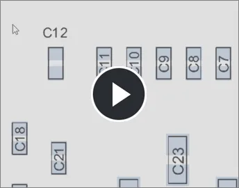
When multiple designators on a Board Assembly View are overlapped, use the View » Select Overlapped command (shortcut: Shift+Tab) to select overlapping designators. When you select the topmost overlapped designator, the next will be selected. Use the command again to select the next, and so on.
Displayed layer data
Further PCB topology information is included in a Board Assembly View by enabling layer data associated with the current view (Top or Bottom) in the Properties panel.
With a Top side assembly view for example, the panel’s Topology option (under Show additional data) displays the board Top Layer – and enables SMD/through-hole pad options, which may be selected independently. The Mask and Paste options overlay the Top solder mask and paste layers, as determined by the current view side (Top, in this case).
Additionally, the Properties panel’s Layers tab is populated with the mechanical layers available in the board design. Multiple layers can be selected for display, where their draw order determined by the listed order. Use the  and
and  buttons to specify a layer’s relative list/draw order.
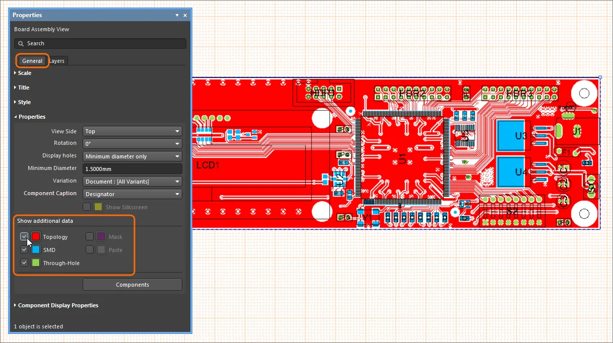
To change the color of a layer overlay on a view, select its associated color icon to open the color selector drop-down, which offers standard color shades plus definable RGB levels. The transparency level of a layer color, such as might be used for the solder Mask overlay, is available in the Define Custom Color part of the selector as a percentage slider.

Board Assembly View Properties
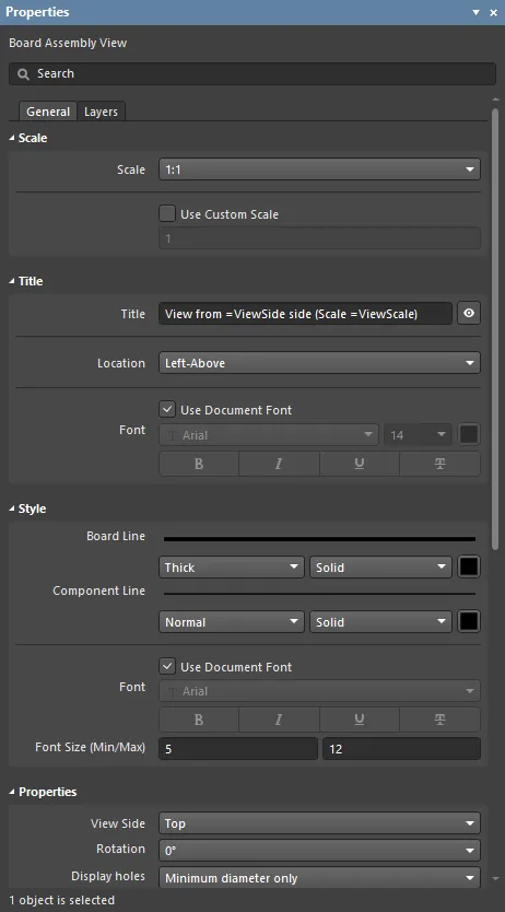
The Board Assembly View mode of the Properties panel (when a component is selected in the Assembly View).
General tab
Scale
- Scale – select the drop-down to choose from a range of preset scale ratios to set the visible size of the object. This option is not available if the Use Custom Scale option is checked.
- Use Custom Scale – select this option to enter a specific scale in its associated field. The scaling of the drawing object is relative to
1, where 0.9 would represent a scale of 90%.
Title
- Title – the title name string that will be displayed (if enabled) with the Assembly View object. Use the associated
 button to toggle its visibility. Enter the title name and any desired system/custom parameters to create a meaningful name for the placed view. See the Parameters tab in the Properties panel Document Options mode for a list of the currently available parameters.
- Location – select the drop-down to choose from a range of relative locations for the title. The Manual option is automatically selected if the title is manually moved (dragged and dropped to a new location).
- Font – sets the displayed font used for the view's title string.
- Use Document Font checkbox selected – the title font used is that defined by the document options. See the Document Font entry in General section of the Properties panel when in Document Options mode.
- Use Document Font not selected – use the drop-down menus to choose the desired font type and size and select the lower buttons to enable text attributes. The associated color button (
 ) opens the color selector where the font color can be specified by RGB or HEX value, by freeform selection, or from a range of presets. Note that the slider control sets the color Opacity level, where 0% represents full transparency.
Style
- Board Line – the thickness and style of the Assembly View's border/outline. Use the line weight drop-down menu to choose from a range of line thickness presets and the line pattern menu to choose from a range of line styles. The associated color button (
 ) opens the line color selector where the font color can be specified by RGB or HEX value, by freeform selection, or from a range of presets. Note that the slider control sets the color Opacity level, where 0% represents full transparency.
- Component Line – the line thickness and style used to render the component geometry in the Assembly View. Use the line weight drop-down menu to choose from a range of line thickness presets and the line pattern menu to choose from a range of line styles. The associated color button (
 ) opens the line color selector where the font color can be specified by RGB or HEX value, by freeform selection, or from a range of presets. Note that the slider control sets the color Opacity level, where 0% represents full transparency.
- Font – the font style used to notate the view's board components (designator, BOM entry etc.). Use the drop-down menu to choose the desired font type and select the lower buttons enable text attributes.
- Use Document Font checkbox selected – the title font used is that defined by the document options. See the Document Font entry in General section of the Properties panel when in Document Options mode.
- Use Document Font not selected – use the drop-down menus to choose the desired font type and size and select the lower buttons to enable text attributes. The associated color button (
 ) opens the color selector where the font color can be specified by RGB or HEX value, by freeform selection, or from a range of presets. Note that the slider control sets the color Opacity level, where 0% represents full transparency.
- Font Size (Min/Max) – the minimum and maximum font size that can be automatically applied to a component when its Component Designator property (see below) is set to Center/Fit, where designators are auto-scaled to fit into the component outline.
Properties
-
View Side – the direction of view used to render the board drawing. Use the drop-down menu to select from a range of preset view directions.
When the Left (True Geometry), Right (True Geometry), Front (True Geometry) or Back (True Geometry) option is selected, the view of the whole board with all components is calculated at once, so these options can result in a more precise view in some cases, while the calculation time might increase. For a side view, it is recommended to use one of these options if their performance is sufficient. Otherwise, use the Left, Right, Front or Back option.
- Rotation – the angle of rotation used to render the board drawing, as applied by the drop-down menu.
- Display holes – use the drop-menu to set which board (through) holes will be shown.
- Minimum Diameter – sets the smallest board hole size that is shown when the
Minimum diameter only option is selected for Display Holes.
- Variation – select a project PCB Variant (if available) as the data source for the Assembly View. The
Document:xx option is a Variant specified for the document under Document Options in the Properties panel (Source section).
In the placed Assembly View, omitted variant components are not shown or are indicated as a colored mesh as determined by the Variants Display and Pattern settings (under General) in the Properties panel's Document Options mode. See Design Variants for an overview of managing board design variations.
- Component Caption – set the parameter source for the text captions associated with components (
Designator or BOM Item Position) from the drop-down menu.
- Show Silkscreen – use the drop-down to select from the following:
- None - select to not show the silkscreen.
- With Components - select to show the appropriate silkscreen overlay with components on the drawing (Top or Bottom overlay, depending on View Side setting).
- Without Components - select to show the appropriate silkscreen overlay without components on the drawing (Top or Bottom overlay, depending on View Side setting).
- Use the color selection button to specify the graphic overlay color.
Show additional data
- Topology – check to enable an overlay of the board layer associated with the current View Side (Top or Bottom), rendered in the color set by the associated button (
 ). This option also checks the SMD/Through-Hole pad options, which may be enabled independently.
A board that has multiple
Layer Stack regions, such as a
Rigid-Flex design, is likely to have a different Topology (outer layers) in each region. Draftsman allows for this by displaying the appropriate outer layer for each region – say, the
Top Layer for the Rigid region and
Mid-Layer 2 for the Flex region.
- SMD and Through-Hole – check these options for their respective pads shapes to be rendered in the Assembly View. Select their associated color buttons to specify the pad display color.
- Mask and Paste checkboxes – check these options enable the overlay of the board solder Mask/Paste layers associated with the current View Side (Top or Bottom), rendered in the color and transparency set via their associated color buttons.
- Components – click to open the Component Display Properties dialog where the display configuration for all components is available.
Component Display Properties
The settings in this section affect all components on the Assembly View unless a specific component is selected in the design space, where the settings will apply to the selected component. The available property fields are equivalent to those available in the Component Display Properties dialog (when its Show option is set to Components).
- Component – identifies the currently selected component (
Designator and Name), or indicates All components when the overall Assembly View is selected.
- Component Body – enable the check box to display component bodies in the Assembly View, and use the drop-down menu to select the data source used for rendering the component graphic. The range of options match those available under the Geometry tab of the Component Display Properties dialog. The associated
 button is used to specify the component outline color through the color selector pop-up window.
- Designator - sets the Designator parameter position relative to the component graphic. Use the drop-down menu to choose from a range of positions (which match those available in the Component Display Properties dialog). Toggle the checkbox to enable/disable the designator's visibility. The Manual option is automatically selected if the component's Designator is manually moved (dragged and dropped to a new location).
- Comment - enable the check box to display comments in the Assembly View and use the drop-down menu to select the data source used for rendering the comment.
- Reference Marker – enable the component reference marker graphic by selecting
Inside contour from the drop-down menu. The Reference Marker can also be specified in the Component Display Properties dialog.
- Hatching Pattern – displays and sets the component graphic fill pattern and color, which is used to render the component's profile when displayed in a board Section View. Select the associated
 button to access the fill options.
Pattern – the graphic pattern for the component profile fill. Select Solid fill or an ANSI pattern from the drop-down menu, and use the associated color buttons ( ) to specify colors for the fill and/or hatch pattern. Select a no-fill preset or an opacity level of
 0% to set the color as transparent.Scale – the relative line spacing of the applied ANSI hatch pattern.Rotation – the angle of the ANSI hatching lines, where a value of 0 is equivalent to 45°.Hatch Thickness – the line weight of the ANSI pattern lines.
- Designator Font Size – set the font size used for the selected component's designator. This field becomes available when the Use Document Font option in the panel's Style section is unchecked – note the font size is automatically scaled if the component designator positioning is set to
Center/Fit (the default).
- Apply changes to all instances of same BOM item – check this option to apply a change in the designator Location and Font size to all board components of the same type (those that share the same BOM entry). This is equivalent to locating and changing the properties of that component's BOM entry in the Component Display Properties dialog.
► ![]() Apply to all instances example
Apply to all instances example
Layers tab
The panel's Layers tab provides a tabular listing of the mechanical layers available in the board design, along with their visibility and color settings.
- Layer visibility – enable a layer's visibility setting (
 ) to allow its content to be rendered as an overlay on the selected Assembly View.
- Layer color – select a layer's
 button to change its overlay color on the Assembly View using the
 ![]() color selector drop down, which offers standard color shades plus definable RGB levels.
color selector drop down, which offers standard color shades plus definable RGB levels.
- Move Up/Down buttons – use the buttons to change the listed position of the selected layer and therefore its draw order relative to other layers. The topmost enabled layer in the list is rendered last, on top of the next enabled layer that is lower in the list, and so on – the list order represents the draw order.
Layers enabled in the Layers tab have a higher draw priority than those enabled in the panel's Show additional data section under the General tab.