The Inspector button opens the Inspector panel, which provides universal editing access to the properties of documents and objects in design editors. The panel dynamically determines its content based on the document or object that is currently selected and presents specific properties and settings that relate to that document/object.
The Inspector panel can be accessed in the following ways:
-
From the schematic and schematic library editors by choosing View | Schematic | Inspector from the ribbons.

-
From the PCB and PCB library editors by choosing View | PCB | Inspector from the ribbons.

-
From the Layer Stack Manager by choosing Home | Settings | Inspector from the ribbons.

- By double-clicking on an object in the design space.
- Using the F11 keyboard shortcut.
Schematic Support
When the active document is a schematic document (*.SchDoc) and no design object is selected in the design space, the Inspector panel presents the Document Options. The following section contains information about the options and controls available.
Document Options
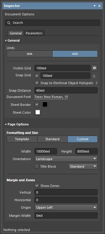
General Tab
General
- Units - select the desired unit. Choose either mm or mils.
- Visible Grid - enter the desired grid. Toggle the eye icon to show/hide the grid in the design space.
- Snap Grid - check the box to enable snap grids. Enter the desired grid in the text box or use the G shortcut to cycle through the different grids.
- Snap to Electrical Object Hotspots - enable to use the snap grid to snap to an object's electrical hotspots or use the Shift+E shortcut.
- Snap Distance - when the cursor is within this distance from an enabled object snap point (and snapping is enabled for the active layer), the cursor will snap to that point.
- Document Font - set the font size, style and any additional font attributes that will be used for the text associated with all objects in the document sheet. For any given object, the font settings may be overridden in its corresponding Inspector panel mode, which is enabled when that object is selected.
- Sheet Border - check the box to enable a sheet border then click the colored box to change the border color.
- Sheet Color - click the colored box to change the sheet color.
Page Options
- Formatting and Size
- Template mode – set the page size and format by selecting from a range of predefined schematic sheet templates. The list includes templates found on the Data Management - Templates page of the System Preferences.
- Standard mode – set the sheet size to a standard page format.
- Sheet Size – use the drop-down menu to select from a list of standard page dimensions.
- Width/Height – the dimensions of the current page size in the current document units.
- Orientation - use the drop-down to select the desired orientation.
- Title Block - enable this option to display one of two predefined title blocks on the schematic sheet. Use the associated drop-down to choose from either a
Standard or ANSI title block style.
- Custom mode – set the sheet size to specified custom dimensions.
- Width – enter the required sheet width measurement.
- Height – enter the required sheet height measurement.
- Orientation - use the drop-down to select the desired orientation.
- Title Block - enable this option to display one of two predefined title blocks on the schematic sheet. Use the associated drop-down field to choose from either a
Standard or ANSI title block style.
- Margin and Zones - defines the size of the sheet border graphics and its zone divisions. Uncheck the Show Zones box to hide the zone divisions in the border graphics.
- Vertical – set the number of divisions (rows) in the vertical sheet margin. The alpha-numeric zone labeling type is defined by the Origin setting.
- Horizontal – set the number of divisions (columns) in the horizontal sheet margin.
- Origin – sets which corner of the document sheet(s) the perimeter zone alpha-numeric indicators will begin from (zone position
A-1 or 1-A).
- Margin Width – set the distance (in the current units) between the page edge and each of the four border lines as indicated by the arrows associated with each entry field.
Parameters Tab
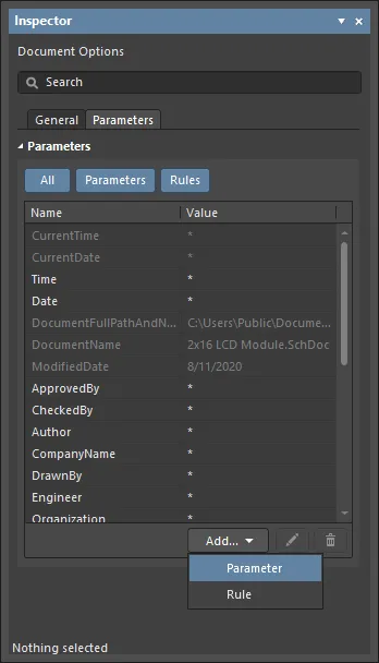
The Inspector panel Parameters tab lists all available Parameters and Rules available in the current project document.
- All - select to view both Parameters and Rules.
- Parameters - select to only view Parameters.
- Rules - select to only view Rules.
- Parameters
- Name and Value columns – lists the available parameters grouped by type.
- Rules
- Name and Value columns – lists the current specified rules and their values.
- Add - use the drop-down menu to select to add a Parameter or a Rule. Selecting to add a new Rule will open the Choose Design Rule Type dialog to specify the type of rule to be used when adding a parameter as a rule to a supported design object in the schematic domain or a schematic document.
-
 - only accessible when a rule is selected. Click to open the Edit PCB Rule dialog to edit the selected rule.
-
 - click to delete the currently selected parameter or rule.
When a design object is selected, the panel will present options specific to that object type. The following table lists the object types available for placement on a schematic sheet. Click a link to access the information for that object.
Modifying Data Strings
Using Formulas
The Inspector panel has the ability to modify data strings using formulas in the schematic editor. Formulas and expressions offer a convenient method of modifying attribute parameters of multiple selected objects to change their location or string-based values. This allows you to apply a specific expression to the selected string objects. The expression can include any built-in arithmetic operators and functions that apply to strings (found in Pascal). If you want to use the current value for the attribute as part of the expression, you will need to make reference to this original value either by using the full name of the attribute or by using the exclamation character (the supported substitute for the name of the attribute currently being modified). When using attribute names, if any names contain spaces, these must be replaced by the underscore character.
Using the Smart Edit Feature
Some parameter string fields also provide access to the Smart Edit dialog when multiple objects are selected, which is opened with the associated  button.
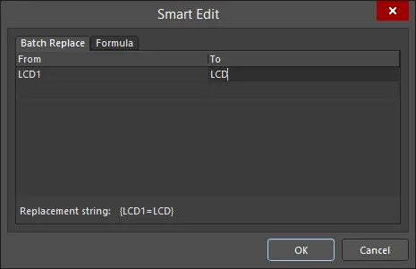
The dialog offers two methods for performing string modification accessed from the Batch Replace and Formula tabs.
Schematic Library Support
When the active document is a schematic library document and no objects are selected in the design space, choose Tools | Document Options to open the Inspector panel in the Library Options mode. The following collapsible section contains information about the options and controls available.
Library Options

Selection Filter
The options in this section of the panel determine which schematic library objects may be selected in the design space.
- All Objects button – select remove object filtering so that all types of objects may be selected.
- Object buttons – toggle each object button to enable/disable the ability to select that object type.
General
- Units - select the desired unit. Choose either mm or mils.
- Visible Grid - enter the desired grid. Toggle the eye icon to show/hide the grid in the design space.
- Snap Grid - check the box to enable snap grids. Enter the desired grid in the text box or use the G shortcut key.
- Sheet Border - check the box to enable a sheet border then click the colored box to change the border color.
- Sheet Color - click the colored box to change the sheet color.
- Show Hidden Pins - enable to show hidden pins on the design space.
- Show Comment/Designator - enable to show comments/designators on the design space.
When a design object is selected, the panel will present options specific to that object type. The following table lists the object types available for placement within the library design space. Click a link to access the information for that object.
PCB Support
When the active document is a PCB document (*.CMPcbDoc) and when no design object is currently selected in the design space, the Inspector panel presents the Board mode. The following collapsible sections contain information about the options and controls available:
Board
Snap Options
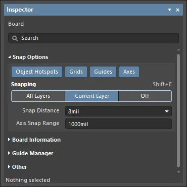
- Object Hotspots - use to toggle whether the cursor will snap to the object's hotspot.
- Grids - used to toggle whether the cursor will snap to the active design space grid. When this option is enabled the cursor will pull, or snap, to the nearest snap grid location. The active snap grid is displayed on the Status bar.
- Guides - used to toggle whether the cursor will snap to manually placed linear or point Snap Guides. A Snap Guide will override the Snap Grid.
- Axes - used to toggle whether the cursor will axially-align (in either the X or Y direction) to the enabled Objects for snapping. The Axis Snap Range defines the distance within which X or Y axial-alignment will occur. A dynamic alignment guideline is displayed when alignment is achieved, from the current cursor location to the axially-aligned object snap point (hotspot).
- Snapping - select directly or use the Shift+E shortcut to select whether you want to snap to objects on:
- All Layers - enable this option to allow the cursor to snap to any electrical object on any visible layer.
Current Layer - enable this option to allow the cursor to only recognize and snap to objects placed on the currently selected layer.- Off - enable this option to turn off snapping to hotspots.
- Snap Distance - when the cursor is within this distance from an enabled object snap point (and snapping is enabled for the active layer), the cursor will snap to that point.
- Axis Snap Range - when the cursor is axially-aligned and within this distance from an enabled object snap point (and the Axes feature is enabled), a dynamic guideline will display to indicate that alignment has been achieved.
Board Information

- Board Size
- Horizontal/Vertical: the overall length of the board in the horizontal (X) and vertical (Y) directions.
- Components/Layers/Nets/Primitives & Others - displays information for each listed category such as the total number of the listed item.
- Reports - click to open the Board Report dialog in which you can specify the content to be included when generating a detailed report for the board.
Guide Manager
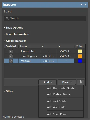
- Guide Manager - where a range of manual Snap Guides and Snap Points for the board can be defined and managed.
- Add - click to add a new snap guide or snap point. Choose the corresponding command for the required guide type from the associated menu; an entry for the new guide/point will be added to the grid. The following guide types are available:
Add Horizontal Guide - use this command to add a horizontal guideline at the desired Y-coordinate location in the design space.Add Vertical Guide - use this command to add a vertical guideline at the desired X-coordinate location in the design space.Add +45 Guide - use this command to add a 45 degree (y=x) guideline that passes through the desired X,Y coordinate location in the design space.Add -45 Guide - use this command to add a -45 degree (y=-x) guideline that passes through the desired X,Y coordinate location in the design space.Add Snap Point - use this command to add a point snap guide. This is a hotspot that you manually mark within the confines of the default snap grid. During an interactive process such as placing or moving an object, that objects' hotspot will 'snap' to a point snap guide when it passes into close proximity with it.
- Place - click to place a guide. Select the guide type from the drop-down:
Place Horizontal Guide - use this command to place a horizontal guideline at the desired Y-coordinate location in the design space.Place Vertical Guide - use this command to place a vertical guideline at the desired X-coordinate location in the design space. Place +45 Guide - use this command to place a 45 degree (y=x) guideline that passes through the desired X,Y coordinate location in the design space.Place -45 Guide - use this command to place a -45 degree (y=-x) guideline that passes through the desired X,Y coordinate location in the design space.Place Snap Point - use this command to place a point snap guide. This is a hotspot that you manually mark within the confines of the default snap grid. During an interactive process such as placing or moving an object, that objects' hotspot will 'snap' to a point snap guide when it passes into close proximity with it.
-
 - click to delete the currently selected guide.
Other
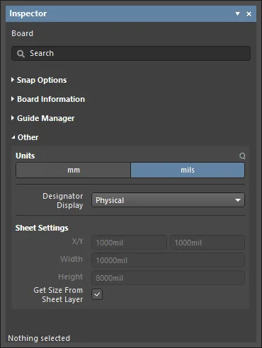
- Units - use to select the default measurement units for the current PCB document. Default units are used to display any distance-related information on the screen or in reports. The default units are always used if a unit's suffix (mm or mil) is not entered when specifying any distance related information.
- Designator Display - use this field to determine how designators are to be displayed. It can be difficult to position the designator strings in a multi-channel design, as they can end up being quite long. As well as choosing a naming option that results in a short name, another option is to display just the original, logical component designation instead. For example,
C30_CIN1 would display as C30. This would of course necessitate some other notation being added to the board to indicate the separate channels, such as a box being drawn around each channel on the component overlay. The following options are available:
Physical - choose to display the physical designators. These are the designators displayed on the compiled tab views of the schematic source documents. For multi-channel designs, the designator format is determined by the Designator Format field on the Multi-Channel tab of the Project Options dialog. Physical designators are unique, e.g., R1_CH1.Logical - choose to display the logical designators. These are the designators displayed on the Editor tab views of the schematic source documents. Logical designators are not unique; for example, the R1_CH1 physical designator will become simply R1.
- Sheet Settings - use this region to configure the PCB sheet.
- X/Y - enter the X and Y coordinates for the bottom left corner of the sheet. This distance is measured from the absolute origin, which is the bottom left corner of the design space. The distance can be defined in either metric or imperial units regardless of the default units (which are determined by the Units setting). To specify the units when entering a size, add the mm or mil suffix to the value.
- Width - enter a width for the sheet here. The sheet provides an area that emulates the traditional drawing sheet and is useful for placing information such as dimensions, notes and title blocks. Information placed on mechanical layers can be linked to the sheet so that they only display when the sheet is being displayed. Sheet size can be defined in either metric or imperial units regardless of the default units (which are determined by the Units setting). To specify the units when entering a size, add the mm or mil suffix to the value.
- Height - enter a height for the sheet here. The sheet provides an area that emulates the traditional drawing sheet and is useful for placing information such as dimensions, notes and title blocks. Information placed on mechanical layers can be linked to the sheet so that they only display when the sheet is being displayed. Sheet size can be defined in either metric or imperial units regardless of the default units (which are determined by the Units setting). To specify the units when entering a size, add the mm or mil suffix to the value.
- Get Size From Sheet Layer - enable this option to size the sheet from the sheet layer.
When a design object is selected, the panel will present options specific to that object type. The following table lists the object types available for placement within a PCB document. Click a link to access the information for that object.
Although
Tracks and
Lines are actually the same objects, the difference is how the software behaves during their placement, which is why there are different commands.
After launching the Home | Place | Line command, the cursor will change to a cross-hair and the editor will enter line placement mode. Placement is made by performing the following actions:
- Click to define the starting position of the line.
- Move the cursor to set the length and angle the line then click again to complete placement.
- Continue placing further lines or right-click or press Esc to exit the placement mode.
PCB Library Support
When the active document is a PCB Library document and no design object is currently selected in the design space, the Inspector panel presents the Library Options. The following collapsible section contains information about the options and controls available.
Library Options

Snap Options
- Object Hotspots - use to toggle whether the cursor will snap to an object's hotpots.
- Grids - use to toggle whether the cursor will snap to the active design space grid. When this option is enabled the cursor will pull, or snap, to the nearest snap grid location. The active snap grid is displayed on the Status bar.
- Guides - used to toggle whether the cursor will snap to manually placed linear or point Snap Guides. A Snap Guide will override the Snap Grid.
- Axes - used to toggle whether the cursor will axially-align (in either the X or Y direction) to the enabled Objects for snapping. The Axis Snap Range defines the distance within which X or Y axial-alignment will occur. A dynamic alignment guide line is displayed when alignment is achieved from the current cursor location to the axially-aligned object snap point (hotspot).
- Snapping - select directly or use the Shift+E shortcut to select whether you want to snap to objects on:
- All Layers - enable this option to allow the cursor to snap to any electrical object on any visible layer.
Current Layer - enable this option to allow the cursor to only recognize and snap to objects placed on the currently selected layer.- Off - enable this option to turn off snapping to hotspots.
- Snap Distance - when the cursor is within this distance from an enabled object snap point (and snapping is enabled for the active layer), the cursor will snap to that point.
- Axis Snap Range - when the cursor is axially-aligned and within this distance from an enabled object snap point (and the Axes button is enabled), a dynamic guideline will display to indicate that alignment has been achieved.
Guide Manager
Other
- Units - use to select the default measurement units for the current PCB Library document. Default units are used to display any distance related information on the screen or in reports. The default units are always used if a unit's suffix (mm or mil) is not entered when specifying any distance related information.
- Route Tool Path - use the drop-down to choose the mechanical layer (from all those currently enabled for use in the design) on which to define the route tool path for the board.
When a design object is selected, the panel will present options specific to that object type. The following table lists the object types available for placement within the PCB library design space. Click a link to access the information for that object.
Interactive Routing Support
When the active document is a PCB document (*.CMPcbDoc) and you are currently using the interactive routing tool, the Inspector panel presents options pertinent to that tool. The following section contains information about the options and controls available.
Interactive Routing
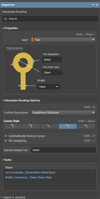
- Properties - use the options to configure the interactive routing.
- Routing Mode - use the drop-down or use the Shift+R shortcut to cycle through the desired routing modes. The following choices are available:
Ignore Obstacles - select to ignore existing objects (routing can be freely placed). Violations are highlighted. Push Obstacles - select to have the Interactive Router move existing tracks out of the way. This mode can also push vias to make way for the new routing. If this mode cannot push an obstacle without causing a violation, an indicator appears to show that the route is blocked.HugNPush Obstacles - select to have the Interactive Router hug existing tracks, pads, and vias as closely as possible and where necessary, push obstacles to continue the route. If this mode cannot hug or push an obstacle without causing a violation, an indicator appears to show that the route is blocked.Stop At First Obstacle - in this mode, the routing engine will stop at the first obstacle that gets in the way.
- Corner Style - select the desired routing corner style or use the Shift+Spacebar shortcut to cycle through the corner styles.
- Automatically Remove Loops - enable to automatically remove any redundant loops that are created during manual routing. This allows you to re-route a connection without having to manually remove redundant tracks. However, there are times when you need to route nets such as power nets and you need loops. You can toggle this option for a selected net by using the Shift+D shortcut to override this global setting for the same net.
- Pin Swapping - check this option to enable pin swapping or use the Shift+C shortcut.
-
Subnet Jumper Length - specify the desired Subnet Jumper length.
Jumpers, which are also referred to as wire links, allow you to replace routing with a Jumper component.
- The Rules region lists the constraints defined by the applicable design rules. Click a constraint to open the respective Edit PCB Rule dialog to define the rules.
Interactive Differential Pair Routing Support
When the active document is a PCB document (*.CMPcbDoc) and you are currently using the interactive differential pair routing tool, the Inspector panel presents options pertinent to that tool. The following collapsible section contains information about the options and controls available.
Interactive Differential Pair Routing
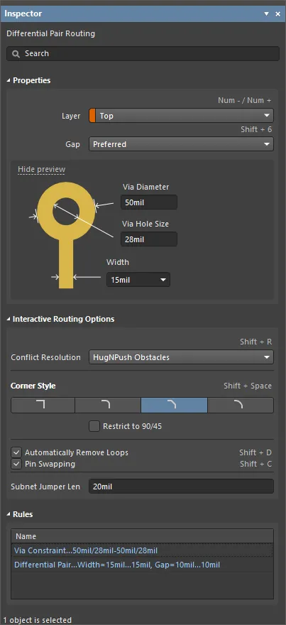
- Properties - use the options to configure the routing.
- Routing Mode - use the drop-down or use the Shift+R shortcut to cycle through the desired routing modes. The following choices are available:
Ignore Obstacles - select to ignore existing objects (routing can be freely placed). Violations are highlighted. Push Obstacles - select to have the Interactive Router move existing tracks out of the way. This mode can also push vias to make way for the new routing. If this mode cannot push an obstacle without causing a violation, an indicator appears to show that the route is blocked.HugNPush Obstacles - select to have the Interactive Router hug existing tracks, pads, and vias as closely as possible and where necessary, push obstacles to continue the route. If this mode cannot hug or push an obstacle without causing a violation, an indicator appears to show that the route is blocked.Stop At First Obstacle - in this mode, the routing engine will stop at the first obstacle that gets in the way.
- Corner Style - select the desired routing corner style or use the Shift+Spacebar shortcut to cycle through the corner styles.
- Restrict to 90/45 - enable to restrict the routing to 90 degrees and 45 degrees only.
- Automatically Remove Loops - enable to automatically remove any redundant loops that are created during manual routing. This allows you to re-route a connection without having to manually remove redundant tracks. However, there are times when you need to route nets, such as power nets and when you need loops; you can toggle this option for a selected net by using the Shift+D shortcut to override this global setting for the same net.
- Pin Swapping - check this option to enable pin swapping or use the Shift+C shortcut.
-
Subnet Jumper Length - specify the desired Subnet Jumper length.
Jumpers, which are also referred to as wire links, allow you to replace routing with a Jumper component.
- The Rules region lists the constraints defined by the applicable design rules. Click a constraint to open the respective Edit PCB Rule dialog to define the rules.
Interactive Multi-Routing Support
When the active document is a PCB document (*.CMPcbDoc) and you are currently using the interactive multi-routing tool, the Inspector panel presents options pertinent to that tool. The following collapsible section contains information about the options and controls available.
Interactive Multi-Routing

- Layer - use the drop-down to specify on which layer the routing is located.
- Via Hole Size - specify the via hole size or use the 4 shortcut key during routing.
- Via Diameter - specify the via hole diameter.
- Width - use the slider bar to specify the width. Farther to the left (Min) signifies that the design rule minimum width defined for the current net will be used. Preferred signifies that the design rule preferred width defined for the current net will be used. Farther to the right (Max) signifies that the design rule maximum width defined for the current net will be used.
- Pickup From Existing Routes - enable to use the existing track width when routing from a placed track. That is, even if the current routing width is different from the existing track, the existing track width will be adopted when you continue the route from it.
- Bus Spacing - enter the desired bus routing or use the Shift+B shortcut.
- From Rule - click to assign bus spacing based on the existing design rule.
- Routing Mode - use the drop-down or use the Shift+R shortcut to cycle through the desired routing modes. The following choices are available:
Ignore Obstacles - select to ignore existing objects (routing can be freely placed). Violations are highlighted. Push Obstacles - select to have the Interactive Router move existing tracks out of the way. This mode can also push vias to make way for the new routing. If this mode cannot push an obstacle without causing a violation, an indicator appears to show that the route is blocked.HugNPush Obstacles - select to have the Interactive Router hug existing tracks, pads, and vias as closely as possible and, where necessary, push obstacles to continue the route. If this mode cannot hug or push an obstacle without causing a violation, an indicator appears to show that the route is blocked.Stop At First Obstacle - in this mode, the routing engine will stop at the first obstacle that gets in the way.
- Corner Style - select the desired routing corner style or use the Shift+Spacebar shortcut to cycle through the corner styles.
- Restrict to 90/45 - enable to restrict the routing to 90 degrees and 45 degrees only.
- Automatically Remove Loops - enable to automatically remove any redundant loops that are created during manual routing. This allows you to re-route a connection without having to manually remove redundant tracks. However, there are times when you need to route nets such as power nets and you need loops - you can toggle this option for a selected net by using the Shift+D shortcut to override this global setting for the same net.
- The Rules region lists the constraints defined by the applicable design rules. Click a constraint to open the respective Edit PCB Rule dialog to define the rules.
Layer Stack Support
When the active document is a Layer Stack document (*.CMPcbDoc [Stackup]), the Inspector panel presents options pertinent to that layer stack depending on the chosen tab (located at the bottom of the Layer Stack). Tabs include Stackup and Via Types. The following collapsible sections contain information about the options and controls available for the various tabs.
Stackup Tab
The Stackup tab allows you to edit the layer properties of the Layer Stack.
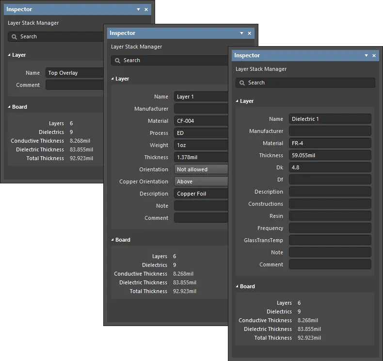
The Layer Stack Manager mode of the Inspector panel: an Overlay layer (left image), a signal layer (middle image), and a dielectric layer (right image).
- Layer
- Name - the name of the layer.
- Manufacturer - the layer manufacturer.
- Material - the layer material.
- Thickness - the thickness of the signal layer.
- Dk - this is the Dielectric Constant (also referred to as εr in electromagnetics). This indicates the relative permittivity of an insulator material, which refers to its ability to store electrical energy in an electric field. For insulating purposes, a material with a lower dielectric constant is better and in RF applications, a higher dielectric constant may be desirable. In addition, the lower the relative dielectric constant, the closer the performance of the material to that of air. This property is critical to matching the impedance requirements of certain transmission lines.
- Df - this is the Dissipation Factor. This indicates the efficiency of insulating material by showing the rate of energy loss for a certain mode of oscillation, such as mechanical, electrical, or electromechanical oscillation. In other words, this is the property of a material that describes how much of the energy transmitted is absorbed by the material. The greater the loss tangent, the larger the energy absorption into the material. This property directly impacts the signal attenuation at high speeds.
- Process - displays the copper plating process that is applied to the base copper that makes up the outer signal layers of the PCB (the Top Layer and Bottom Layer).
- Weight - the weight of the copper per unit area, usually expressed in ounces/square foot (e.g., 0.5 oz/ft2).
- Orientation - this defines which way the components point (orient) on that layer. For the top and bottom sides, this is set automatically for a new board. Choices include: Not allowed, Top, and Bottom.
-
Copper Orientation - this defines the direction that the copper is laminated onto the core. Use the drop-down to select Above or Below, which determines the direction from which it is etched.
The Copper Orientation can also be chosen using the drop-down in the Copper Orientation column of the Layer Stack. To enable the column, right-click in the header, choose Select columns then enable the Copper Orientation entry in the Select columns dialog.
- Frequency - this is the frequency at which the material is tested and the value that Dk / Df corresponds to a certain frequency. Frequency is also taken from material references.
- Description - enter a meaningful description.
- Constructions - for dielectric layers, this displays the constructions of the layer. The numerical reference relates to the structure of the woven glass fabric used in the dielectric layer material; these are standard references used by PCB fabricators.
-
Resin - displays the resin percentage of the layer.
Notes on Constructions and Resin:
The choice of laminate construction can significantly impact both cost and performance. As should be expected, a single-ply construction will typically represent cost savings compared to a multiple-ply construction. The magnitude of these savings will depend on the specific glass styles involved and a host of other parameters. Performance can also be affected and should be considered when specifying the constructions to be used. First, single-ply constructions are often lower in resin content. The other main benefit of single-ply constructions is dielectric thickness control, beyond resin content considerations. Tighter thickness tolerances can be achieved using a single-ply construction.
Constructions with relatively lower resin contents are often preferred since they result in less z-axis expansion and can, therefore, improve reliability in many applications. In addition, lower resin contents can also improve dimensional stability, resistance to warpage, and dielectric thickness control. On the other hand, constructions with higher resin contents result in lower dielectric constant values, which are sometimes preferred for electrical performance. In addition, a certain minimum resin content is required to ensure adequate resin-to-glass wet-out and to prevent voids from occurring within the laminate. The ability to wet out the glass filaments fully with resin is also important for CAP resistance.
- GlassTransTemp - this is the Glass Transition Temperature (also known as TG) and is the temperature at which the resin changes from a glass-like state to an amorphous state changing its mechanical behavior, i.e. expansion rate.
- Note - enter any pertinent notes for the layer.
- Comment - enter any necessary comments for the layer.
- Board
- Layers - the number of conductive layers.
- Dielectrics - the number of dielectrics.
- Conductive Thickness - this is the sum of the thicknesses of all signal and plane layers (all copper or conductive layers).
- Dielectric Thickness - the thickness of dielectric layer(s).
- Total Thickness - the total thickness of the finished board.
Via Types Tab
The Via Types tab is used to define the allowed Z-plane layer-spanning requirements of the via(s) used in the design.

- Via Type
- Name - the name of the via. The software automatically detects the type based on the layers that have been chosen and names the via accordingly.
- First layer - the first layer the via spans.
- Last layer - the last layer the via spans.
- Mirror - when enabled, a mirror of the current via that spans the symmetrical layers in the layer stack is created.
- Board
- Layers - the number of conductive layers.
- Dielectrics - the number of dielectrics.
- Conductive Thickness - this is the sum of the thicknesses of all signal and plane layers (all copper or conductive layers).
- Dielectric Thickness - the thickness of dielectric layer(s).
- Total Thickness - the total thickness of the finished board.