
One of the most time-consuming phases of board design is routing the nets. While the rules system handles the design constraints, such as the widths, via sizes, clearances, and so on, it is down to the designer to place the many thousands of track segments required to fully route a board.
Autorouters can ease this pain but are generally regarded as inadequate because:
-
They fail to correctly consider the myriad of subtle design constraints that a human designer instinctively applies as they route.
-
They take so long to fully configure that it is often more efficient to simply get on with routing the board interactively.
-
The cleanup can be such a long and difficult process that it is often more efficient to route the board interactively.
The holy grail of PCB routing is to quickly produce high-quality results, that meet the design rules, under the control of the designer. This is the challenge that ActiveRoute sets out to achieve.
Improving the Completed Routes
Complementing, but separate to ActiveRoute are the Glossing and Retrace features. These can be used to improve the quality of any existing routing, regardless of how it was created.
Glossing defaults to on and will run when ActiveRoute completes - this can be disabled in the PCB ActiveRoute panel if required. Glossing also has its own set of options, including the ability to curve the routing corners.
► Learn more about Glossing & Retracing of Existing Routes
What is ActiveRoute?
ActiveRoute is an automated interactive routing technology that delivers efficient multi-net routing algorithms, which is applied to the specific nets or connections you select. ActiveRoute also allows the designer to interactively define a route path or Guide, which then defines the river along which the new routes will flow.
The key ActiveRoute features that make this approach significantly better than a combination of regular interactive routing and auto-routing include:
-
Automatic optimization of the escape routes out of pin/via arrays - the most time-consuming aspect of manual routing.
-
High performance - signal nets routed < 1 second each.
-
Obeys design rules for width, clearance, layers, topology and rooms by net and net class, observing priorities.
-
Routes on multiple layers simultaneously and distributes the routes across those layers.
-
An intuitive Route Guide that the designer can use to direct the placement of routes.
-
Uses a River Route approach to give high completion rates without the need for vias.
-
Able to route through polygon planes and re-pour them (if the re-pour option is enabled).
-
Supports both single-ended and differential pair nets.
-
Finishes with a powerful glossing tool that further reduces the number of corners and shortens the routing.
What ActiveRoute is Not
ActiveRoute is not an autorouter. It is a guided interactive router that focuses on clean, high-quality routing of a set of selected nets. Use ActiveRoute in the same way as you would approach the interactive routing task: choose the nets of interest, enable the layers on which you would like those nets routed, think about the path they should follow, and route them.
If you select all of the nets on the board and ActiveRoute them, it is likely that you will be disappointed. ActiveRoute is not an autorouter; it cannot place vias and does not include power net routing strategies.
The PCB ActiveRoute Panel
ActiveRoute follows the criteria and restrictions defined by the PCB design rules, so using it is simply a matter of selecting the connections or nets of interest and running it. It does have a number of specific control features that are configured in the PCB ActiveRoute panel. The PCB ActiveRoute panel is used to configure and operate the various features provided by ActiveRoute, including: performing an interactive ActiveRoute; defining a Route Guide and the spacing of the routes within it; enabling automatic length tuning; and enabling automatic pin swapping. It is highly recommended that the PCB ActiveRoute panel be opened prior to starting ActiveRoute.
To open the PCB ActiveRoute panel, when a PCB is the active document:
To access ActiveRoute capabilities in Altium Designer, the ActiveRoute software extension must be installed. It can be installed or removed manually.
For more information about managing extensions, refer to the Extending Your Installation page (Altium Designer Develop, Altium Designer Agile, Altium Designer).
 Use the PCB ActiveRoute panel to control the ActiveRoute process.
The PCB ActiveRoute panel is used to:
-
Enable the signal layers on which ActiveRoute can route connections.
-
Perform an ActiveRoute on the selected connections.
-
Enable a post-ActiveRoute Glossing pass.
-
Define a Route Guide.
-
Configure the track-to-track spacing you would like to be used within the Route Guide.
-
Configure and enable length tuning of the routes placed by ActiveRoute.
-
Configure the Meander option, allowing ActiveRoute to define a longer routing path, which may help increase the completion rate.
-
Configure and enable pin swapping. ActiveRoute can pin swap during routing to help improve the routing quality.
ActiveRoute operates on the selected connections, some of the controls in the panel will only become active when there are connections selected.
The PCB ActiveRoute panel content is arranged in collapsible sections that are opened and closed using the ► icon associated with each section heading. The property control information included below is arranged by matching sections, and each collapsible section is opened/closed in the same manner.
Action

These are the primary options used to control ActiveRoute.
-
ActiveRoute - click the
 button in the panel to to perform an ActiveRoute on the selected connections. ActiveRoute attempts to route the selected connections, or if pads or vias are selected, all connections in those nets. Refer to the ActiveRoute page to learn more about Selection Techniques.
-
Route Guide - a route guide is a user-defined path that the selected connections are to be routed within by ActiveRoute. One of the primary objectives of ActiveRoute is to find the shortest overall set of route lengths, which may not be the desired path for every set of connections. The Route Guide provides the designer with a tool they can use to draft a specific path they would like the selected connections to flow along. The color of the Route Guide is determined by the layers made available for the ActiveRoute of the selected connections - if there is a single layer enabled it is drawn in that layer color, if there are multiple layers enabled it is drawn in the default Route Guide color.
-
To define a Route Guide, first select the connections that are to be routed within the guide, click the
 button in the panel, then click to define the guide start location, and continue to move the mouse and click to define the path. Once the path is defined, click the ActiveRoute button to route the selected connections along that path.
-
During Route Guide placement, the guide can be made wider or narrower by pressing the
 or
or  keys. The default width is the sum of the applicable width+clearance design rules for the selected connections, divided by the number of layers, multiplied by 1.3. Press the Backspace key to unwind the Guide if you need to define a different path.
-
ActiveRoute will attempt to space the routes in accordance with the design rules, it does not attempt to spread, or use all of the space available within a Route Guide. To spread the routes within a Route Guide, use the Track-Track Space in Route Guide feature, as described later on this page.
-
Tune Selected - when this option is enabled, the highest priority applicable Matched Length rule that is enabled in the Tune section of the panel, is applied.
-
Pin Swap Routing – pin swapping is supported in the PCB editor, enable this option to allow ActiveRoute to perform pin swapping during the routing process. As well as enabling this option, the required components must also be enabled in the Pin Swap section of the panel, as described below. To learn more about the pin swapping system, refer to the Pin, Pair and Part Swapping page.
-
Gloss Results – enable this option to automatically Gloss the ActiveRoute results. Glossing can also be applied to existing selected routes, to do this run the Route » Gloss Selected command (Ctrl+Alt+G). Refer to the Glossing & Retracing of Existing Routes page to learn more.
Layers
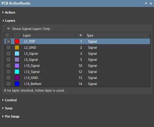
ActiveRoute can route on multiple layers simultaneously. While it cannot place vias to perform a layer change, it can distribute connections and nets across the available layers. The available layers are configured in the Layers section of the panel.
-
Show Signal Layers Only – by default, all available signal and plane layers are shown, enable this option to only display the signal layers.
-
List of Layers – enable the signal layers that ActiveRoute can route signals on. ActiveRoute will distribute the connections over the available signal layers. Note that ActiveRoute does not place vias to perform a layer change.
Control
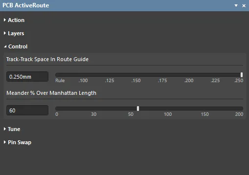
These controls are used to relax ActiveRoute's focus on spacing the tracks to meet the applicable clearance design rule, and to allow it to use a less direct route to complete a connection.
-
Track-Track Space in Route Guide – this control is used to instruct ActiveRoute how far apart to attempt to spread the connections being routed along the Route Guide (track center-to-track center). The setting must be made before the Route Guide is defined, so that the guide width can be correctly calculated to suit the spacing. Use the slider to select a value, or type a distance into the edit box.
-
Meander % Over Manhattan Length – ActiveRoute attempts to route the selected connections along the shortest possible path, or in other words, using the minimum amount of meandering. If the ActiveRoute completion rate is lower than expected, increasing the amount of allowed meander may help raise the completion rate. The default maximum Meander setting is 100%, meaning the routes are allowed to have a total route length of
Manhattan Length + 100% of Manhattan Length. Use the slider to select a value, or type a percentage into the edit box. Note that the meander setting is ignored when using the Route Guide, because the Route Guide is intended to be used to define a path which may significantly increase the meander.
Tune
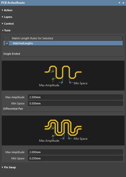
ActiveRoute can apply length tuning to connections currently being routed, or to selected existing routes.
-
Match Length Rules for Selected – all defined Matched Length design rules are listed here. Enable the rule to be used by ActiveRoute for the selected connections.
-
Single Ended – properties of the tuning accordion to be used to tune single ended signals.
-
Max Amplitude - maximum allowed amplitude of the tuning accordion. The amplitude is automatically decreased when there are obstacles, such as existing pads, vias or tracks, to ensure design rule clearances are maintained.
-
Min Space - the minimum edge-to-edge space between the zero-crossings of the accordion shape.
-
Differential Pair - properties of the tuning accordion to be used to tune differential pairs.
-
Max Amplitude - maximum allowed amplitude of the tuning accordion for the outer differential pair-member. The amplitude is automatically decreased when there are placement obstacles, to ensure design rule clearances are maintained.
-
Min Space - the minimum edge-to-edge space between the zero-crossings of the accordion shape for the inner differential pair-member.
Currently only the Mitered Lines tuning style is available with a corner miter of approximately 20%. The accordions placed by ActiveRoute are also not Unions. ActiveRoute length tuning support is under ongoing development, with other tuning styles and accordion Unions being evaluated.
Pin Swap

Functionally equivalent pins in a component can be configured to be swappable, select the Tools » Pin/Part Swapping » Configure command to do this. Before any pin swapping can be performed (interactively or by ActiveRoute), the project must be compiled (Project menu) each time it is opened.
-
Components with Pin Swap Enabled – all components that are enabled for pin swapping will be listed here, enable those you would like to be available for automatic swapping during an ActiveRoute.
Additional ActiveRoute Features
ActiveRoute is an automated interactive router and using it is simple and straightforward: select the connections then press Shift+A to ActiveRoute them in accordance with the design rules. ActiveRoute includes a number of other features and controls, giving the designer greater control over certain features and abilities.
These include:
-
Define the routing path and track spacing, by placing a Route Guide.
-
Allow a longer route path with the Meander control.
-
Automatically match the route lengths with length tuning.
-
Allow pin swapping to simplify the routing challenge.
Let's look at each of these in more detail.
Define the Path with the Route Guide
One of the primary objectives of ActiveRoute is to find the shortest overall set of route lengths, which may not be the desired path for every set of connections. The Route Guide provides the designer with a tool they can use to draft a specific path they would like the selected connections to flow along, even if that path is not the shortest.
-
Defining the Route Guide - first select the connections that are to be routed within the guide, click the
 button in the PCB ActiveRoute panel, then click to define the guide start location and continue to move the mouse and click to define the path. Once the path is defined, click the ActiveRoute button to route the selected connections along that path. Refer to the Define a Route Guide section later on this page for more details.
Avoid drawing the end-points of the Route Guide on top of the pads you want to route. The quality of the pad exits will be better if they are not included inside the Route Guide.
-
Changing the Route Guide Width - during Route Guide placement, the guide can be made wider or narrower by pressing the
 or
or  keys. The default width is the sum of the applicable width+clearance design rules for the selected connections, divided by the number of layers, multiplied by 1.3. Press the Backspace key to unwind the Guide if you need to define a different path.
-
The Route Guide color - determined by the layers made available for the ActiveRoute of the selected connections. If there is a single layer enabled, it is drawn in that layer color; if there are multiple layers enabled it is drawn in the default Route Guide color.
-
The track spacing within the Route Guide - the default behavior is that ActiveRoute spaces the routes in accordance with the design rules, it does not attempt to spread, or use all of the space available within a Route Guide. To spread the routes within a Route Guide, use the Track-Track Space in Route Guide feature, as described later in this page.

A video showing a Route Guide being placed, with the width being changed interactively during placement.
Route Guide Width
The default width is the sum of the applicable width+clearance design rules for the selected connections, divided by the number of layers, multiplied by 1.3.
-
RouteGuideWidth = ((W+C)/#Layers)*1.3)
-
The Guide is expanded by a default value of 1.3 to ensure the routes will fit and enable them to wrap around obstacles, like vias, in the way of the path. The width is a hard boundary for the routing; if the routes do not fit then they are not placed.
-
During Guide placement, the width can be increased/decreased by pressing the
 or
or  keys on the keyboard. The minimum size uses a multiplier of 1.0; the maximum size uses a multiplier of 10.0.
Editing the Guide
The Route Guide is a set of tracks, placed on a mechanical layer.
-
The track segments are locked by default. If you unlock them you can re-shape the Guide using the standard track dragging techniques.
-
To remove the Guide, double-click on any segment to select it then press the Delete key.
Track-Track Space Within the Route Guide
Using the Track-Track Space in Route Guide feature, you can instruct ActiveRoute to spread the routes across the width of the Route Guide. Use the slider to select a spacing value, or type a value into the edit box. The Route Guide will automatically be sized to take this setting into account. To achieve this you must configure the Track-Track Space in Route Guide setting before placing the Route Guide. You can further adjust the width of the Route Guide during placement by pressing the  and
and  keys.
keys.

Use the Track-Track Space feature to spread the routes in the Route Guide.
Allow the Routes to Meander
ActiveRoute attempts to route the selected connections along the shortest possible path, or in other words, using the minimum amount of meandering. If the ActiveRoute completion rate is lower than expected, the Meander control allows you to increase the amount of meander that ActiveRoute is allowed, which may help raise the completion rate. The default maximum Meander setting is 100%, meaning the routes are allowed to have a total route length of Manhattan Length + 100% of Manhattan Length. Use the slider to select a meander value or type a percentage into the edit box.
Note that the meander setting is ignored when the Route Guide is used because the Route Guide is intended to be used to define a path that may significantly increase the meander.
Tuning the Route Lengths
ActiveRoute can apply length tuning to connections currently being routed or to selected existing routes. ActiveRoute will attempt to meet the selected Matched Length design rule.
To configure ActiveRoute to length tune:
-
Enable the Tune Selected checkbox in the Action region of the panel.
-
Enable the required Matched Length design rule in the Tune region of the panel.
-
Configure the required Max Amplitude and Min Space settings (either Single Ended, or Differential Pair) in the Tune region of the panel.

Currently, only the Mitered Lines tuning style is available with a corner miter of approximately 20%. The accordions placed by ActiveRoute are also not Unions. ActiveRoute length tuning support is under ongoing development, with other tuning styles and accordion Unions being evaluated.
► To learn more about ActiveRoute Length Tuning settings, refer to the Length Tuning section on the PCB ActiveRoute panel page.
► To learn more about Length Tuning existing routes using adjustable accordion shapes, refer to the Length Tuning article.
Pin Swapping
The software includes a powerful pin and part swapping system, linked between the schematic and PCB editors. ActiveRoute can access the pin swap settings, and swap pins during routing if it reduces the overall route length and improves the route quality.
To use pin swapping:
-
Before any pin swapping can be performed (interactively or by ActiveRoute), the project must be compiled (Project menu) each time it is opened.
-
To configure and manage the pin swapping settings for components, run the Tools » Pin/Part Swapping » Configure command to open the Configure Swapping Information in Components dialog.
-
Enable the Pin Swap Routing option in the Action region of the PCB ActiveRoute panel.
-
Enable the required components in the Pin Swap region of the PCB ActiveRoute panel.
Setting Up to ActiveRoute
1. Create net classes
ActiveRoute requires the nets to be selected. Having net classes can greatly assist in the selection process when there is a high number of nets to be active routed. Refer to the Selection Techniques section later in this article to learn more about the best ways to select connections.
2. Shelve existing polygons
ActiveRoute can route through existing polygons if the Repour Polygons after Modification option is enabled in the PCB Editor - General page of the Preferences dialog. Alternatively, polygons can be shelved (made invisible, but retained in the design) using the Tools » Polygon Pours » Shelve Polygons command.
3. Configure the design rules
-
Clearances – ActiveRoute obeys the applicable clearance design rules, applying them in order of their priority.
-
Routing Widths – It uses the Preferred setting of the applicable width rules. As with interactive routing, to change widths in an area, for example, when the route passes under a BGA, define a Room that applies a width design rule with a narrower Preferred width. If you cannot route it manually with the preferred width, ActiveRoute can not either.
-
Diff Pairs – ActiveRoute can route differential pairs. Ensure that the diff pairs are correctly defined (check in the Differential Pairs Editor mode of the PCB panel), and confirm that the Differential Pairs Routing rule(s) is correctly configured (Preferred values are used).
-
Pad Entry – ActiveRoute attempts to use the most direct path in/out of a pad that obeys rules without creating acute angles. It obeys the SMT to Corner and SMT Pad Entry rules but does not always center the track in the pad (as the Interactive Router does when the SMT to Corner rule is enabled). It includes special algorithms for differential pair pads, focusing on pair coupling while maintaining neatness.
4. Configure the net topology
ActiveRoute will follow the pattern of the connection lines. If you have a set of nets that need a specific topology, for example, a DDR3/4 fly-by, you can define the from-to order using xSignals. The xSignals Multi-Chip Wizard (Design » xSignals » Run xSignals Wizard) can create xSignals for designs that include DDR3/4 and USB 3.0 -type signaling. Alternatively, point-to-point connection line patterns can be defined for a net by creating From-Tos in the From-To Editor mode of the PCB panel.
5. Fanout the design
ActiveRoute does not place vias, so you must create fanouts for BGAs, connectors, and discrete components that use SMT pins (except for those pins to be routed on outer layers).
6. Route the power and ground
ActiveRoute is for signal nets; it ignores nets assigned to power planes and nets that contain more than 20 pins (these are assumed to be power nets). If you want to use ActiveRoute on a previously completed design, delete the signal routes but keep the power and ground routing, and the fanouts.
7. Enable the required routing layers
Enable the required routing layers in the PCB ActiveRoute panel. More on this below.
ActiveRoute has access to the Gloss feature (Route » Gloss Selected), which runs automatically as part of the ActiveRoute process if it is enabled in the PCB ActiveRoute panel.
The most common reason for ActiveRoute to fail is not enough room for the track(s) to fit, therefore, it is important to make sure the width and clearance rules are correctly configured.
Performing an ActiveRoute
To perform an ActiveRoute:
1. Select the connection(s) to be routed
Using the techniques described on the Strategies for Selecting the Routing page, select the connections/nets to be routed. Connections can be selected directly, or by selecting a route object, such as a pin, track, via or component. The Status bar will display the number of connections just selected until the cursor moves over another object.
-
When connections are selected, they will be routed at the Preferred width defined in the applicable Routing Width design rule.
-
When existing routing is selected, the connection attached to the selected track will be routed using that track's width.
-
When component pads are selected, all connections from the selected pads will be routed with the Preferred rule setting.
2. Enable the layers to ActiveRoute on
In the PCB ActiveRoute panel, enable the layer(s) that the selected connections is to be routed on. ActiveRoute will distribute the routes across these layers.
If no layer is selected, then it will route on the Active Layer, which is the selected tab at the bottom of the main PCB editor window.
 The PCB ActiveRoute panel allows you to select which layers to route on, create a Route Guide, and to start ActiveRoute.
The PCB ActiveRoute panel can be opened like any other PCB panel then docked as desired.
3. Define a Route Guide, if required
To place a Route Guide:
-
Select the connections you would like routed along the Route Guide. The Status bar will display the number of connections just selected until the cursor moves over another object.
-
Click the Route Guide button in the PCB ActiveRoute panel.
-
The cursor will appear to be holding all of the selected connections, indicating that this set of connections must flow through the Guide. Move the cursor to a suitable start location, at either end of the path you want to define.
-
Click to define the start location of the Guide, allowing room for the incoming connections to flow into the curved end of the Guide.
-
The Guide is placed as if it is a very wide track. Move the cursor to the location of the first corner that the Guide must make then click to define that corner.
-
Continue this process of path definition, stopping some distance away from where the connection lines terminate, allowing room for the connections to flow out of the Guide to their target pads/vias/track ends.
-
Press the Up Arrow key to widen the Guide or the Down Arrow key to narrow the Guide.
-
Press Backspace to rip up the last Guide corner.
-
Right-click to drop out of Guide placement mode.
Only one Route Guide can be defined at any time.
4. Run ActiveRoute
To run ActiveRoute, you can:
-
Select the Route » ActiveRoute command.
-
Click the ActiveRoute (
 ) button on the Active Bar.
-
Click the ActiveRoute button in the PCB ActiveRoute panel.
-
Use the Shift+A shortcut.
5. Monitor the progress and check for feedback
-
The PCB editor's Status Bar shows the ActiveRoute progress.
-
The Messages panel reports on the completion rates.
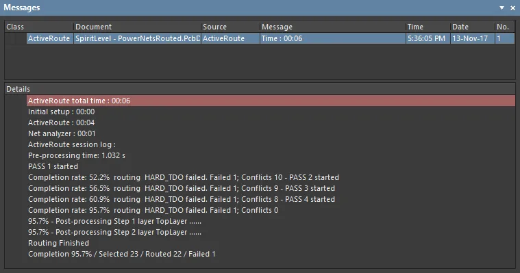
Building Your Proficiency
-
A key ingredient to ActiveRoute proficiency is becoming fluent with the shortcuts. The key sequences you will use most often are:
-
Alt+Click - to select an individual connection line.
-
Alt+Click&Drag - to select connections within an area, drag from right to left to select all touched connections, or left to right to only select what fits inside the selection rectangle. Press Tab to extend the selection to include other connections in the same net(s). The Status bar will display the number of connections just selected until the cursor moves over another object.
-
Ctrl+Click&Drag - to select pads in a component, drag from right to left to select all touched pads, or left to right to only select what fits inside the selection rectangle. Press Tab to extend the selection to include other route objects in the same net(s). Keep pressing Tab to cycle through all possible selection states.
-
Click&Drag - to select existing track segments, drag from right to left to select all touched tracks, or left to right to only select what fits inside the selection rectangle. Press Tab to extend the selection to include other route objects in the same net(s). Keep pressing Tab to cycle through all possible selection states.
-
Include Shift to retain the current selection while performing another selection.
-
Shift+A to ActiveRoute the current selection.
-
Ctrl+Alt+G - to Gloss the current selection.
-
Selection actions are only performed on objects that are visible (except for Ctrl+A):
-
Press Shift+S to cycle in (out) of single-layer mode so only the layer of interest is showing.
-
If the design uses placement rooms, they can be locked as part of their definition in the Design Rules, or they can be hidden to prevent them from being selected/moved during Click&Drag actions. Rooms can be hidden in the View Options tab of the View Configuration panel.
-
Fanout SMD pads. ActiveRoute does not change layers, so you will need to fanout SMD pads. To accelerate the fanout process:
-
While routing a connection, press the / shortcut (numeric keypad) to drop a via and release this connection. Use the 2 shortcut if you do not have a numeric keypad (drops a via without suspending).
-
Copy and paste an existing fanout; the PCB editor will automatically update the net names. This can be done for multiple fanouts.
-
Preserve existing fanouts. ActiveRoute will modify fanouts if it sees a better solution or locks them if you do not want them changed. The easiest way to lock fanouts is to select the fanout tracks and vias (use the Selection Filter at the top of the Properties panel to help with this process), press F11 to open the Properties panel, and enable the Locked checkbox. This will lock all selected objects in a single action.
-
If you use a Route Guide and find that the completion rate is low, it may be that there are too many obstacles along the path and the Guide needs to be wider. Press the Up arrow key to widen the Guide during placement.
-
When ActiveRoute is finished, it applies glossing (if enabled in the PCB ActiveRoute panel). To examine the routes as they were at the completion of ActiveRouting, press Ctrl+Z once to undo the glossing. The Gloss command (Route » Gloss Selected) can be used to smooth out tracks and improve the pad entries of any routing, not just ActiveRoutes. Particular attention has been applied to ensuring high-quality pad entries for differential pairs. To learn more about glossing, refer to the Glossing & Retracing of Existing Routes page.
-
If ActiveRoute does not work, it is usually because the rules are not properly configured. The most common reason for ActiveRoute to fail is not enough room for the track(s) to fit. Check that the rules are appropriate, for example, the default rules that exist in a new PCB file might be too large for a high-density BGA-type design.
-
ActiveRoute observes the routing rules configured for widths, clearances, diff pair gaps, by layer, by room, and by class. ActiveRoute does not route with arcs or any-angle tracks.