Altium Designer Advanced
Go beyond the essentials to
push the limits of your PCB design
Trusted PCB Design Training Courses Backed by Leading Tech and Electronics Companies
Go Beyond the Essentials
with Altium Designer
Take your skills to the next level with expert guidance & custom course offerings
Altium Designer Advanced—available as instructor-led or custom private training—provides experienced users with in-depth instruction on schematic capture, PCB development, project management, and layout configuration. Interactive exercises in a dedicated workspace, along with a pre-training connection, ensure a practical and applied learning experience.
- Hands-on instruction helps you master harness components and understand practical applications
- Learn best practices to streamline your board design and dramatically reduce design errors
- Gain an advanced understanding of Altium Designer’s structure and methods
- Customize Day 3 in Private Training with modules that maximize impact for your team
- Earn a certificate and badge to validate your skills

Advance your design skills by learning from Altium experts!
Training Starts at
Introducing:
Customizable Private Training
Choose your own training experience. After two days of advanced core modules, you’ll customize Day 3 by selecting 8 modules from our expert library of 20—ensuring the training focuses on the skills, workflows, and challenges that matter most to you and your team.
Which 8 modules will your team choose?
Download the Full Agenda

Get Industry-Recognized Credentials
Earn a certificate and digital badge that validates your skills and supports career advancement.

Tackle Complex Design Challenges
Work directly with instructors to explore advanced concepts and apply solutions to your team’s real-world projects.

Learn Industry-Standard Techniques
Master proven methods in a live, guided format to sharpen professional competence and design precision.

Train with Industry Experts
Gain hands-on guidance from Altium experts who bring deep industry knowledge and practical design experience to every session.
Choose Training to Match
Your Learning Style
USD 2,396
Hours of Training: 24
Downloadable Activities: 196
Requirements:
A stable internet connection
Access to an Altium Account
- Latest Altium Designer installation
This interactive, project-based course ensures attendees gain both the knowledge and practical skills needed to efficiently use Altium Designer and leverage Altium Platform capabilities in their electronic design workflows.

Course Agenda
Getting Started with the Altium Workspace
0.5 HoursKey Topics Covered:
- Connecting to the Training Workspace - Access and establish a connection to the training Workspace.
- Workspace Structure Overview - Get acquainted with the organization and folder structure within the workspace to streamline navigation and project management.
- Training Project Management - Understand how training projects are organized, stored, and handled throughout the course.
Templates for Project Efficiency
2.5 HoursKey Topics Covered:
- Draftsman Template Creation - Learn how to create customizable templates in Draftsman, enabling standardized and efficient PCB documentation.
- Using a Draftsman Template for PCB Documentation - Apply Draftsman templates to quickly generate consistent PCB documentation for any project.
- Project Template Creation - Develop reusable project templates that save time and ensure consistency across multiple projects.
- Creating a New Project from a Template - Use established templates to rapidly initiate new projects with predefined settings and configurations.
- Design Reuse Block Creation - Discover how to create reusable design blocks for components or design elements that appear frequently across projects.
- Using Design Reuse Blocks in a Design - Implement design reuse blocks into your projects to maintain consistency and efficiency.
Schematics
2.5 HoursKey Topics Covered:
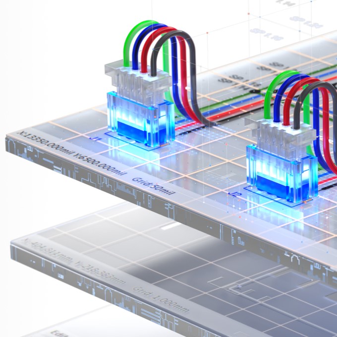
- Use Cases for Signal Harnesses - Understand different scenarios and applications for implementing signal harnesses in designs.
- Creation of Signal Harnesses - Learn the step-by-step process of creating signal harnesses to manage connections efficiently.
- Placing Signal Harnesses - Discover best practices for placing signal harnesses within your schematic for optimal organization and clarity.
- Connection Based on Signal Harnesses - Explore how to establish connections using signal harnesses to streamline design workflows.
- Pin Swapping Configuration - Configure pin swapping options to enhance flexibility in your designs.
- Pin Swap on PCB - Learn how to implement pin swaps on the PCB to accommodate design changes.
- Sync PCB and Schematic After a Pin Swap - Understand the process of synchronizing the PCB with the schematic after making pin swaps to ensure design integrity.
- Creating True Variants - Gain insights into creating true variants within your project to support different design configurations.
- Creating a Variant with Alternative Components - Explore how to create variants that include alternative components for increased design flexibility.
- Variant and the Documentation of the Project - Learn to document variants accurately within your project to maintain clarity and organization.
- Sync PCB After Setting Up a Variant - Discover the steps to synchronize your PCB layout after establishing a variant to ensure all elements are correctly aligned.
- Variant Information and the PCB - Understand how variant information affects the PCB and how to manage it effectively throughout the design process.
PCB Configuration
1 HourKey Topics Covered:
- Clearance Checking: 2D to 3D - Explore methods for checking clearance between components and traces as you transition from 2D to 3D views, ensuring that designs meet physical space requirements and compliance.
- Creating a Board Shape from a 3D Model - Learn how to define and create a custom board shape directly from a 3D model, integrating advanced design techniques for more complex geometries.
Additional Modules
The course also covers the following topics:
- PCB Design Techniques
- High-Speed Designs and the Constraint Manager
- Methods to Replicate Schematic and PCB Layout
- Special Features in PCB Design
Download the full agenda for a complete list of modules and topics.
Choose an Upcoming Course Date
for Live Training Delivered by Altium Instructors
Language: English
Region: Americas
Seats Available: 8
Price:
Language: English
Region: EMEA
Seats Available: 6
Price:
Language: German
Region: EMEA
Seats Available: 8
Price:
Language: English
Region: APAC
Seats Available: 12
Price:
Language: Italian
Region: EMEA
Seats Available: 8
Price:
Language: English
Region: EMEA
Seats Available: 12
Price:
Language: English
Region: Americas
Seats Available: 8
Price:
Language: German
Region: EMEA
Seats Available: 12
Price:
Language: French
Region: EMEA
Seats Available: 11
Price:
Language: Japanese
Region: APAC
Seats Available: 12
Price:
Language: English
Region: India
Seats Available: 14
Price:
Language: English
Region: EMEA
Seats Available: 12
Price:
Language: English
Region: Americas
Seats Available: 11
Price:
Language: German
Region: EMEA
Seats Available: 12
Price:
Language: English
Region: EMEA
Seats Available: 12
Price:
Language: Italian
Region: EMEA
Seats Available: 12
Price:
Language: French
Region: EMEA
Seats Available: 12
Price:
Language: Spanish
Region: EMEA
Seats Available: 12
Price:
Language: English
Region: Americas
Seats Available: 12
Price:
Language: German
Region: EMEA
Seats Available: 12
Price:
Language: Japanese
Region: APAC
Seats Available: 12
Price:
Language: English
Region: EMEA
Seats Available: 12
Price:
Language: English
Region: India
Seats Available: 15
Price:
Language: German
Region: EMEA
Seats Available: 12
Price:
Language: English
Region: Americas
Seats Available: 11
Price:
Language: English
Region: APAC
Seats Available: 12
Price:
Language: Italian
Region: EMEA
Seats Available: 12
Price:
Language: English
Region: EMEA
Seats Available: 12
Price:
Language: English
Region: Americas
Seats Available: 12
Price:
Language: German
Region: EMEA
Seats Available: 12
Price:
USD 18,000
Hours of Training: 3 days, including breaks
Downloadable Activities: 196
Private training offers personalized, instructor-led guidance from Altium experts, delivered either onsite or online at your team’s convenience. The Altium Designer Advanced Private Custom program includes two days of core advanced modules plus a fully customizable Day 3. Your team selects 8 specialized modules from our expert library to ensure training directly addresses your most pressing design challenges.
Requirements:
A stable internet connection
Access to an Altium Account
- Latest Altium Designer installation
This interactive, project-based course ensures attendees gain both the knowledge and practical skills needed to efficiently use Altium Designer and leverage Altium Platform capabilities in their electronic design workflows.
*Pricing includes 10 seats; additional seats available for purchase (up to 15).
Course Agenda
Core Modules - Days 1 & 2
16 HoursHands-on advanced techniques every professional designer must master—delivered to all participants over two days.
Key Learnings:
Multi-Board & Multi-Channel Design – Create hierarchical assemblies, manage inter-board connections, and implement room-based PCB layouts with synchronized channels.
Advanced Routing Techniques – Apply differential pair routing with impedance control, length tuning, and pin swapping to ensure high-speed signal integrity.
Design Efficiency & Reuse – Build reusable design blocks, replicate layouts, and streamline multi-variant configurations across projects.
Rule Management & Validation – Develop complex design rule queries, integrate schematic/PCB constraints, and implement systematic design review workflows.
Project Management & Release – Control BOM variants and lifecycles, configure project release workflows, and manage documentation and version control with workspace integration.
Download the full agenda for a detailed module list.
Open PDF
Custom Modules - Day 3
8 HoursDay 3 is built around flexibility, choose 8 of 20 specialized modules to sharpen skills in the areas that matter most to your team—from compliance and signal integrity to rigid-flex and manufacturing-ready design.
Key Learnings:
3D & Rigid-Flex Design – Validate 3D clearances, define board shapes from CAD models, design embedded board arrays, and optimize rigid-flex stackups and bend areas.
Pads, Vias & HDI Techniques – Create custom pads, apply via templates, stitching, and back drills, and implement HDI structures for high-speed, multilayer designs.
Routing & Connectivity – Optimize BGA fanout and escape routing while integrating signal harnesses for full system coordination.
Documentation & Manufacturing Prep – Standardize outputs with Draftsman and project templates, edit CAM files, and prepare data for efficient production.
Design Rules & Verification – Apply creepage and clearance constraints, perform design comparisons, and ensure accuracy, compliance, and manufacturability.
Collaboration & CoDesign – Establish team-based workflows and collaborative methods for managing complex PCB projects.
Download the full agenda for a detailed module list.
Open PDF

Sign up for Private Training
Private training is perfect for design teams and offers you the comfort of confidentiality of any designs and discussions covered during sessions. Private training is available to be delivered onsite or via online instruction.
Meet Your Instructors
Learn from industry-leading experts. Altium instructors are seasoned engineers with deep PCB experience and the latest Altium Designer knowledge. Their insights and real-time feedback during the course are invaluable.
Michael Heil
Instructor

Michael Heil is an expert PCB designer and Altium Certified Trainer with over a decade of experience in electronics design. His deep understanding of Altium Designer's advanced features and practical design techniques makes him a valuable resource for engineers looking to elevate their skills.
Kristen Aguiar
Instructor

Kristen Aguiar is a seasoned PCB designer and Altium Certified Trainer, with extensive experience in complex electronics systems. Known for her hands-on teaching style, Kristen excels at breaking down advanced Altium Designer features and delivering practical solutions that help engineers streamline their design process.
Tally Kainth
Instructor

Tally Kainth is an accomplished electronics engineer and Altium Certified Trainer with a strong background in PCB design and development. With a focus on real-world applications, Tally's training sessions offer practical insights into using Altium Designer's latest tools to create high-performance designs efficiently.
Tomas Chester
Instructor

Tomas Chester is an expert in PCB design with over 15 years of experience, specializing in high-speed and high-density designs. As an Altium Certified Trainer, Tomas brings a wealth of knowledge and industry experience to his sessions, providing engineers with actionable insights and advanced techniques in Altium Designer.
Showcase Your Skills with
Altium Course Certificates & Badges
Top Electronics Companies Worldwide Prefer
Working with Altium-Experienced Designers
Earn Your Course Certificate
Stand out in the industry with an official Altium Designer certificate that validates your PCB design knowledge.
Looking to upskill?
Book a private, instructor-led, or on-demand course today.


Skilled PCB Designers Refine Their Craft Through Altium Training
G2 users consistently rate Altium as their top choice for easy-to-use PCB design.
Ready to take the next step in your career? Book your training today!
Altium Training
Loved by Learners, Trusted by Pros
Join a growing community of successful PCB design students.

94% of customers report they are likely or extremely likely to recommend Altium’s Instructor-led training to a friend.

Careers in PCB Design are Growing! Nearly 78% of the electronic design workforce is projected to retire in the next 15 years.
Printed Circuit Design & Fab (PCD&F) magazine
Are you ready to take your career to the next level?
Ready for More?