Chinese - Translation is available for Altium Designer 24:
Go to the pageIn the PCB editor, the connectivity between the nodes in a net is represented by a series of point-to-point connection lines, which are collectively referred to as the ratsnest. When the design is transferred from the schematic (Design » Update PCB), the components are placed on the PCB design space and the connection lines are displayed (as thin, solid lines).
Within an individual net, the connection lines join all of the nodes in that net. The pattern, or order they connect, is called the Net Topology, which is discussed below.
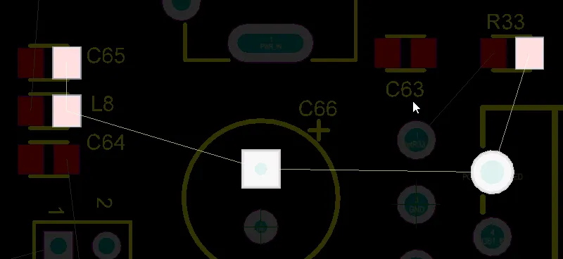
The nodes in the net are connected by connection lines in accordance with the applicable Routing Topology rule (the default is Shortest).
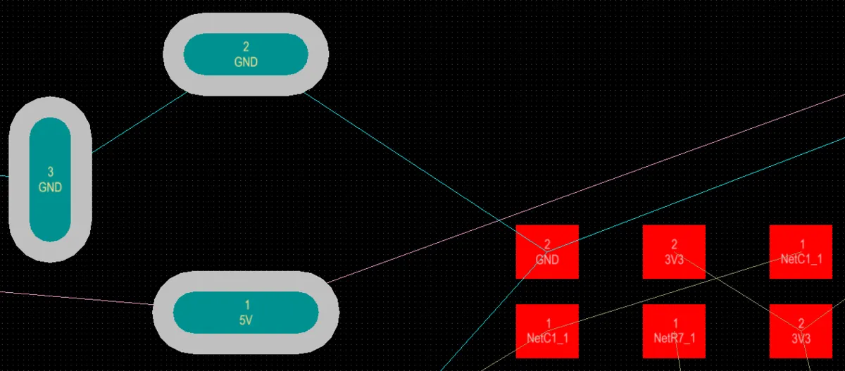
In this design, the GND and 5V nets use a different color for their connection lines.
As well as being a helpful guide during component placement, the connection lines are also a valuable guide during interactive routing and autorouting.
The PCB editor includes a net analyzer that constantly monitors the location of all objects in the design space and updates the connection lines when any net-type object is edited (including an object being moved). For example, when a component is moved, the far end of each connection from that component can jump from one target pad to another target pad, as they are updated to maintain the topology defined by the applicable design rule. An example of this is shown for the GND net in the video below; this net has a topology of shortest.
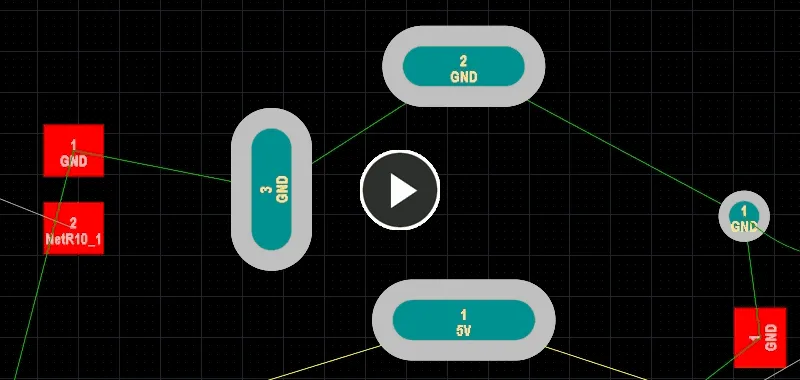
Note how the GND connection lines jump around as the resistor is moved, automatically being rearranged to keep the shortest overall connection length.
Finding a Net on the Board
An un-routed board can appear intimidating - a mass of connection lines crisscrossing all over the board. A good approach to routing is to work from the schematic, where you can easily locate important components and critical nets. You can cross-select and cross-probe directly from the schematic components and nets, highlighting the equivalent item on the PCB. Learn more about Working Between the Schematic and the Board.
A valuable feature is the PCB editor's ability to mask or dim objects in the design space. This filtering feature will fade out everything, except the object(s) that pass through the filter. The image below shows a single net has been selected, with the filtering system set to Dim all objects that do not pass the filter.
To explore this, set the PCB panel to Nets mode, this will display a list of nets on the board. Use the dropdown to set the filter mode to Dim or Mask, then enable the Select and Zoom options, as shown in the image below.
As you click on a net name in the panel the design space display will change, zooming to show the nodes in the net, and fading out everything except the pads and connection lines in the net - effectively pulling that net out from the rest of the board. Note that even when you click in the workspace the filter remains, the chosen net remains clearly visible, making it easy to examine or route.
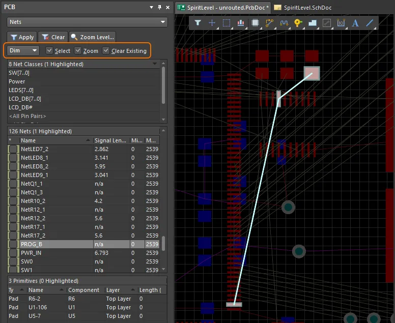
Use the filter feature to make it easier to find a net or net class.
Click the Clear button at the top of the PCB panel to clear the filter and restore the entire design space to normal brightness (or press the Shift+C shortcut).
Note that as well as an individual net, you can filter out a class of nets (if any classes are defined) in the Net Classes section of the panel, and also interactively select multiple nets (hold Ctrl as you click in the PCB panel to select a net name).
Connection line(s) of a specific net can be selected to display their properties in the Properties panel by using the IsConnection And InNet('<NetName>') query in PCB Filter panel (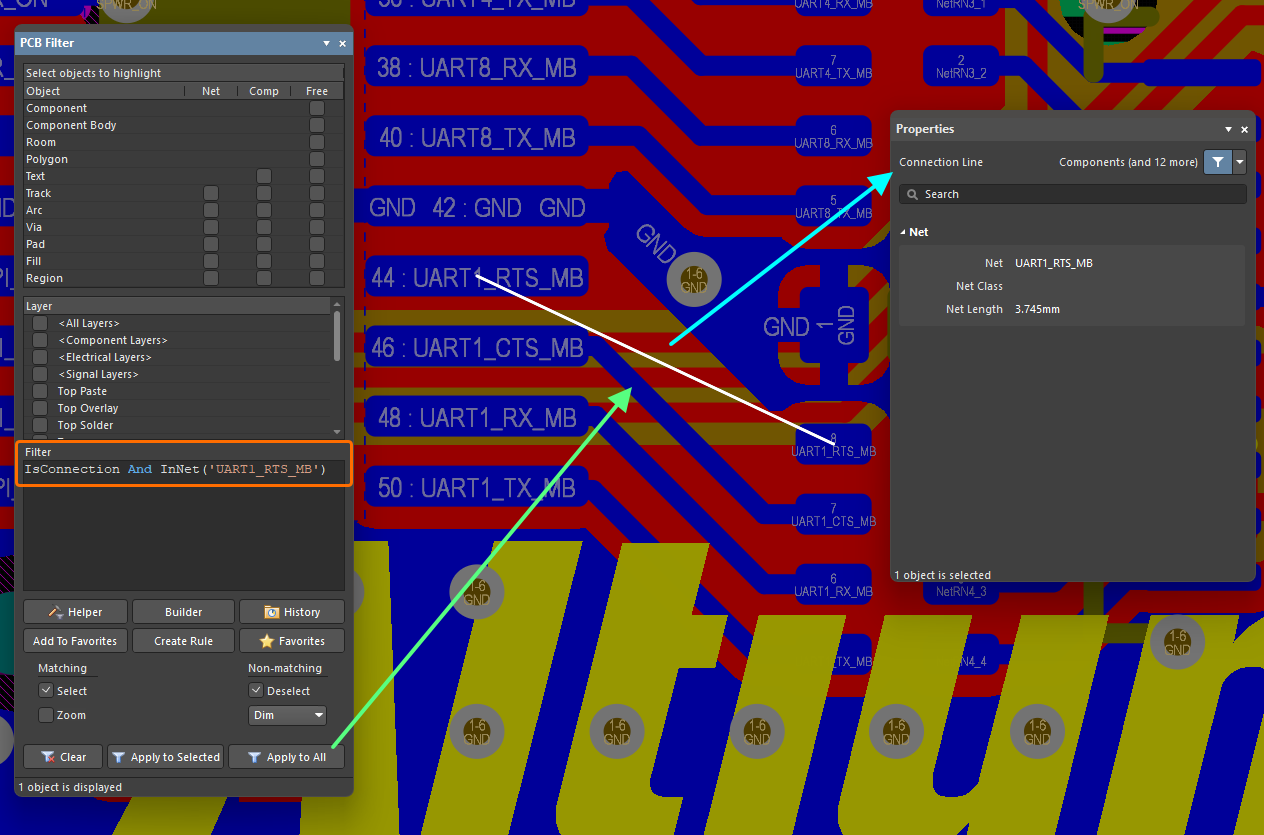 ).
).
For more information about working with the query language and the Filter panels, refer to the Working with the Query Language page.
Browsing Nets
In the PCB panel's Nets mode, its three main regions change to reflect the net hierarchy of the current PCB design (in order from the top):
-
Net Classes, as defined by the board.
-
Individual member Nets within a class.
-
Individual Primitives within a Net (pads, vias, tracks, and fills).
Net Classes
In the top region of the panel (Net Classes), right-click on a net or net item entry then choose Properties from the subsequent menu (or double-click on the entry directly) to access the Edit Net Class dialog in which you can view or edit the net membership of the class, rename it, or add additional classes.
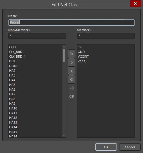
You can also manage net classes using the following commands of the Design » Netlist sub-menu of the main menus or the Net Actions sub-menu of the right-click menu of selected net object(s):
-
Create NetClass from Selected Nets - this command is used to create a new net class from two or more selected nets in the design space. After launching the command, the Object Class Name dialog will open. Use this to specify the required name for the new Net Class. After clicking OK, the net class will be created and the selected nets will be added as members.
-
Add Selected Net(s) to NetClass - this command is used to add one or more selected nets to an existing net class. After launching the command, the Choose Net Class dialog will open. This dialog lists all of the existing net classes. Select the target class then click OK. The net(s) will be added as members of that class.
-
Remove Selected Net(s) From NetClass - this command is used to remove one or more selected nets from an existing net class. After launching the command, the Choose Net Class dialog will open. This dialog lists all of the existing net classes. Select the target class then click OK. The net(s) will be removed as members from that class.
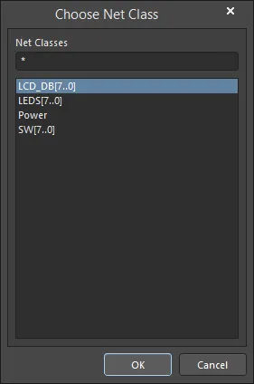
The Choose Net Class dialog
The easiest and quickest way to select nets (or rather the objects thereof) in the design space is to use the PCB panel configured in its Nets mode. Choose <All Nets> in the Net Classes region then select the required net(s) in the Nets region. Filtering is applied to the design workspace, leaving just those electrical objects associated with the chosen net(s) selected (make sure the Select option is enabled on the panel and also that the highlighting mode is either set to Mask or Dim). This makes it especially easier to distinguish the objects if using the right-click method of access.
Nets
The middle region of the panel displays nets from the Net Class(es) selected in the region above.

The following information is listed with each Net by default:
-
 - this feature has two functions:
-
Color background - the color assigned to the net. This color is always applied to the net's connection lines. It can also be applied to that net's routing using the net color display override feature. Double-click to edit the color for this net, or right-click to edit the color for all currently selected nets.
-
checkbox - check this to apply the color to the routing (enable the net color display override feature) for this net. Right-click to enable (or disable) the display override feature for all currently selected nets. Press F5 to enable/disable net color display override in the design space.
► See Net Color Override - Displaying the Net Color on Routed Nets to learn more.
-
Name - name of the net.
-
Node Count - the total number of pads in this net.
-
Routed Length - the sum of the lengths of the placed track and arc segments that form the routing, plus the vertical distance traversed through vias (see note below). The routed length calculator does not attempt to resolve overlapping track segments or routing wiggles inside pads.
-
Signal Length - accurate calculation of the total node-to-node distance. Placed objects are analyzed to: resolve stacked or overlapping objects and wandering paths within pads; and via lengths are included. If the net is not completely routed the Manhattan (X + Y) length of the connection line is also included.
If there are Length design rules configured, the routed state of each net targeted by the rule is also colored, highlighted in yellow if the route length < rule minimum, clear if the net passes the rule, or red if the route length > rule maximum.
The following notes apply to Signal Length calculations:
-
Resolves overlaps and wiggles inside pads.
-
Handles routing paths created with objects other than tracks and arcs (e.g., a region or a fill).
-
Includes vertical distances through vias (see note below).
-
Includes the Total Pin/Package Length for this net.
-
Includes the Unrouted (Manhattan) length for this net.
-
Failure to comply with applicable Length/Matched Length design rules is flagged by the signal length being displayed on a colored background: signal lengths that are too short in yellow, signal lengths that are too long in red.
► See Length Tuning to learn more about how the Length and Matched Length design rules are applied.
-
A signal is a point-to-point entity; for this reason, only nets with two nodes will show a Signal Length in the Nets mode of the panel (nets with other Node counts will display 0). For nets with more than two nodes, define xSignals to calculate their signal length.
► See PCB - xSignals.
► See Defining High Speed Signal Paths with xSignals to learn more about xSignals.
-
Total Pin/Package Length - the sum of all the Pin Package Length values in all pads in that net. This value is defined as a property of the PCB pad and can also be specified in the schematic pin.
-
Unrouted (Manhattan) - the vertical plus horizontal (X+Y) distance of all unrouted sections.
Right-click in the region then use the Columns sub-menu to add the following columns:
-
Min/Max - settings from the applicable Length and Matched Length design rules. If there is no applicable rule(s) defined, the internal defaults of Min=0mil and Max=99999mil are used.
► See Length Tuning to learn more how the Min and Max settings are derived from the Length and Matched Length design rules.
-
Estimated Length - this is the Routed Length plus the length of connection lines for any section still to be routed. It does not use the Manhattan length for the unrouted portion; instead it uses the direct point to point distance.
-
Delay - the time it takes for a signal to propagate along that route.
Vertical distance through a via - the vertical distance a signal travels through a via is the sum of all layer thicknesses (copper and dielectric) between the start and stop layers copper layers, plus half the thickness of the start layer and half the thickness of the stop layer.
The length and delay for a net that is part of a defined Supply Nets design rule (or part of a net class used with such a rule) are not calculated (values are shown as n/a in the panel).
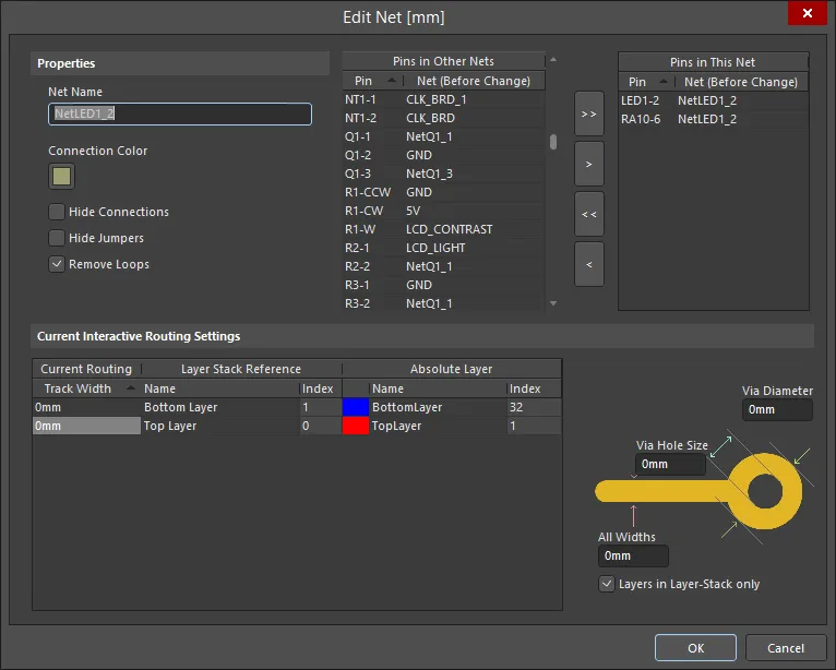
Double-click on the entry for a specific net in the Nets region (or right-click on the net entry then choose the Properties command from the context menu) to open the Edit Net dialog from which you can modify the properties of the net.
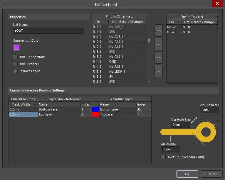
Options and Controls of the Edit Net Dialog
Properties
-
Net Name - rename the net, if desired.
-
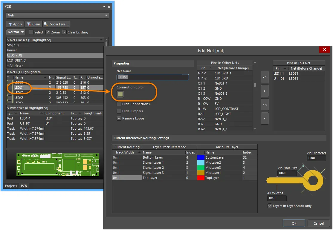
Connection Color - click to open the Choose Color dialog to choose a connection color for the specified net. This net color can also be applied to the routed net, when the Net Color Override feature is enabled (press F5).
-
Hide Connections - enable to hide connection wires.
-
Hide Jumpers - enable to to hide jumpers or short connections between routed segments.
-
Remove Loops - enable to automatically remove any redundant loops that are part of this net.
Pins in Other Nets
This is a list of all the pins on the PCB. Pins that are currently assigned to a net include their net name in brackets. Select the pins you wish to add to the net being edited. Use the Shift and Ctrl keys to select multiple pins. Use the control buttons to move selected pins into the current net list or right-click to remove selected pins from the list using the context menu.
Buttons
-
 - use to add all Pins in Other Nets to Pins in This Net.
-
 - use to add the selected Pins in Other Nets to Pins in This Net. Use the Shift and Ctrl keys to select multiple pins.
-
 - use to move all Pins in This Net to Pins in Other Nets.
-
 - use to move the selected Pins in This Net to Pins in Other Nets. Use the Shift and Ctrl keys to select multiple pins.
After moving a pin from the Pins in Other Nets list to Pins in This Net list, you may right-click on the moved pin and select the Remove One command to move it back to the Pins in Other Nets list.
Pins in This Net
Lists all pins in this net. Select the pins you wish to remove from this net. Use the Shift and Ctrl keys to select multiple pins. Use the control buttons to move selected pins out of the current net list or right-click and use the context menu to remove selected pins.
Current Interactive Routing Settings
Grid
The grid region lists any current settings for interactive routing.
-
Track Width - lists the track width field of the current interactive routing settings, which is editable and may be changed to your preference and/or design requirements.
-
Name - lists the Current Routing, Layer Stack Reference, and Absolute Layer.
-
Index - lists the index number.
Diagram
-
Via Hole Size - this represents the current via hole size's user choice value that is stored in the net. This dialog provides a way to modify the current values for the current interactive routing settings. If the values are zero, the user choice values are not being sourced from this dialog and the last used value for this board will be used.
-
Via Diameter - this represents the current via size's user choice value that is stored in this net. This dialog provides a way to modify the current values for the current interactive routing settings. If the values are zero, the user choice values are not being sourced from this dialog and the last used value for this board will be used.
-
All Widths - this is the current routing and their layer reference values that represent the current user choice values that are stored in the net. It provides a way to modify the current values for the current interactive routing settings. If the values are zero, the user choice values are not being sourced from this dialog and the last used value for this board will be used.
-
Layers in Layer-Stack only - enable to apply the via parameters for layers in the layer-stack only.
The
Edit Net dialog can also be accessed from the design space by right-clicking over a placed design object then choosing the
Net Actions » Properties command from the context menu. The dialog will open for the parent net to which the object is associated.
Primitives
The display/inclusion of each net item type in the bottom Primitives region of the panel is dependent on whether the corresponding option for each has been enabled on the right-click menu, accessed from either the Nets or Primitives regions.

Right-click on a net or net item entry to select the included items.
Note that the Primitives list right-click context menu also offers the option to create an xSignal between two selected items. See PCB - xSignals for more information.
Managing the Display of the Connection Lines
Related page: Your View of the PCB
The connection lines are a valuable aid to help with placing and orienting the components and to guide you during routing. However, their presence can also create a lot of visual clutter. To help with this, the PCB editor includes the features described below to help the designer manage the display of connection lines.
Changing the Connection Line Color
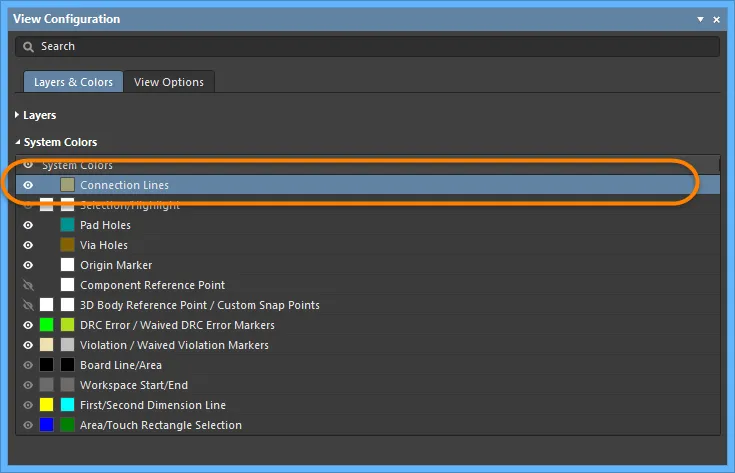
When the design is transferred from the schematic into the PCB workspace, default layer and color settings are applied. As part of this process, all of the connection lines are assigned the default Connection Lines color, as defined in the System Colors section of the Layers & Colors tab of the View Configuration panel (L shortcut). View configurations are available for use in both 2D and 3D workspaces, and can be saved and re-applied (View Options tab of the View Configuration panel).
An easy way to make important nets stand out during the routing process is to change the color of their connection lines. To do this, double-click the net name in the PCB panel to open the Edit Net dialog, where you can edit the connection line color (set the panel to Nets mode).
Alternatively, to change the color of one or multiple nets, first select the required nets in the PCB panel, then right-click on a selected net and choose the Change Net Color command.
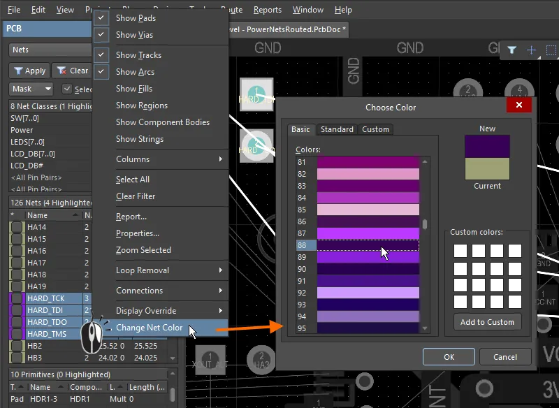
In the PCB panel, right-click on selected nets to change the color of their connection lines.
Displaying Connection Lines using the Layer Colors
As well as assigning the connection line color for individual nets, you can also display the connection lines using the colors of the start and end layers that the connection line travels between. If a connection line travels from an object on one layer to an object on a different layer, the connection starts in the color of the layer of the first object, then morphs to the color of the layer it ends on, as it approaches the object on that layer (as shown in the image below).
Note that this gradient color override is only applied to nets that travel from one layer to another; if the connection starts and ends on the same layer, it retains its defined color.
This feature is helpful when you are routing a multi-layer board, as it indicates the target layer that the connection being routed, must go to. Note that color morphing is only applied to connections that travel from one layer to another, if the connection starts and ends on the same layer it retains the assigned net color.
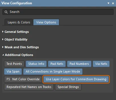
To use the layer color feature, enable the Use Layer Colors for Connection Drawing option in the View Options tab of the View Configurations panel, as shown below.
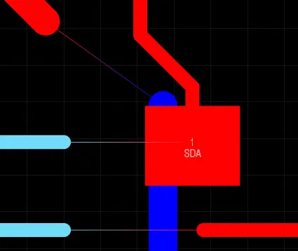
Connection lines can be displayed using their start-and-end layer colors. In the image on the right, a number of nets have had routing segments removed to show how the connection lines display.
Displaying Connection Lines in Single Layer Mode
A multi-layer board is visually dense, making it difficult to interpret what is going on. To help with this, you can easily switch the layer display from the enabled layers to Single Layer mode, by pressing the Shift+S shortcut.
Normally, when you do this, all connection lines that do not either start or end on the current layer are also hidden, as it is assumed that they are not relevant. To always display the connection lines, enable the All Connections in Single Layer Mode option in the View Options tab of the View Configurations panel, as shown below.
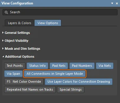
Control the display of connection lines in Single Layer mode.
Hiding/Displaying Connection Lines
As an alternate to filtering nets via the PCB panel, you can completely hide one, many, or all of the connection lines. There are a number of commands to control the display of connection lines in the View » Connections submenu. You can also access these commands while you are working by pressing the N shortcut key. Use the available commands to:
-
All of the available commands have accelerator keys, making it an efficient method of performing such tasks as hiding all connection lines (N, H, A), then displaying the connection lines for a specific net (N, S, N).
-
During component moves, all connection lines are automatically hidden. You may cycle through the display of these connection lines while moving a component. To do so, press the N key while in movement mode. When pressing the N key in movement mode, the Heads Up display cycles between displaying Breaks, Hidden, or Pad To Pad, depending on which connection you'd like to display.
Net Topology
The pattern or order that the nodes in the net are connected to each other is called the net topology. Net topology is controlled by the applicable Routing Topology design rule, which defaults to a topology of Shortest. Shortest means the nodes in the net are connected to each other in a pattern that gives the shortest overall connection length for that net. This overall length is monitored as you move a component, and the pattern of the connection lines will change dynamically to keep the overall length shortest. This can be observed in the animation shown above, where the lines connecting downward from the bottom of the moving component jump as the component is being moved - this happens each time one of the connected pads moves closer to another pad in their net.
Applying a Pre-defined Topology using the Routing Topology design rule
Additional Routing Topology design rules can be created to configure a net (or net class ) to use a different topology. To demonstrate this, in the images shown below the default topology rule is shown on the left, and that same net with a new routing topology of Starburst having been applied is shown on the right. In a Starburst topology, the connections radiate from the pad with an Electrical Type of Source (the default type for all pads is Load).
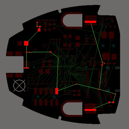
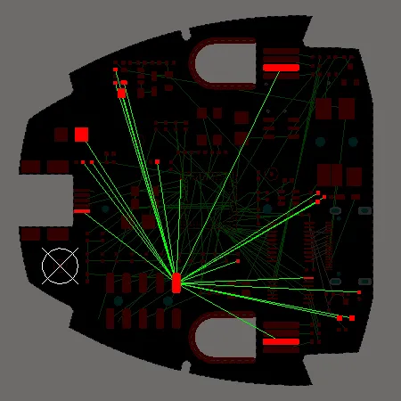
For the default topology, the connection lines are placed to give the shortest overall connection length. In the Starburst topology, the connection lines all radiate from a Source pad.
Applying a Custom Topology
Within an individual net, the connection between two nodes is referred to as a From-To. To control the path of the connection lines down at the individual pin-to-pin level, you can manually define From-Tos within a net, effectively creating a custom net topology.
From-Tos are defined by setting the PCB panel to From-To Editor mode. The process of defining a From-To is to select two Nodes on Net in the panel, and click the Add From To button. To clearly identify From-Tos in the design space, they are shown as a dashed line instead of a solid line.
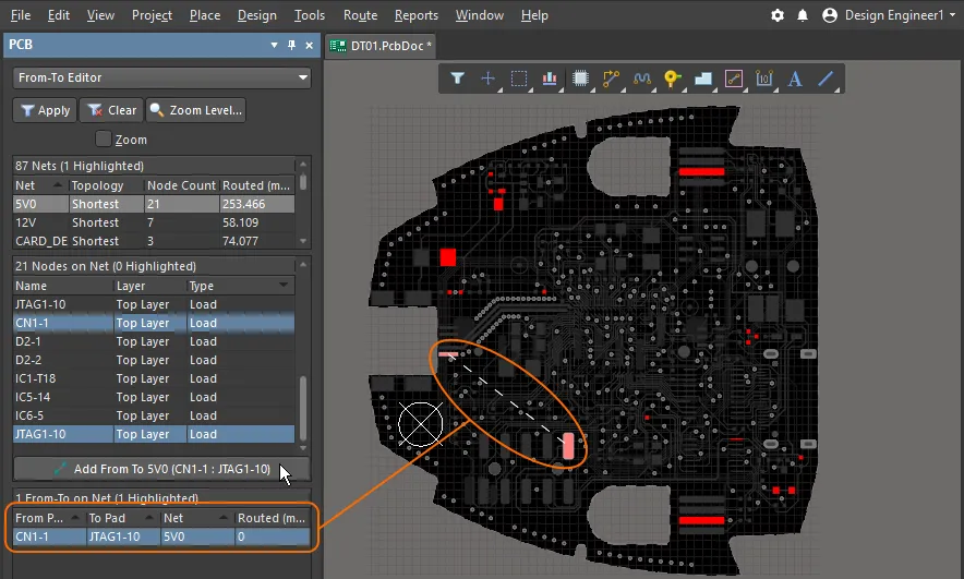
A From-To has been defined between 2 pads, note how the From-To line is displayed as dashed rather than solid.
When the PCB panel is in From-To Editor mode, all of the connection lines that are not From-Tos, are hidden.
The PCB panel’s From-To Editor mode is divided into three sections:
-
Nets
-
Nodes of the selected net
-
From-Tos on Net
As you click on a net entry, all of the nodes on that net will be loaded into the middle region of the panel. Double-clicking on a net entry will open the Edit Net dialog in which you can edit the properties of the net, including node membership.
Adding From-Tos
To add a user-defined From-To between two nodes in a selected net, select the two nodes in the Nodes on Net region of the panel then click the Add From To button.
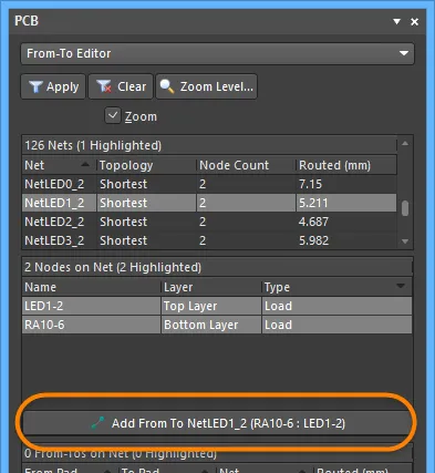
You can select the two nodes (pads) for a From-To directly within the design space. As you select a node, its corresponding entry in the Nodes on Net region of the panel will become selected.
The newly added From-To will appear listed in the From-To on Net region of the panel and appears in the design space as a dotted line between the two nodes.
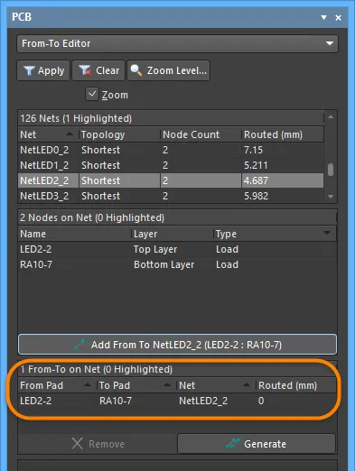
A new From-To has been created on the net.
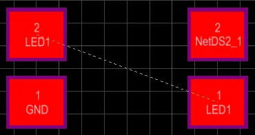
A user-defined From-To in the design space.
To remove a From-To, select its entry in the From-To on Net region of the panel then click the Remove button.
Choosing a Predefined Topology
The topology of a net is the arrangement or pattern of the pin-to-pin connections. By default, pin-to-pin connections of each net are arranged to give the shortest overall connection length.
A topology is applied to a net for a variety of reasons: for high speed designs where signal reflections must be minimized, the net is arranged with a daisy chain topology; for ground nets, a star topology could be applied to ensure that all tracks come back to a common point. You can either create dedicated From-Tos for node pairs in a net or you can choose to generate From-Tos for the net based on one of the predefined routing topologies available.
The following topologies are available and can be accessed from the From-To on Net region of the panel by clicking the Generate button:
-
Shortest - this topology connects all nodes in the net to give the shortest overall connection length.
-
Daisy Simple - this topology chains all the nodes together, one after the other. The order they are chained is calculated to give the shortest overall length. If a source and terminator pad are specified, then all other pads are chained between them to give the shortest possible length. If multiple sources (or terminators) are specified, they are chained together at each end.

-
Daisy Balanced - this topology divides all the loads into equal chains, the total number of chains equal to the number of terminators. These chains then connect to the source in a star pattern. Multiple source nodes are chained together.

-
Daisy Mid-Driven - this topology places the source node(s) in the center of the daisy chain, divides the loads equally and chains them off either side of the source(s). Two terminators are required, one for each end. Multiple source nodes are chained together in the center. If there are not exactly two terminators, the Daisy-Simple topology is used.

-
Starburst - this topology connects each node directly to the source node. If terminators are present, they are connected after each load node. Multiple source nodes are chained together, as in the Daisy Balanced topology.
A pad can be defined as a Source, Terminator or Load by changing the entry for the Electrical Type field accordingly in the Pad mode of the Properties panel. Access to the Pad mode of the Properties panel is made by double-clicking on the entry for the pad in the Nodes on Net region.
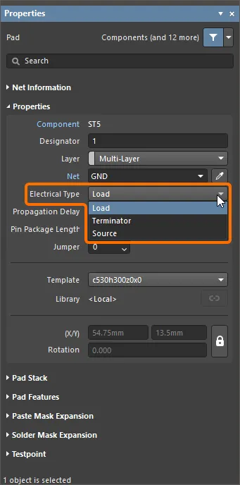
Setting a pad's Electrical Type to Source in the Pad mode of the Properties panel.
When you change the electrical type for a pad to Source or Terminator, an "[S]" or "[T]" will be placed in the design space to distinguish it.
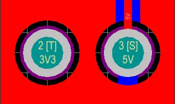
Notes
-
A system-generated connection line does not appear in the design space as a separate entity. Only the associated pin-to-pin connection line for the From-To is displayed, which is used for interactive routing/Autorouting guidance.
-
A user-defined From-To appears in the design space as a dotted line, separate and distinct from the pin-to-pin connection line that is also displayed when the FromTo is added. The user-defined From-To line controls where the associated pin-to-pin connection line starts and finishes. This is best demonstrated by example. Consider a user-defined From-To added between the logically connected pins of two components. A connection line is also added and displayed (PCB panel configured in Nets mode):
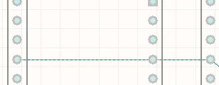
-
The pin-to-pin connection line - used for routing purposes - conceals the presence of the distinctly separate user-defined From-To line. However, as you start to route the connection, you can see the distinct and separate nature of the two lines:
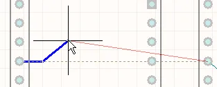
-
If the routing is now suspended, the net analyzer adds a connection line so as to maintain the required topology, shown as a dotted line (called a Broken Net Marker), indicating that the net should be routed between these two points to maintain the topology determined by the user through the addition of the user-defined FromTo:
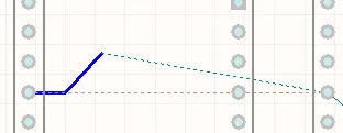
-
If you specify user-defined From-Tos for only part of a net, the PCB editor will set the remaining pin-to-pin connections (system-generated From-Tos) to the Shortest topology.
-
The type of From-To determines how the Connectivity Analyzer treats the connection line in the design space when, for example, a net object is moved or part of a net is manually routed:
-
System-generated From-To - the connection line can be moved as required as part of the net analyzer's re-optimization to keep the default topology of the net (i.e., Shortest).
-
User-defined From-To - if the From-To is not the result of selecting a predefined topology, the connection line is not considered as part of the net analyzer's re-optimization process. If the From-To is part of a predefined net topology (other than Shortest), the net analyzer can include it in re-optimization, as long as the chosen topology is kept.
-
Implementation of custom topologies defined using From-Tos can be checked during the Batch Design Rule Check (DRC) of the Routing Topology design rules applied to corresponding nets. A violation is detected if there is an electrical connection between the pads of a From-To, and the shortest path contains at least one other pad of this net.
❯ ❮
Javascript ID: RoutingTopology_FromTos_AD24_5
|
Two From-Tos are created between three pads – from pad 1 to pad 2 and from pad 2 to pad 3
Routing is created according to the configuration of From-Tos – there is routing between pads 1 and 2 and between pads 2 and 3. No violation of the Routing Topology rule is detected.
Routing is created in a T-branch manner. There are no additional pads in paths according to the From-To configuration, so no violation of the Routing Topology rule is detected.
Routing is created between pad 1 and pad 3 and from pad 2 and pad 3. This routing does not match the From-To configuration because there is an additional pad 3 at the path between pad 1 and pad 2, so a violation of the Routing Topology rule for the From-To between pads 1 and 2 is detected.
|
Violations will not be detected for nets with a large number of pads (more than 20) or primitives (more than 1024).
The Routing Topology DRC support is in Open Beta and available when the PCB.Rules.CheckRoutingTopology option is enabled in the Advanced Settings dialog.
The Netlist Manager
The Netlist Manager dialog accessed by choosing the Design » Netlist » Edit Nets command from the main menus provides controls to effectively manage the netlist for the board. Nets can be added, edited or deleted as required, and the pins (or pads) of the components in those nets also can be edited with respect to their properties. Access to other netlist management tools is also provided through this dialog, including the ability to create the netlist based on connected copper on the PCB and the ability to export the netlist from the PCB.
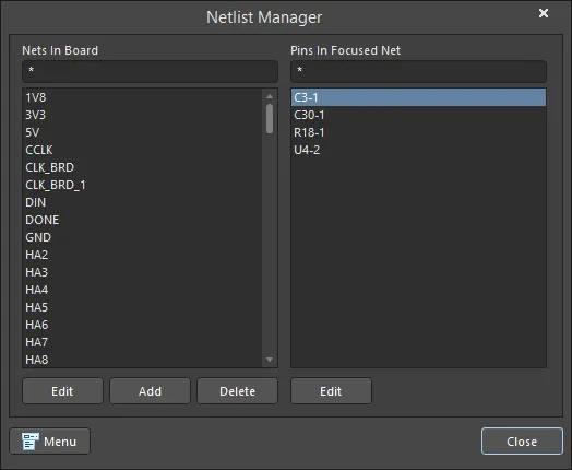 The Netlist Manager dialog
Options and Controls of the Netlist Manager Dialog
-
Nets In Board - this region of the dialog presents all of the nets defined for the board by name. Use the mask field above the list to quickly filter the content.
The mask field is used to filter the list to only show strings that match the mask string. You can use the * (any characters) wildcard in the mask string - for example, "*" to display all nets, or "D*" to display all nets that start with the letter D.
-
Edit - click to access the Edit Net dialog in which you can view and modify the properties of the currently selected net (or focused net, when multiple nets are currently selected in the list. The focused net is presented with a dotted border).
-
Add - click to add a new net for the board. The Edit Net dialog opens in which you can define the properties of the net. The initial, default name for the new net is NewNet; change as required.
-
Delete - click to delete the currently selected net(s) from the board. A confirmation dialog will appear; click Yes to continue with the removal.
Standard multi-select techniques (Ctrl+click, Shift+click, Click&drag) are supported in the Nets listing.
-
Pins In Focused Net - this region presents all of the pins (component pads) associated/belonging to the currently selected/focused net. For each entry in the list, the identifier for the pin is shown in the format <ComponentDesignator>-<PinDesignator>. Use the mask field above the list to quickly filter the content.
The mask field is used to filter the list to only show strings that match the mask string. You can use the * (any characters) wildcard in the mask string -for example, "*" to display all pins in the selected/focused net, or "U*" to display only those pins associated with components whose designator start with the letter U.
-
Edit - click to access the Pad dialog in which you can view and modify the properties of the currently selected pin (pad).
-
Menu - click to access a menu offering the following commands:
-
Add Net - use to add a new net for the board. The Edit Net dialog opens in which you can define the properties of the net
-
Delete Net - use to delete the currently selected net(s) from the board. A confirmation dialog will appear; click Yes to continue with the removal.
-
Update Free Primitives From Component Pads - use to resynchronize the net name of the routing primitives to the net name to which the pads they connect. After launching the command, a confirmation dialog appears asking whether you wish to update free primitive nets with the component-pad nets. After clicking Yes, starting from each pad, the connected copper is selected and the net name of each primitive set to match that of the pad.
This operation does not affect the internal PCB netlist.
-
Clear All Nets - use to clear all nets from the current design document, essentially flushing the internal PCB netlist. This may be desirable if you have changed net information in the source schematic documents and you want to fully resynchronize your PCB with the source schematic netlist information. After launching the command, a confirmation dialog will appear alerting you to the fact that this operation will clear all net information from the PCB. After clicking Yes, all net information will be removed. Any routed track will remain routed, but will have a No Net assignment. Any unrouted logical connections will be removed.
-
Export Netlist From PCB - use to export to file the internal PCB netlist for the current document. After launching the command, a confirmation dialog will appear asking if you wish to export the netlist from the PCB. After clicking Yes, a netlist (Exported <PCBDocumentName>.Net) is created in the same folder as the PCB design document.
-
Create Netlist From Connected Copper - use to create a netlist file based on the connectivity created by the routing in the current design. After launching the command, a confirmation dialog will appear asking if you wish to generate a netlist from the copper on the PCB. After clicking Yes, a netlist (Generated <PCBDocumentName>.Net) is created in the same folder as the PCB design document which automatically opens as the active document in the main design window.
Each net in the netlist gets its name from one of the pads to which the routed copper connects.
The netlist will be added to the Projects panel as a free document under the Source Documents sub-folder.
All commands available on the menu associated to the Menu button are also available from the right-click context menu for either region.
Options and Controls of the Pad Dialog
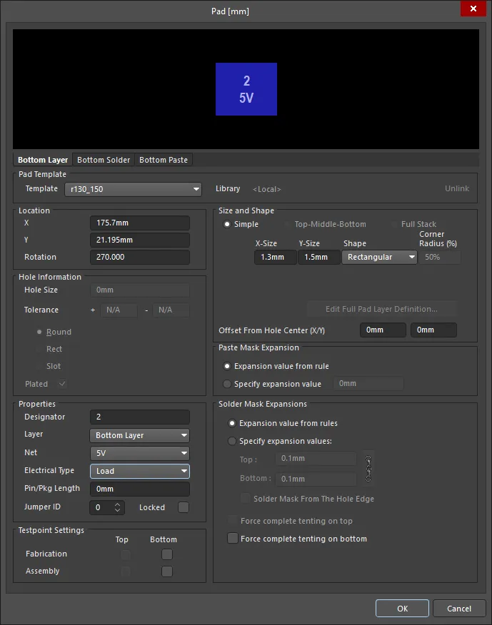
The Pad dialog
To toggle the units of measurement used in the open dialog between metric (mm) and imperial (mil), press the Ctrl+Q shortcut.
Pad Template
-
Template - select a Pad template from the dropdown.
-
Library - displays to which library the Pad template is linked and includes the option to unlink the template from that library.
Location
Values can be defined in either mm or mil units. When entering a value in units other than the current units, add the mm or mil suffix to the value.
-
X - the current X position of the center of the pad, relative to the current origin. Edit the value to change the position of the pad relative to the origin.
-
Y - the current Y position of the center of the pad, relative to the current origin. Edit the value to change the position of the pad relative to the origin.
-
Rotation - the current pad rotation in degrees. Edit to change the rotation of the pad. Minimum angular resolution is 0.001°.
Hole Information
-
Hole Size - the current hole size for the pad. The value specifies the diameter of the hole (in mils or mm) to be drilled in the pad during fabrication. For a single-layer pad (such as an SMD pad or edge connector), this is automatically set to zero. The hole size can be set from 0 to 1000mil and can be set larger than the pad area to define copper free mechanical holes. Edit the value in this field to change the pad hole size. Values can be entered in either mm or mil units.
-
Tolerance - Setting the hole tolerance attribute can help determine the fits and limits of your board. Specify the minimum (-) and maximum (+) hole tolerance for the design.
Choose one of the following options to specify the shape of the hole:
-
Round - specifies a round hole shape (default) for the pad.
-
Square - specifies a square (punched) hole shape for the pad.
-
Slot - specifies a round ended slotted hole shape for the pad.
-
Plated - this option determines whether or not the pad has a plated hole. If both plated and non-plated pads exist in a design, the non-plated holes will be set to use different tools from the plated holes in the NC drill files.
Separate drill files (NC Drill Excellon format 2) are generated for each hole kind (Round, Square and Slot) as well as for plated and non-plated holes (as defined by the Plated checkbox). This means there can be up to six different drill files generated.
Properties
-
Designator - the current pad designator. If the pad is part of a component, the designator is usually set to the corresponding component pin number. The designator can be up to 20 characters in length and cannot include any spaces. Free pads can include a designator or the field can be left empty. If the designator begins or ends with a number, the number will auto-increment when placing a series of pads sequentially. Edit the value in this field to change the pad designator. Note that multiple pads within the same component footprint can share the same designator, if required.
-
Layer - the layer the pad is currently assigned to. Pads can be assigned to any available layer, Set the Layer to
Multi-Layer to define a pad shape on all signal layers.
-
Net - the net to which the pad is currently assigned. Change the net assignment by clicking in the field and choosing a net from the drop-down list. Select No Net to specify that the pad is not connected to any net. The Net property is used by the Design Rule Checker to determine if a PCB object is legally placed.
-
Electrical Type - this field displays the current electrical status of the pad. This status is only relevant for component pads, and sets the transmission line characteristics for these pads. Pads can be designated as a Load, Source or Terminator. The Source and Terminator settings are used when a net requires one of the Daisy chain routing topologies. Click the field to change the electrical type from the drop-down list.
-
Pin/Pkg Length - the Pin Package Length is automatically included in the Signal Length calculations that are displayed in the PCB panel. Set the PCB panel to Nets mode to examine (or edit) the value of the Pin/Pkg Length for the pins in the chosen net.
-
Jumper ID - set this to a non-zero value (range of 1-1000) to indicate that this pad is part of a jumper component footprint. Jumper components can be used on a single-sided PCB when there will be a wire link that physically connects the pads together rather than using tracks to create the connection. The Jumper ID value tells the software which pads to treat as 'connected'. A jumper connection can only be created between the pads within the same component footprint; they must have the same Jumper ID value and must also be assigned the same net. The component must also have its Type set to Jumper. When these conditions are met, a jumper connection is shown as a curved connection line in the PCB Editor.
-
Locked - enable to protect the pad from being edited graphically. Lock a pad whose position or size is critical. If you try to edit a primitive that is locked, you will be informed that the primitive is locked and asked if you wish to proceed with the action. If this option is unchecked, the primitive can be freely edited without confirmation. Note that the Locked checkbox has no effect on a pad that belongs to a component. If the component is not locked, the pads will move when the component is moved. In this situation, lock the component to prevent accidental movement.
Testpoint Settings
Use this region to define this pad as a testpoint for Fabrication and/or Assembly testpoint file generation. A testpoint is a location where a test probe can make contact with the PCB to check for correct function of the board. Any pad or via can be nominated as a testpoint by enabling the required Testpoint Type and Layer checkbox(es). When this is done, the pad or via is automatically locked, and if the pad belongs to a component, the component is also locked. The pad/via/component can be temporarily unlocked if it needs to be moved. Note that disabling the testpoint settings does not automatically unlock the pad/via/component, this must be done manually.
-
Top - enable this option for this pad to be defined as a top layer testpoint.
-
Bottom - enable this option for this pad to be defined as a bottom layer testpoint.
Size and Shape
The copper area (land area) of the pad is defined by the X and Y size and the Shape setting.
-
Simple - a simple pad is one whose size and shape is identical on all layers.
-
Top-Middle-Bottom - a Top-Middle-Bottom layered pad supports defining different X and Y sizes and shape for the top layer, for all mid signal layers, and for the Bottom layer, separately.
-
X-Size - the current X (horizontal) size of the pad. Enter a value from 1 to 10000mil. The X and Y size can be set independently to define asymmetric pad shapes.
-
Y-Size - the current Y (vertical) size of the pad. Enter a value from 1 to 10000mil. The X and Y size can be set independently to define asymmetric pad shapes.
-
Shape - the basic pad shape. Basic pad shapes include
Round, Rectangular, Octagonal, or Rounded Rectangle. The basic shape can be manipulated by changing the X and Y size settings to produce an asymmetrical pad shape.
-
Corner Radius - this option is available when the Shape is set to
Rounded Rectangle. The value is a percentage of half of the shortest side of the pad, therefore, a value of 0% corresponds to a rectangular pad and 100% to a circular pad.
-
Offset From Hole Center (X/Y) - enter a value to offset the pad land area from the center of the pad hole by this amount.
-
Full Stack - different hole sizes and diameters can be edited at each layer (including all signal layers and planes).
-
Edit Full Pad Layer Definitions - click to open the Pad Layer Editor dialog that provides controls related to pad/via settings for each layer, including pad shape, size, and X/Y location. Full Stack must be selected to access this button.
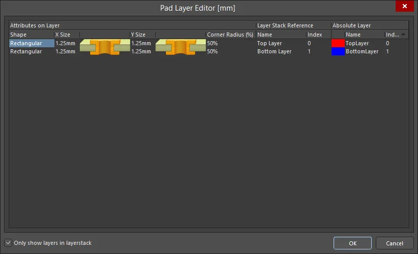
The Pad Layer Editor dialog
Options and Controls of the Pad Layer Editor Dialog
-
Main Grid - A pad stack is a collection of pad information about the pad shape and size relative to a layer of this stack. Click on one of the attributes on this grid to edit the values for the current layer of the stack. The layers of a pad stack are derived from the Layer Stack Manager (Design » Layer Stack Manager).
-
Attributes on Layer
-
Shape - choose a pad shape from drop-down list: Round, Rectangular, Octagonal, or Rounded Rectangle.
-
X Size - click to specify the X size of the pad.
-
Y Size - click to specify the Y size of the pad.
-
Corner Radius (%) - click to specify the corner radius of the pad; this field is editable only for Rounded Rectangle.
-
Layer Stack Reference
-
Name - the layer referenced by the pad layer.
-
Index - the relative index of the layer.
-
Absolute Layer
-
Name - name of the layer, which is defined by default.
-
Index - absolute index of the pad among all layers (including hidden layers).
-
Only show layers in layerstack - enable this option to display only the layers (derived from the Layer Stack Manager) in the Layer Stack. Check the Layer Stack Manager (Design » Layer Stack Manager) to see which layers are used. If this option is disabled, all the available PCB layers are displayed.
Paste Mask Expansion
An opening in the paste mask is automatically created by the software that is the same shape as the pad. This opening can be larger (a positive expansion value) or smaller (a negative expansion value) than the pad itself as defined by this setting. Typically, paste mask openings are smaller than the pad, but there are exceptions to this.
-
Expansion value from rules - when this option is enabled, the paste mask expansion for this pad is defined by the applicable Paste Mask Expansion design rule.
-
Specify expansion value - Enable this option to override the rule and specify the paste mask expansion value for this pad.
Solder Mask Expansions
An opening in the solder mask is automatically created by the software that is the same shape as the pad. This opening can be larger (a positive expansion value) or smaller (a negative expansion value) than the pad itself as defined by this setting. Typically, solder mask openings are larger than the pad, but there are exceptions to this.
-
Expansion value from rules - when this option is enabled, the solder mask expansion for this pad is defined by the applicable Solder Mask Expansion design rule.
-
Specify expansion value - enable this option to override the rule and specify the solder mask expansion values for this pad.
-
Solder Mask From The Hole Edge - if the expansion value is being specified in this dialog, you also can enable this option to define the solder mask expansion from the edge of the hole instead of the edge of the pad.
-
Force complete tenting on top - the term tenting means to close off. If this option is enabled, the settings in the applicable solder mask expansion design rule will be overridden, resulting in no opening in the solder mask on the top solder mask layer for this pad. When this option is enabled, the Expansion value from rules and the Specify expansion value options are ignored.
-
Force complete tenting on bottom - the term tenting means to close off. If this option is enabled, the settings in the applicable solder mask expansion design rule will be overridden, resulting in no opening in the solder mask on the bottom solder mask layer for this pad. When this option is enabled, the Expansion value from rules and the Specify expansion value options are ignored.
Paste and Solder masks are shown in the negative, i.e., when you see an object on one of those layers, it is actually a hole or opening in that layer.
Reporting on Nets
To generate a Netlist Status report from the active PCB document, choose the Reports » Netlist Status command from the main menus. This report provides detailed information regarding the netlist for the routed board. It lists all nets and for each net, indicates the layers used for routing and the total physical routed track length. After launching the command, a report - Net Status - <PCBDocumentName>.html - is generated and opened as the active document. Each net is listed; click a net name to highlight that net on the PCB document. The physically-routed track length data is initially displayed in the measurement units specified for the board design itself. Use the Units field in the report to quickly change between imperial and metric units as required.
-
The report is also generated in .txt format. Both report formats are stored in the folder specified by the Output Path entry on the Options tab of the Options for Project dialog. Only the HTML-formatted report is added to the parent project in the Projects panel and can be found in the Generated\Documents sub-folder.
-
The report includes the Routed Length, which includes the vertical distance traversed through the vias in that net. Note that the Routed Length calculator does not attempt to resolve overlapping track segments or routing wiggles inside pads, so may not be accurate. For a more accurate length use the Signal Length, which can be displayed in the Nets mode of the PCB panel. The PCB panel also supports creating a report, right-click in the list of nets in the panel to configure the required columns, then right-click and select Reports to open the Report Preview dialog, where you can export the report in a variety of formats.