The PDN Analyzer (PDNA) application is relatively straightforward to use, and basically involves setting up the PI-DC simulation net parameters, running the simulation and then interpreting the results. The data used in a PDN Analyzer power net simulation is drawn directly from the currently loaded PCB design project, which can be iteratively edited to improve the power integrity of the supply paths and the PDN simulation then re-run to test the results.
This demonstration guide to working with the PDN Analyzer uses two reference designs available from Altium:
Additionally, the PDN Analyzer installation includes the SpiritLevel PCB project with a number of analysis configuration file examples. Access and then unzip the project and samples via the PDNA File » Explore Samples menu option.
This guide information assumes that the PDN Analyzer is available in your Altium Designer instance, and that you have a base understanding of the PI-DC (DC Power Integrity) principles used.
See the PDN Analyzer page for information on accessing the PDN Analyzer functionality, and also the basics of PI-DC simulation.
PDN Analyzer Interface
The PDN Analyzer extension's interface is invoked as an Altium Designer non-modal window, which can be positioned in any convenient location in the workspace or on another screen, if available. To open the main PDN Analyzer window, open a project's schematic or PCB document and select the application from the Tools menu (Tools » PDN Analyzer).
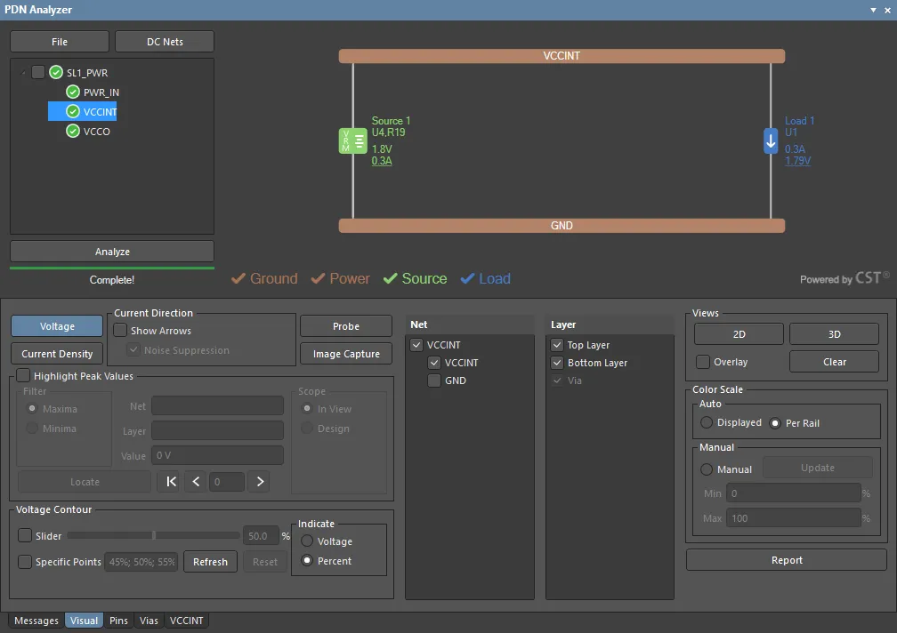 The PDN Analyzer GUI with a single power network selected. The display and results configurations are available in the lower panel section.
The PDNA window GUI is arranged with an upper section devoted to file/net control and an interactive representation of the currently selected power network(s), while the lower panel section provides access to the analysis options, display settings and results data. Multiple, interconnected nets are supported by PDNA version 2, which allows the DC power integrity of an entire PCB design to be analyzed as a hierarchical structure or as individual power nets.
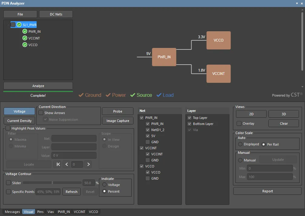 The PDN Analyzer GUI with the complete power net hierarchy selected. The display of the included networks and layers is controlled in the lower panel section.
The PDN interface also offers a compact screen mode (File » Compact Layout) that does not include the lower panel section, which is ideal for horizontal/vertical docking in the main Altium Designer screen. To enable screen docking for the compact or standard screen modes, right click in the PDNA interface title bar, select Allow Dock from the context menu and choose the Horizontally or Vertically option.
See the collapsible section below for details on the user interface of the PDN Analyzer panel.
PDN Analyzer Panel
Layout Modes
The dockable PDN Analyzer panel is best used in conjunction with the software's PCB Editor so the visual results of analysis run may be seen immediately in the design's copper layout. In its floating (undocked) mode the panel might be moved to a second monitor to maintain visual access to the PCB Editor, or the panel may be vertically/horizontally docked in the main design screen to share real estate with the PCB Editor.
For the latter case, the panel offers a compact interface mode that moves its main configuration pane to a separate tab option (Config). To switch to this mode, select the Compact Layout option from the panel's  button drop down menu in the configuration pane/tab.
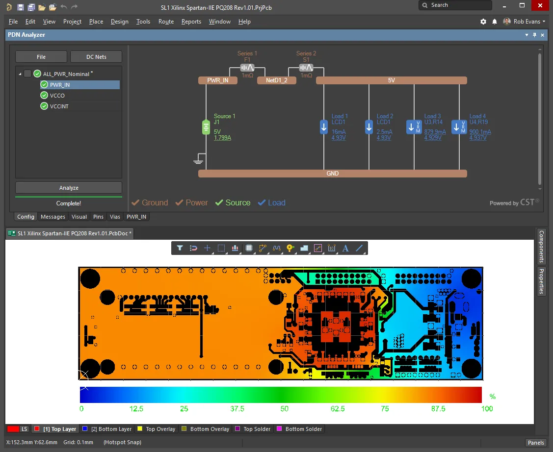 In Compact Layout mode the Configuration pane changes to tab access, which preserves screen space for the PCB Editor.
Configuration
The Configuration pane (or Config tab) is devoted to simulation network control and presents an interactive graphic representation of the currently selected power network(s).
Simulation and network management
The section on the left of the Configuration pane/tab is used for simulation file management, and provides a hierarchical view of the simulation's loaded power networks. The complete network structure or individual power networks may be selected. The section's options include:
-
The
 drop down menu.
-
New Simulation – start a new PDN simulation, based on a single power/ground network.
-
Open – open a previously saved or example simulation configuration file (
*.pdna).
-
Save – save the active simulation configuration to disk as the current name.
-
Save As – save the active simulation configuration to disk as the desired name.
-
Explore – open a Windows file browser in the location of the active simulation.
-
Explore Samples – open a Windows file browser in the location of the installation's example project (stored as a zip archive) – unzip this project to a convenient location. Note that the project also includes a set of example PDN Analyzer configuration files, where each is set to a specific copper temperature; 25°C (nominal), 100°C, 175°C.
-
Compact layout – the alternative screen mode outlined above.
-
Right click options – accessed by right clicking on the top level simulation name.
-
Import (1.x) – load a simulation configuration saved from the previous
1.xx version of the PDN Analyzer (*.pidc_config).
-
New Network – create a new base-level network within current simulation configuration.
-
Remove – unload the selected simulation.
-
Delete – remove the selected network from the simulation (available as a right click option on the name of an individual network).
-
Clear Results – reset the power network analysis results, including those cached from a previous simulation run.
-
Revert – restore the last simulation analysis results and its corresponding configuration.
-
Save – save the active simulation configuration to disk as the current name (
*.pdna).
-
Save As – save the active simulation configuration to disk as the desired name.
-
Copy – clone the selected network simulation.
-
Explore – open the
/PDNAnalyzer_Output folder for the current simulation in a Windows file browser. Note that this includes a fully detailed event log file for the most recently run simulation (PDNAnalyzer.log).
-
Settings – opens the Settings dialog for the current simulation configuration. The settings can be exported/imported (
*.pdna.settings) and reset to their defaults.
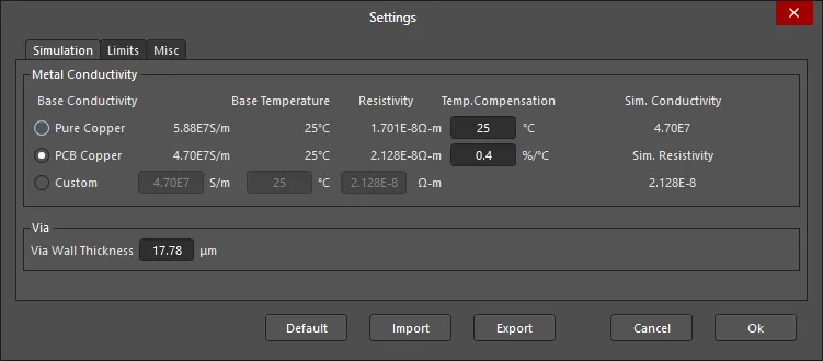
The dialog includes the:
-
Simulation tab – specify the Metal Conductivity settings for the physical board copper and the weight (wall thickness) of the layer connection Vias.
-
Limits tab – specify the maximum current density limits detected by the simulation for both copper layers and Vias of two sizes.
-
Misc tab – set simulation parameters such as the applied current density units and data smoothing (Noise Filtering), and voltage offset scheme used to establish the design's zero voltage reference.
-
The
 button, which opens the PDN Analyzer DC Net Identification dialog – also opened when the PDN Analyzer is first invoked. The system will attempt to automatically detect suitable DC power nets within the current PCB design.
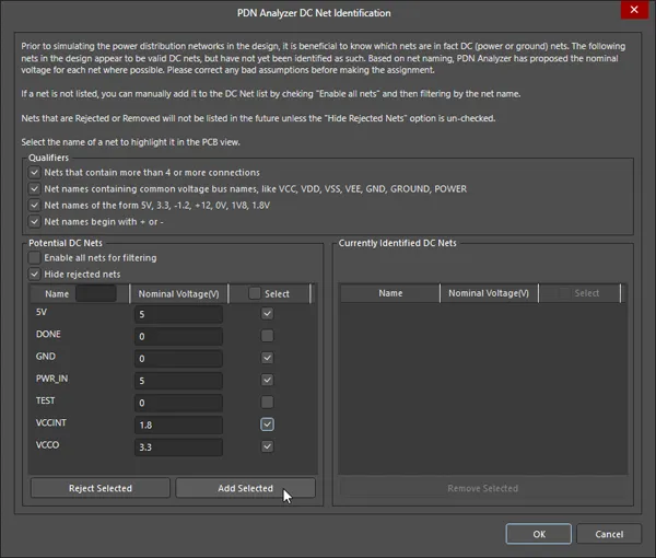
Use the dialog options to help correctly identify the DC nets and their nominal voltage levels.
-
Qualifiers – deselect qualifier filters if necessary to correctly identify the design's DC nets. The filters are based on number of connection and common power network nomenclature.
-
Potential DC Nets – a tabular list of the identified power net in the design. Use the Enable all and/or Hide rejected options to populate the list as needed for your DC power analysis.
-
Name – the net name as extracted from the board design's net data. Use the associated search field to filter the listing by an entered key word.
-
Nominal Voltage – enter a suitable voltage for power nets as basic source data for the analysis.
-
Select – use the checkboxes to nominate which nets would like to be registered (identified) by the PDN simulation.
-
Reject/Add Selected – use the
 and
and  buttons to manage which nets are populated into the Currently Identified DC Nets listing.
-
Currently Identified DC Nets – a tabular list of power nets that will be available to the PDN simulation, as populated from the Potential DC Nets listing.
-
Select – use the checkboxes to select nets that will be removed (moved from the identified nets list back to the potential nets list) by the
 button.
Click on a net entry to cross probe to that net in the PCB Editor.
-
The
 button, which invokes the power network simulation and analysis routines. This button is enabled when the power network and its related data is fully configured, as indicated by tick icons associated with the Ground, Power, Source and Load labels in the power network diagram graphic.
Power Network Graphic
The main body of the Configuration pane provides an interactive graphic representation of the power network structure selected in the simulation's network tree (on the left). When the top level simulation name is selected, the graphic shows the overall connectivity of sub power networks – double click on a sub network graphic element to open that sub network. The interactive graphic also is used to construct a power network from the PCB design's net data and connectivity by using its right-click options, or by double-clicking on graphic elements.
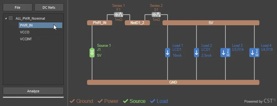
Hover the cursor over an active element (Source, Load, series device, etc) to see a summary of its properties, connectivity and if applicable, analysis results.
► See Example 1, Example 2 and Example 3 below for detailed information on creating various types of power networks.
Right click on the configuration graphic or one of its elements to access the following options:
-
New Network – create a new base-level network (power and ground nets) within current simulation.
-
Edit Net – specify a power network's settings in the Choose Net dialog (also available by double-clicking on a network element). The dialog includes a selectable list of nets available to the simulation (as defined in the PDN Analyzer Net Identification dialog, opened from the
 button) and several filter options that can be used to constrain the listing.
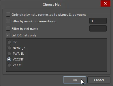
-
Extend Net – use to add another net to the selected net via a series element, which will be inserted automatically. The additional net is selected in the Choose Net dialog, while the inserted series device is configured by double clicking on its element to access the Device Properties dialog. See Extending Networks Through Series Elements for more information.
-
Add Source – add a Voltage or Voltage Regulator Model (VRM) source device between a specified power/ground net pair via the Device Properties dialog. The dialog also is available by double-clicking on an existing Source element. See Including Voltage Regulator Models for more information on working with VRMs.
-
Add Load – add a Resistor, current sink or Voltage Regulator Model (VRM) load device between a specified power/ground net pair via the Device Properties dialog. The dialog also is available by double-clicking on an existing Load element.
-
Delete – remove the power net from the simulation. Note that a network must include one power net and one ground net as a minimum.
-
Settings – open the Settings dialog, as outlined above.
The Device Properties dialog, used when adding or editing an existing device element (Load, Source, etc) provides settings to specify the device type, connectivity and parameters.
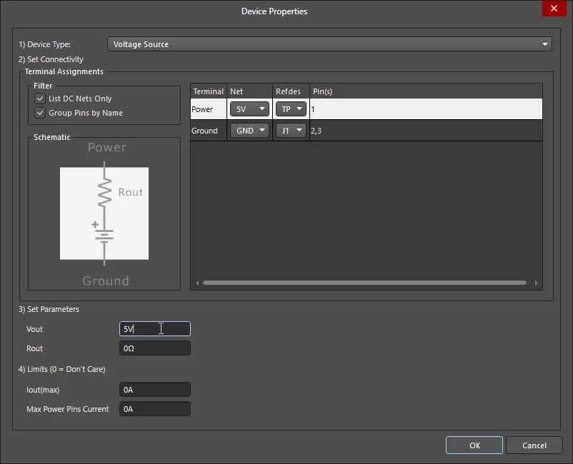
The dialogs's available settings options will depend on the function of the device element being placed or edited, but are generally as follows:
-
Device Type – use the drop down menu to select type of device, where the available options are determined by the element type (Source, Load, etc).
-
Set Connectivity – use the listing's Net and Refdes dropdown options to choose the device's Terminal connections from the available nets and nodes, where the Terminals are as indicated in the Schematic simulation model graphic. The net connection Pins are automatically assigned based on the specified node's net connectivity.
-
Filter – use List DC Nets Only option to constrain the available Net options, and the Group Pins by Name option to combine interconnected device pins. When the latter is disabled, individual pins can be selected/deselected as required using the Select checkboxes exposed by clicking in the Pins field. See the LCD example in Working with Loads for more information.
-
Set Parameters – the available parameter options will depend on the type of device being placed (or edited), but generally define its base properties such as the output voltage and internal resistance of a Voltage Source, the load current of a Current sink, or the resistance value of a Resistor load.
-
Limits – the device's Voltage, Current or Power limitations that will trigger a Violation when the simulation is run. A violation is indicated by a dashed red border around the graphic of the offending element and a red icon associated with the network name: see Current Density Limit Violations or Other Violations for examples.
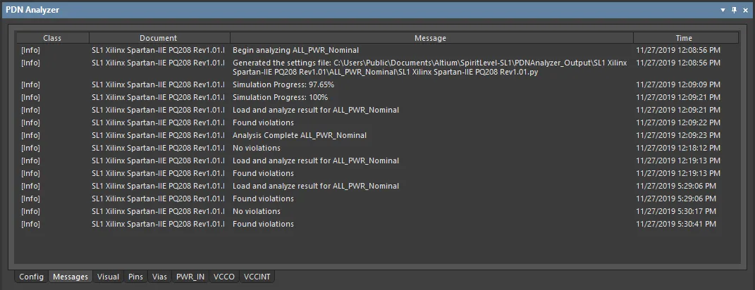
Messages tab
The Messages tab includes a sequential listing of simulation events for the most recently run PDN analysis, including any Violations that were encountered. In the situation of a failed simulation run, the list will include an event entry summarizing the issue. For more information on a simulation run, see the PDN_Analyser.log file available via the configuration Explore option.
Visual tab
The PDN Analyzer interface's Visual tab provides a high level of control over how the power network analysis data is displayed in the PCB Editor. It allows you to specify what type of information is included in PCB layout rendering, the scaling of the results data, how and if points of interest are highlighted, and what information is exported. The rendered layout in the PCB Editor applies to the power network that is currently selected in the PDN Analyzer's Configuration network hierarchy.
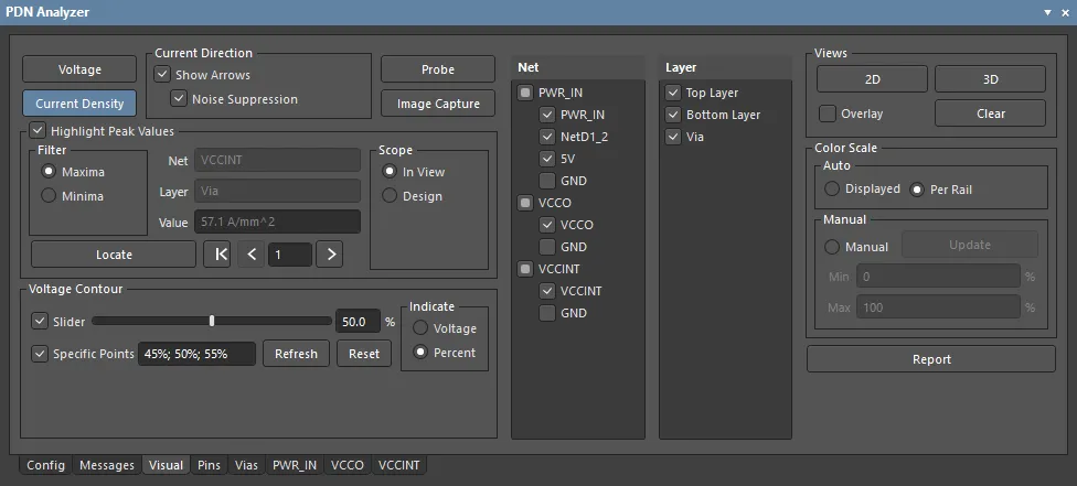
Use the Visual tab's default settings as a starting point for setting up the PCB layout display. These are set to show the color-graduated voltage profile across all power rail nets in 2D mode – deselect the Overlay option to see the pure analysis results. Setting changes made in the Visual tab are immediately reflected in the PCB rendering.
The Visual tab options include:
-
Voltage – select the
 button to display the voltage profile across all enabled nets, scaled in Volts or as an overall percentage span (see Color Scale).
-
Current Density – select the
 button to display the current density profile across all enabled nets, scaled in Amps per area or as an overall percentage span (see Color Scale).
-
Current Direction – check the Show Arrows option to overlay current direction/distribution indicator arrows on the rendered PCB layout. Select the Noise Suppression option to apply data smoothing for a less cluttered visual result.
-
Probe – select the
 button to open the Probe dialog, where two data locations in the rendered layout can be interactively selected and their numerical values compared. See Data Probe for more information.
-
Image Capture – select the
 button to open the Manage Image Capture dialog, where the current PCB rendering can be captured and saved. The images are stored in the project simulation's
 /HTMLReport/ImagesCache folder for later inclusion in a Report. See Analysis Report for more information.
-
Peak Values – select the Highlight Peak Values option to visually mark and highlight the maximum or minimum (as per the Filter options) Value in the currently selected nets and layers. Use the Scope options to specify the detection area, the Locate button visually highlight the peak value point, and the data point arrows (

 ) to step though the adjoining sequence of values. See Locating Power Integrity issues for example information.
-
Voltage Contour – select the Slider option to enable a dashed line overlay which represents the voltage level at that contour line. The detected level is that set by the slider position, and is a voltage or percent value as determined by the associated Indicate options. Select the Specific Points option to enable voltage contour lines at each on the indicated percentage points. Click
 to set the Specific Point values to their defaults, and the
  button to update/highlight all enabled voltage contour lines. See Voltage Contour for more information.
-
Net – select the Nets you wish to display in the rendered PCB analysis results. The nets are grouped by available power networks.
-
Layer – select the board Layers you wish to display in the rendered PCB analysis results. Note that Vias are available for selection when in 3D view mode.
-
Views – use the
 and
and  buttons to change the rendered display between the PCB Editor's 2D/3D modes, the Overlay option to enable/disable the editor's standard PCB display view, and the
  button to revert the rendered display to the standard view. See Display Control and Options for more information.
-
Color Scale – set the Auto options to show the rendered color gradient as an overall percentage range (Per Rail) or as a gradient that corresponds to the complete voltage span data (Displayed). The latter is best used when a single net is being displayed. Select the Manual mode to override the displayed range to the voltage values entered in the Min and Max fields. See Visual Rendering in the PCB Editor for more information.
-
Report – click the
 button to configure and generate an HTML-based PDN Analysis report via the HTML Report dialog. See Analysis Report for more information.
Pins tab
The Pins tab presents a list of all component pins in the design connected to configured power networks. Each component pin entry includes its number, connected net, and the associated Voltage and Current value results from the last simulation run. Click on a column header to order the list by that name, and click again to reverse the order.
Double click on an entry to cross probe to that pin in the PCB Editor. If the pin (pad) connection cannot be seen in the rendered view, ensure that the Layer and power Net it is connected to are enabled in the Configuration pane/tab.
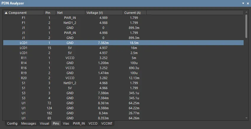 The Pins tab listing ordered by Component reference and – hover the cursor over the image – ordered by pin Current.
Vias tab
The Vias tab presents a list of all PCB vias in the design connected to configured power networks. Each via entry includes its connected net, location co-ordinates, layer pair, and the associated end-to-end Voltage, Current and Current Density value results from the last simulation run. Click on a column header to order the list by that name, and click again to reverse the order.
Double click on an entry to cross probe to that via in the PCB Editor. If the via cannot be seen in the rendered view, ensure that Via is checked in the Layer list (available in 3D view) and its connected power Net is enabled in the Configuration pane/tab.
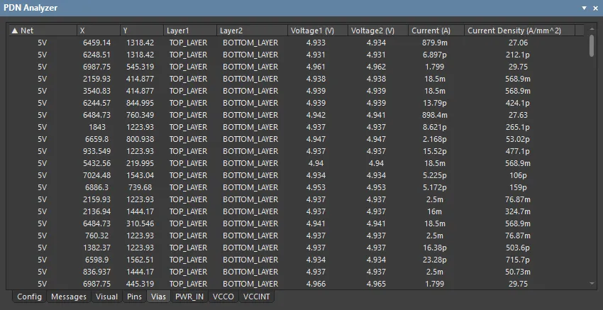 The Vias tab listing ordered by Net connection and – hover the cursor over the image – ordered by Current Density.
Power Network tabs
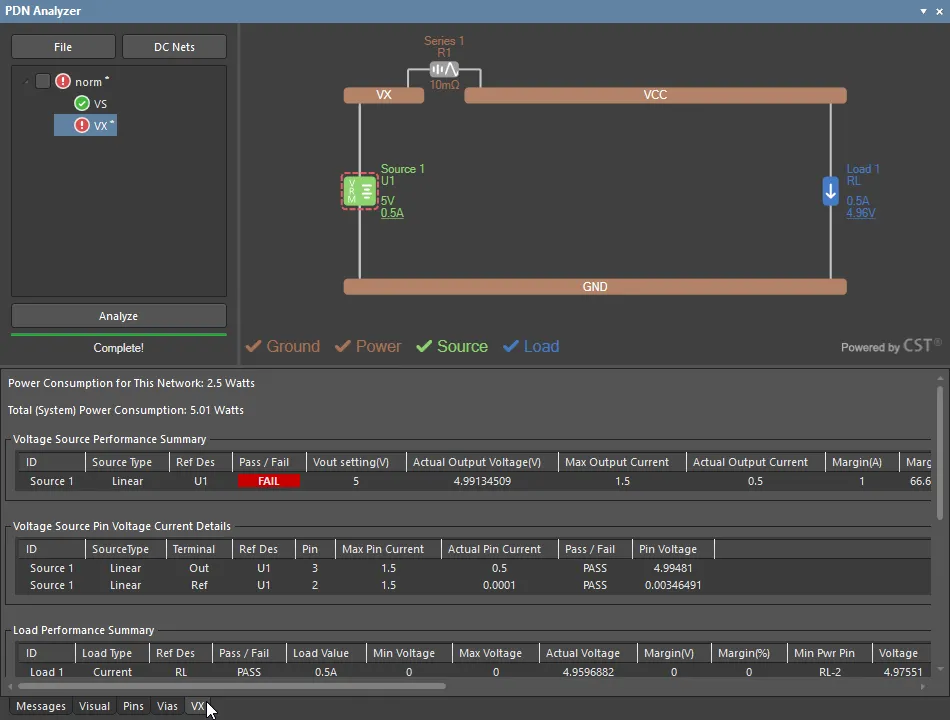
A tab view is available for each available power network within the simulation configuration – the network tabs that are visible is determined by the power network selection in the Configuration pane/tab. Labeled as the network name, the power network tab provides a comprehensive listing of grouped simulation results and calculated data that applies to that power network. A network power consumption summary is also included.
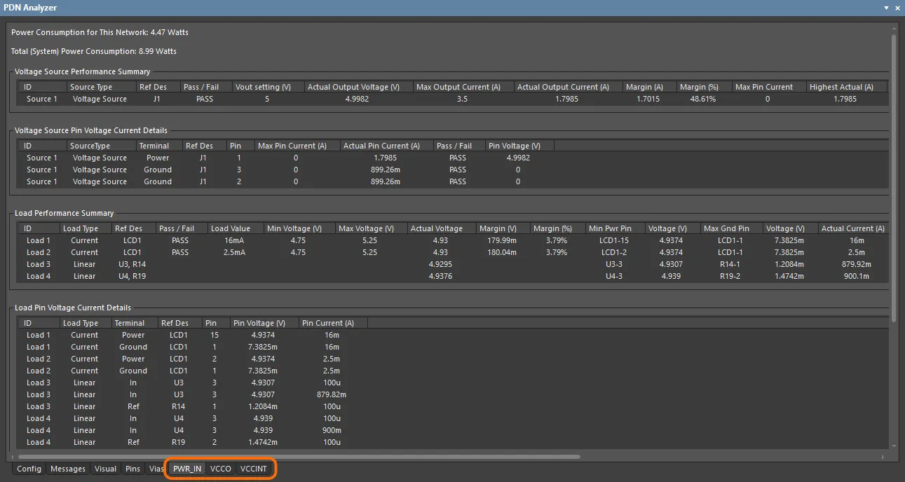
The data groups in the listing apply to devices within the power network (sources, loads, and series elements), where a Performance Summary and a Pin Voltage/Current Details data entry is included for each device. Along with details about the device, the data groups present key voltage and current values, and in the case of the Performance summary, calculated safety margins that relate to the device limits as specified in the Device Properties dialog.
DC Net Identification
When the PDN Analyzer is initially opened for a PCB design, it will attempt to identify all DC power networks from the design's net data based on common power network nomenclature. If all potential power nets have not been identified, deselect appropriate Qualifiers filter options, or to see all nets, select the Enable all nets for filtering option.
Use the Select check boxes to choose which power nets will be available to the PDNA analyzer, and enter suitable voltage levels in their matching Nominal Voltage fields. Click the Add Selected button to populate the Currently Identified DC Nets list and confirm these nets as identified power networks.
Note that double clicking on a listed net entry in the dialog will cross probe to that net in the PCB layout.

Further nets can be identified and applied during the PDN analysis setup by selecting the DC Nets button in the analyzer's GUI.
The below analysis examples are included to demonstrate the major capabilities and features of the PDN Analyzer. Each example only shows one of many possible parameter configurations that could be used to assess the network's power integrity in differing ways, depending on the focus of interest. Note that an analysis that has completed successfully may be saved as a PDNA configuration file (*.pdna) and reloaded at any time – File » Save As and File » Open (by default in the project's PDNAnalyzer_Config folder)
Example 1
This example demonstrates the basics of setting up a power integrity simulation with a simple power net and its current loads. It is configured to assess the 5V supply rail distribution and its ground return path in the SpiritLevel-SL1 reference project, when loaded with the design’s LCD display. In this case, the 5V supply rail is considered as a simple voltage source, and its connected networks (such as via switch S1) are not included.
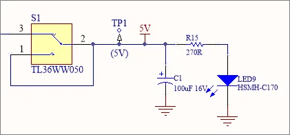
The preliminary conditions for this PDN simulation example are:
-
the Spirit Level PCB project is open in Altium Designer
-
the PDN Analyzer application is active (Tools » PDN Analyzer)
-
the PCB design's DC Nets have been identified in the PDN Analyzer DC Net Identification dialog, as outlined above.
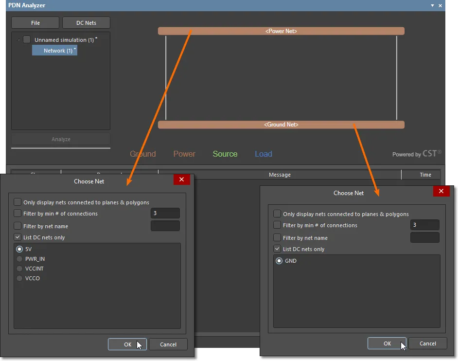
Begin the analysis process by specifying the power and ground nets. Double click on the <Power Net> and <Ground Net> elements in the GUI network graphic to open the Choose Net dialog, which will offer the choice of power nets that have been identified.
If necessary, use the dialog's qualifier/filter options to restrict or expand the listed nets, or return to the main screen and select the  button re-identify the DC power nets.
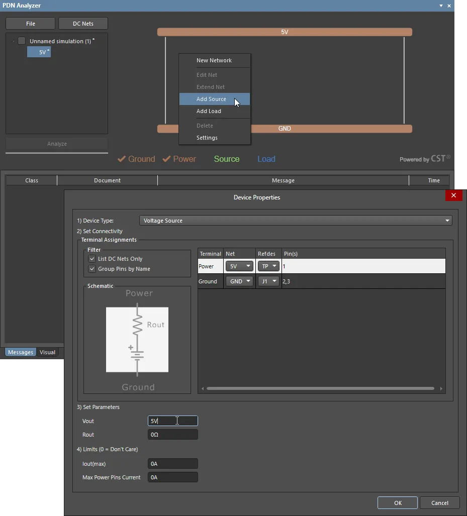
A Source or Load element can now be added between the specified power and ground networks – note that the Ground and Power status indicators change to a checked state (✔). Right click in the network graphic workspace and select Add Source (or Add Load) from the context menu to open the Device Properties dialog. The steps, as indicated in the dialog, are as follows:
-
To add a power Source for the network, in this case a simple voltage source, select the Voltage Source option from the dialog's Device Type drop down menu.
-
In the source connectivity listing, the PDNA will attempt to choose the correct net connection options based on the power network parameters – this is between the
5V and GND nets. Use the Refdes drop down menu options to specify the component connection points of the source voltage. In this example the source voltage point is nominated as TP1, and its ground return as the design's DC input socket J1 (pins 2 and 3).
-
In the lower section of the dialog, the source parameters specify the attributes of the voltage source simulation model. Here, the source voltage (Vout) is set to
5V and the model's internal resistance (Rout) left at the default 0Ω setting.
-
Finally, the maximum source current and pin current (for sources with multiple output pins) are left at the default settings (
0A: Don't Care). When the Limits are set to specific current values, the PDN analysis will flag a Violation if the simulation results exceed those values.
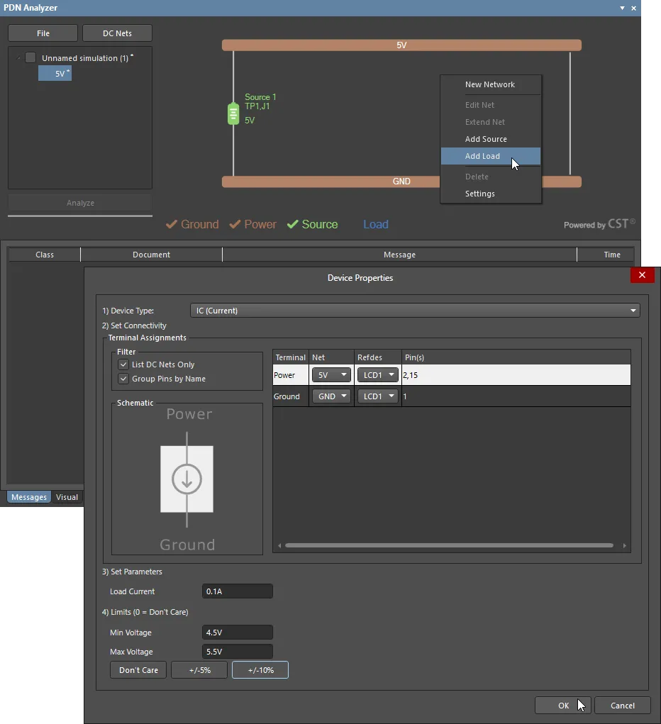
Using the same approach as when adding a Source to the network, add a Load and specify its parameters in the Device Properties dialog.
In this case a current sink load (Device Type: IC (Current)) is added to represent the current drawn from the 5V rail by the design's LCD component. Note that a purely resistive load option is also available, by choosing Resistor as the Device Type.
Set the load connection as LCD1 and specify the Load Current it will draw from the 5V supply – note that unit prefixes (for example, 500m to represent 0.5A) are supported. While the voltage Limits settings are optional, these have been set to +/-10% (using the related button), which will trigger a simulation violation if the voltage at the load itself drops below 4.5V (or is above 5.5V).
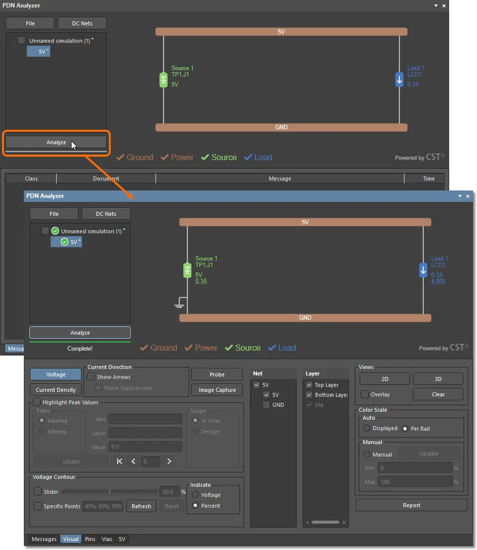
With the power network defined and all parameters specified (all network elements have an associated ✔ status), the PDN analysis can be run by selecting the  button. The progress of the simulation is shown under the Messages tab as a stream of events, which will also indicate the cause of a simulation failure if the process is unable to complete.
When an analysis is run, the current simulation configuration – the specified nets, sources/loads etc, and their related parameters – is stored along with the analysis results data (File » Explore; see PDNAnalyzer_Ouput folder). This configuration setup can be restored at any time for the current simulation by right-clicking on the simulation name and choosing Revert from the context menu.
The immediate results of the PDN analysis can be seen in the network graphic, which will include the calculated load/source voltage and current levels (where applicable), and the highlighting of any sections of the network that have caused a parameter Violation. Note that the Visual tab is now focused and active.
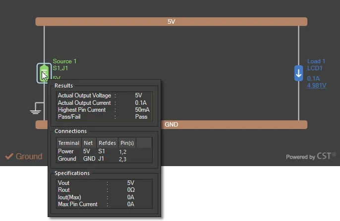
Hover the cursor over any element in the network (Load, Source or Series Element) to see additional information such as its specified parameters and analysis results.
Visual Rendering in the PCB Editor
The results of simulation can now be viewed graphically in the Altium Designer PCB editor, under the control of the settings available in the PDNA's Visual tab. Set the visual options to display Voltage for both Layers (Top and Bottom) of the 5V Net – the initial default display settings. The analyzer results are rendered in the PCB Editor to replace the existing PCB graphics overlay.
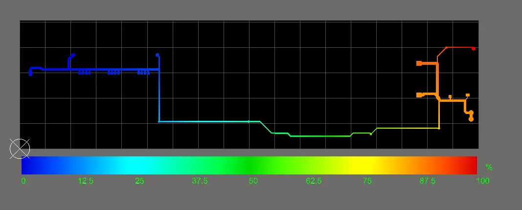
The view of the selected net path voltage drop, in this case from the 5V source at TP1 to the LCD1 component, is rendered with a color gradient that corresponds to the Voltage scale presented at the bottom of the view. This is shown as a voltage percentage (the Per Rail option under Color Scale), or as a literal voltage span (the Displayed option).
In the below image, the color transition through the board's network path represents its overall voltage drop, where the minimum level (0%: blue) due to IR losses is at the LCD1 component, and the maximum level (100%: red) is at the specified voltage source point (TP1).
To display the corresponding current analysis for the network, select the Visual tab's Current Density option. Here, the color levels in the board's network path relate to the percentage of the current density variation, where 100% (red) indicates the maximum calculated current density in the network path layout, and 0% (blue) is the minimum – most likely 0A/mm2.
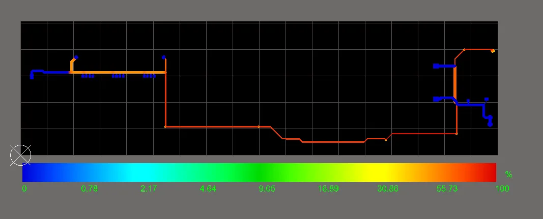
Note that while the alternative voltage/current scale option (Displayed) is a more intuitive scale style for the display of single networks, it provides limited useful information for the simultaneous display of multiple voltage networks – such as 5V and GND in this example, or where several power supply networks in a design have been analyzed.
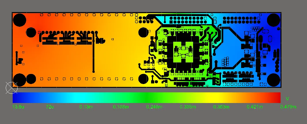
To display and analyze the power integrity results in the example's GND return path, deselect the 5V network option in the Net list under the PDNA's Visual tab and then select GND network. The ground return path is via both the design's Top and Bottom layers, which can be displayed individually in the PCB Editor by selecting each entry in the PDNA's Layer list.
The below image shows the Voltage display for the Bottom layer of the GND net, with the Color Scale scale set to Displayed. The highest level of voltage drop (red: approximately 0.5mV) is located at the LCD's GND pin, while the least voltage drop (blue: approximately 0V) is at the voltage source return point (J1).
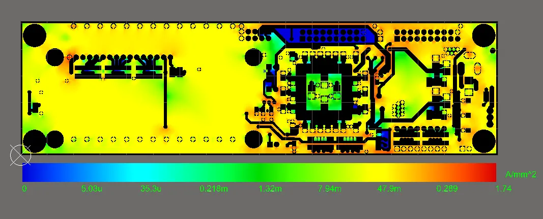
Switching to the PDNA's Current Density option shows the maximum current 'hotspots' in red. The maximum current density level itself (1.74 A/mm2) very low and well within acceptable limits.
Display Control and Options
The PDN Analyzer offers several interactive display options that determine how the analysis results are graphically represented in the Altium Designer PCB Editor. Along with the options for the display Color Scale, the graphics can be switched between 2D and 3D rendering, where the latter provides a valuable insight into the analysis results through Vias and between layers.
An option is also provided to Clear the analysis results from the editor display, which automatically reverts to the graphic rendering to the standard board layout. By contrast, the view's Overlay option enables the board layout view, which will be rendered along with any analysis results currently displayed. This option is particularly useful for confirming where a point of interest in the analysis results is located in the board layout itself.
Working with Loads
Further loads can be added to the network as required, and the power analysis re-run to assess the results. To add the small load current (say, 15mA) attributable to the design's power LED for example, select its series resistor (R15) as the 5V rail connection, and the LED pin as the GND connection.
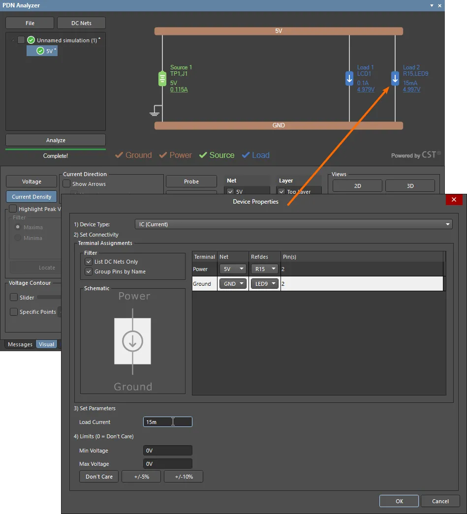
The PDN Analyzer also allows the stipulation of device pin connections for a load, which in turn allows the creation of multiple load models for a single component device that consumes different currents through different pins.
The LCD device in the example project demonstrates this situation, where its 5V connection at pin 15 (LED+) powers the display backlight, while the 5V connection at pin 2 (VDD) powers the internal logic – in practice, pin 15 will consume significantly more current than pin 2.
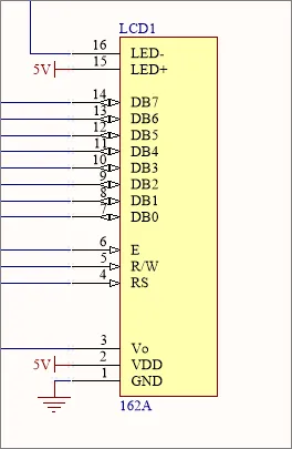
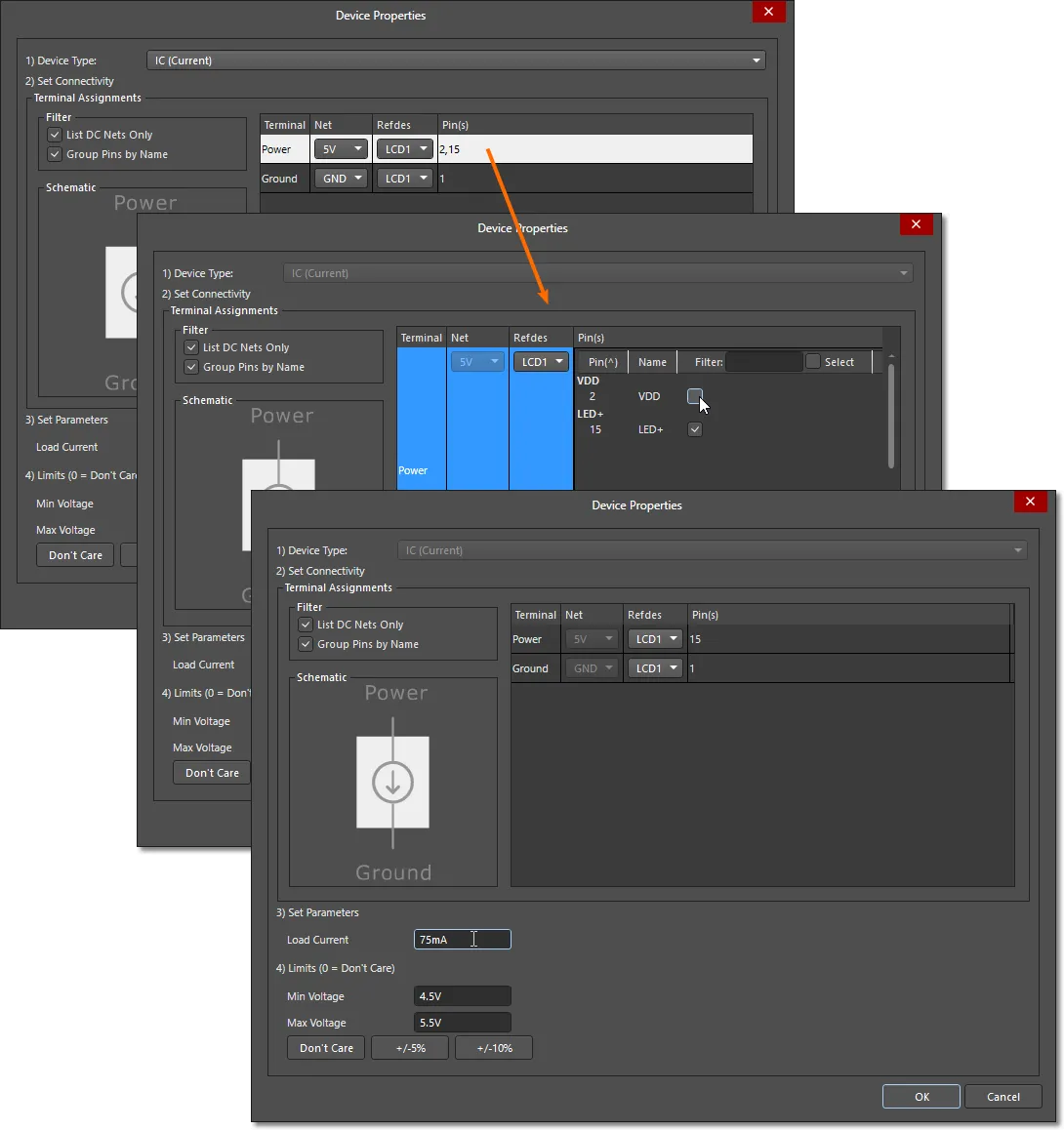
When previously added as a single PDNA load model, both pins for LCD1 were nominated (by default) as the 5V load connection, and the PDN analysis distributed the LCD1 load current equally between these pins. To improve the accuracy of the power analysis, the LCD1 component can be represented as two load models: one for each 5V pin and its associated load current. This change can be made by editing the pin parameters of the existing LCD1 load model, and then adding another load for the separated pin.
Open the existing LCD1 load model by double clicking on its icon in the network graphic to open the Device Properties dialog, then double click in the Pins(s) field of the 5V power net entry. The resulting pin editing mode allows the selection of individual device pins for that load. Deselect pin 2 to reconfigure the load for just pin 15 (LED+), and adjust the Load Current parameter for say 75mA to represent the LCD backlight current.
Next, create another 5V network load for LCD1 and set pin 2 as active (with pin 15 disabled) to represent the VDD load, which can be set to a suitably lower Load Current – say, 20mA.
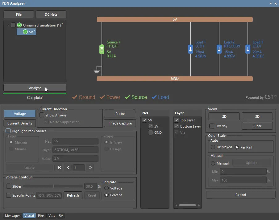
The 5V power network can then be re-analyzed to gain a more accurate representation of the LCD1 load through the network paths.
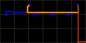
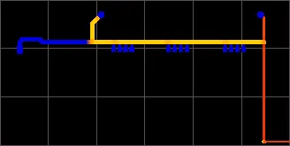
The difference in load current distribution can be seen when comparing the Current Density of the LCD1 power network tracks between the original and updated load arrangements. The below Current Density analysis images show the original, single load LCD1 model result on the left, and the updated multi-load result on the right.
Note the current density in the tracks supplying pins 2 (the LCD pad towards the left) and 15. The updated version correctly shows the majority of LCD current flowing to pin 15 (the LCD pad towards the right), rather than being evenly distributed between the two pins, as was the case (left image).
Simulation Settings
The results from an analysis, and in particular the degree of IR losses in the board shapes, will also depend on the specification for the board copper conductivity and Via wall thickness. To view and edit these settings select the Simulation tab in the Settings dialog – to access the dialog, right click on the current analysis name and select Settings from the context menu.

Metal Conductivity
The Metal Conductivity section of the dialog provides details and settings for the conductivity value (inverse of resistivity; 1/R) of the metal used in a design. The base conductivity (or resistivity), temperature coefficient, and/or temperature can be selected or modified in the dialog to reflect a design’s board construction properties:
-
Pure Copper – copper is typically assumed to have a conductivity of
5.88e7S/m at 25°C, and a conductivity thermal coefficient of 0.4%/°C. This positive temperature coefficient means that raising the Temp. Compensation setting in the dialog from 25°C to 125°C (100°C delta) will lower the simulation conductivity by 40%, to 3.53e7S/m, for instance.
-
PCB Copper – this is the default setting for simulations, and reflects conductivity values reported in industry literature as representative of the metal found in PCB electro-deposited (ED) copper, which is measured to be
4.7e7S/m at 25°C, with a thermal coefficient of 0.4%/°C.
-
Custom – choose this option enter specific Conductivity or Resistivity values for the simulation.
Note that the displayed Sim Conductivity figure represents the final conductivity value after taking into account all parameters – the Sim Resistivity figure is its inverse value.
Via
Set the dialog's Via Wall Thickness value specify the weight of the Via wall metal for all Vias in the design simulation analysis.
The setting can noticeably affect the power network DC losses due to the inherent resistance a thin-walled (-plated) Via represents. When of sufficient size/weight however, a Via will not impede a design's DC performance, and will show the same current density as the power traces it connects – and no significant voltage loss between its connection points. A DC analysis example of loss through Vias is shown in a section below.
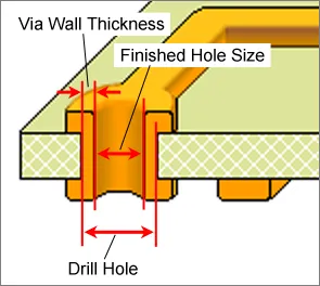
In terms of the simulation, the Via size and wall thickness effectively defines the amount of conductive material represented by the Via, and therefore its resistance/conductivity. The simulation assumes that the Via diameter represents the finished hole size, and the via wall thickness then increases the Via diameter. Therefore: Finished Hole Diameter + (2 x Wall_Thickness) = Drill Diameter.
Example 2
This example demonstrates how to implement a series of connected networks that can be analyzed as a whole, while taking into account the parameters of the series elements that interconnect them. It also provides an overview of adding Voltage Regulator Model (VRM) sources, which also act as interconnections between networks, and how a complete hierarchy of a design's power network is developed.
The example models the PWR_IN to 5V network of the SpiritLevel-SL1 reference project, and includes both the 3.3V (VCCO) and 1.8V (VCCINT) VRMs to create a complete power network structure.

The preliminary conditions for this PDN simulation example are:
-
the Spirit Level PCB project is open in Altium Designer
-
the PDN Analyzer application is active (Tools » PDN Analyzer)
-
the PCB design's DC Nets have been identified in the PDN Analyzer DC Net Identification dialog, as outlined above.
Begin the process of building up the example power network by specifying the input power net (PWR_IN) in a new simulation (select File » New Simulation, if required). As indicated by the project schematic, the PDN <Power Net> parameter is PWR_IN, <Ground Net> is GND, and the Source is J1.
Extending Networks through Series Elements
To model the full power path from the PWR_IN network to 5V network, the series fuse (F1) and switch (S1) components along with their intervening net need to be added. In the PDNA interface, these are added by sequentially extending the power network. Each net 'extension' is connected by a universal series element model.
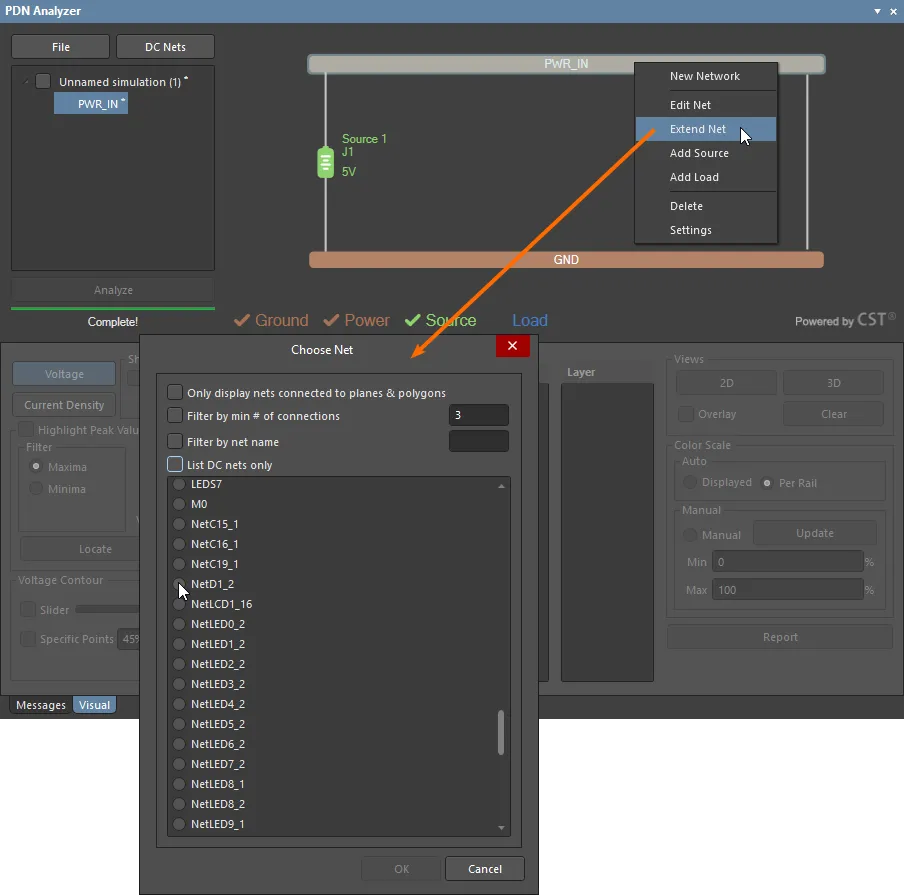
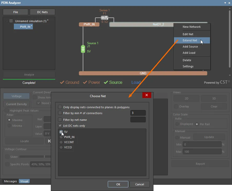
A net is extended by first right-clicking in the network you wish to add to and choosing the Extend Network option from the context menu. In the Choose Net dialog select the network that is connected to PWR_IN by a series element, which in this case is NetD1_2 – the network that bridges F1 and pin 3 of S1, which is identified as pin 2 of diode D1.
As this network is unlikely to have been registered in the initial DC Net Identification stage, deselect the List DC nets only option in the Choose Net dialog to expose that net for selection.
The net extension process will automatically add a Series Element between the two nets – double click on this element to specify its connectivity and parameters in the Device Properties dialog. The Series Element model is composed of a voltage source in series with a resistor, which allows the basic modeling of components such as Resistors, Inductors, Diodes and Switches etc.
In this case the Series Element is fuse component F1, which is selected as the connectivity RefDes options and given a nominal internal Resistance of 0.1Ω. If the Series Element was a semiconductor device, such as diode, the Voltage Drop parameter would be specified along with device's internal Resistance value.
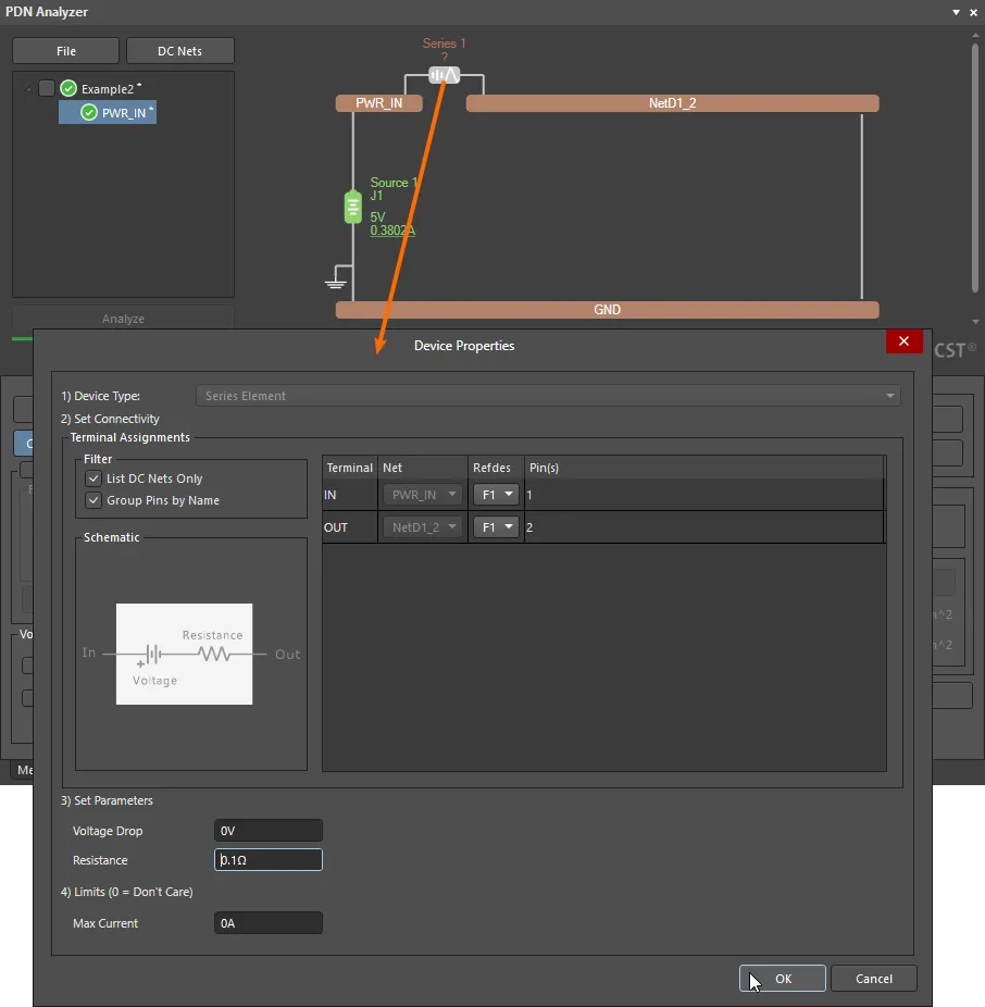
Following through the schematic, the next step is to extend net D1_2 to the 5V power net via switch component S1. As above, choose Extend Net from the right-click context menu and select the net to extend to in the Choose Net dialog.
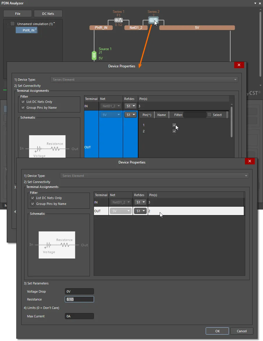
The added Series Element in this case is S1, which connects the D1_2 net to the 5V output network via pins 3 to 2 (see schematic). Since the spare input switch of S1 (pin 1) is tied to its output connection (pin 2), and does not carry load current, by way of example, pin 1 can be removed from the network analysis using the pin selection options of the Device Properties dialog – double click on the Pin(s) field of the OUT terminal entry.
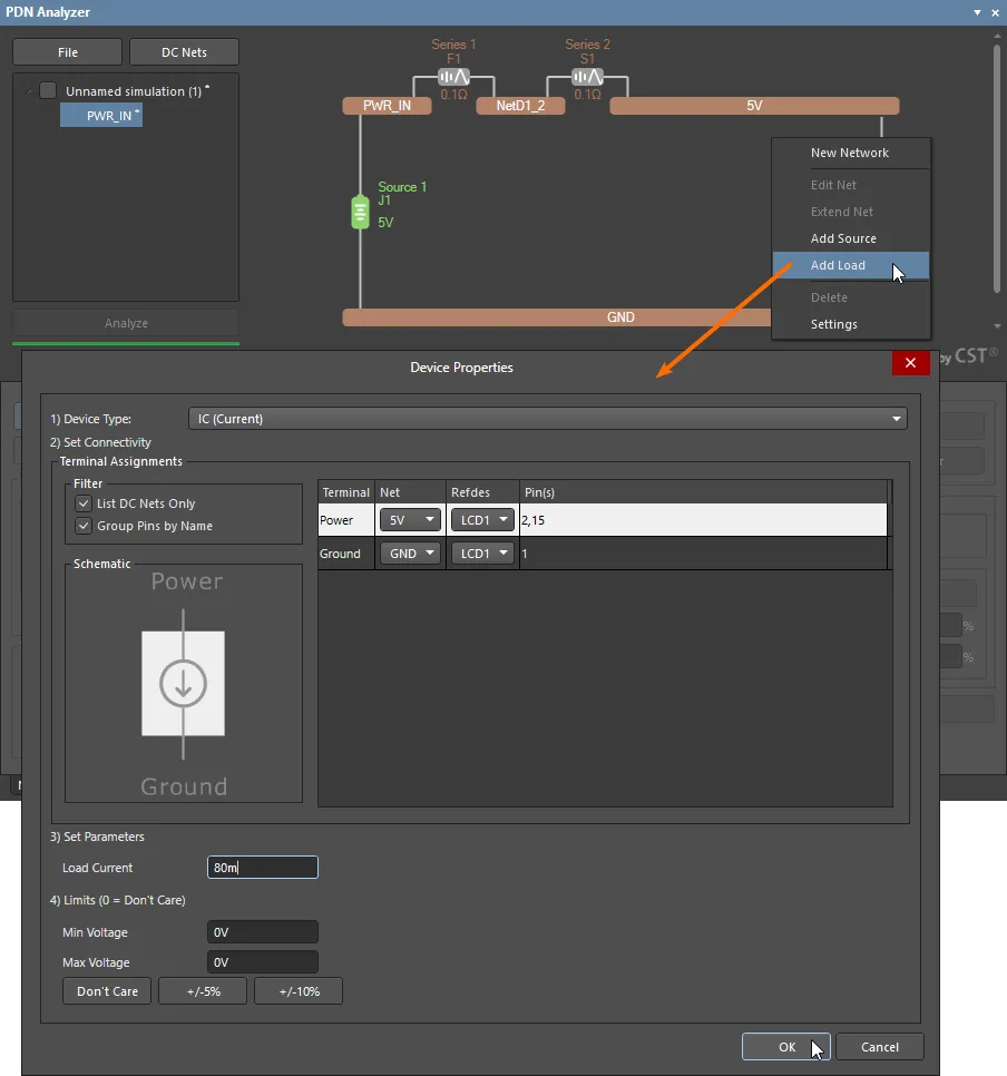
A load can now be added to the 5V section of the connected power networks – in this case, that of the display module LCD1.
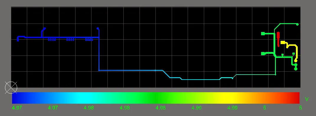
When the analysis is re-run, both the data and the graphic representation in the PCB Editor will include all three connected power networks, and show the computed current and voltage drop through the interconnecting Series Elements.
Including Voltage Regulator Models
The PDN Analyzer offers active Voltage Regulator Models (VRMs) that can be inserted between voltage input and output networks. When added to PDNA power networks, they manifest themselves as both a Load on the voltage input network, and a Source on the voltage output network. The VRM model options include Linear, Switchmode and remote-sensing Switchmode voltage regulators.
The SpiritLevel-SL1 reference project uses linear voltage regulators to produce the 3.3V (VCCO) and 1.8V (VCCINT) power supply rails. When the VCCO regulator (U3) is added to the PDNA simulation network, it is presented as a load on the 5V input network and as a Source for the 3.3V network.
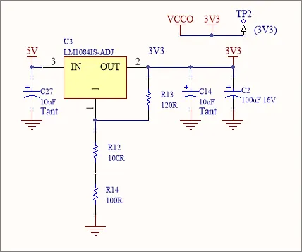
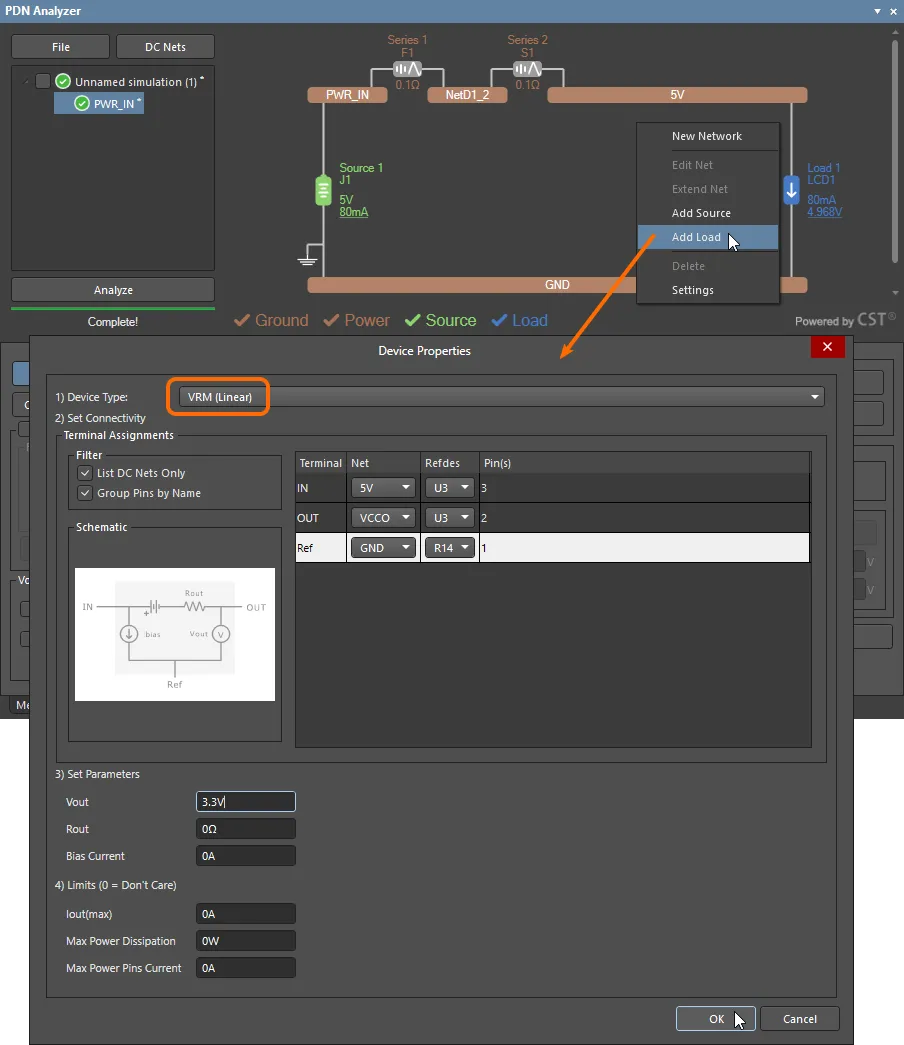
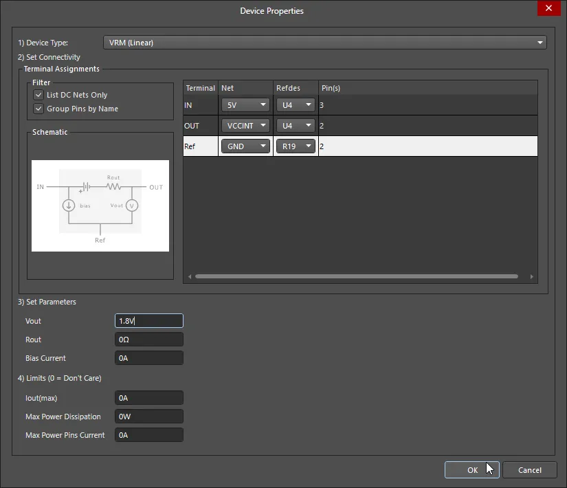
To place linear regulator U3 as a load on the 5V network (as implemented in the procedure above), add a Load to the 5V network and select the VRM (Linear) option as the Device Type in the Device Properties dialog. Set the model's connections as indicated in the schematic and specify the Ref pin as the GND connection of R14. This reference point could be at a different and perhaps more suitable location in the immediate area of the PCB, depending on the GND network layout.
To finalize the VRM, set its output voltage parameter (Vout: 3.3V), and optionally its output (internal) resistance, standing bias current and any Limits you wish to be detected during analysis.
The PDNA features a means to automatically add the VRM's output side model as a Source to the target output voltage net, and if necessary, create that network.
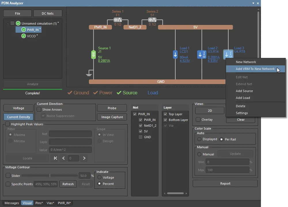
For the example case, right click on the VRM load model that was just created (Load2: U3) and select the Add VRM To New Network option. This will automatically create the VCCO network with the VRM (Source 1: U3) output side model as a voltage Source (3.3V).
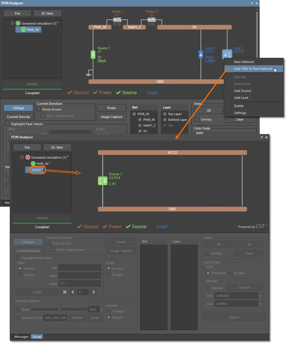
Note that the two manifestations of the 3.3V VRM, its input model as a Load on the 5V net and its output model as a Source for the 3.3V net, are interactive and effectively the same model. As such, the VRM may be accessed and edited from either network in the PDNA interface.
The new VCCO network can now be selected and a suitable Load added. For the example, this is a 0.2A load current drawn by multiple pins of component U1.
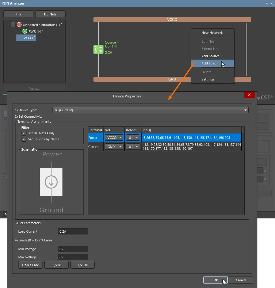
The completed power network arrangement now includes two networks (PWR_IN and VCCO) connected together by the 3.3V Linear type VRM. When the top level of the network hierarchy is selected in the current PDNA file structure, the network graphic provides a block style overview of the power net interconnections.
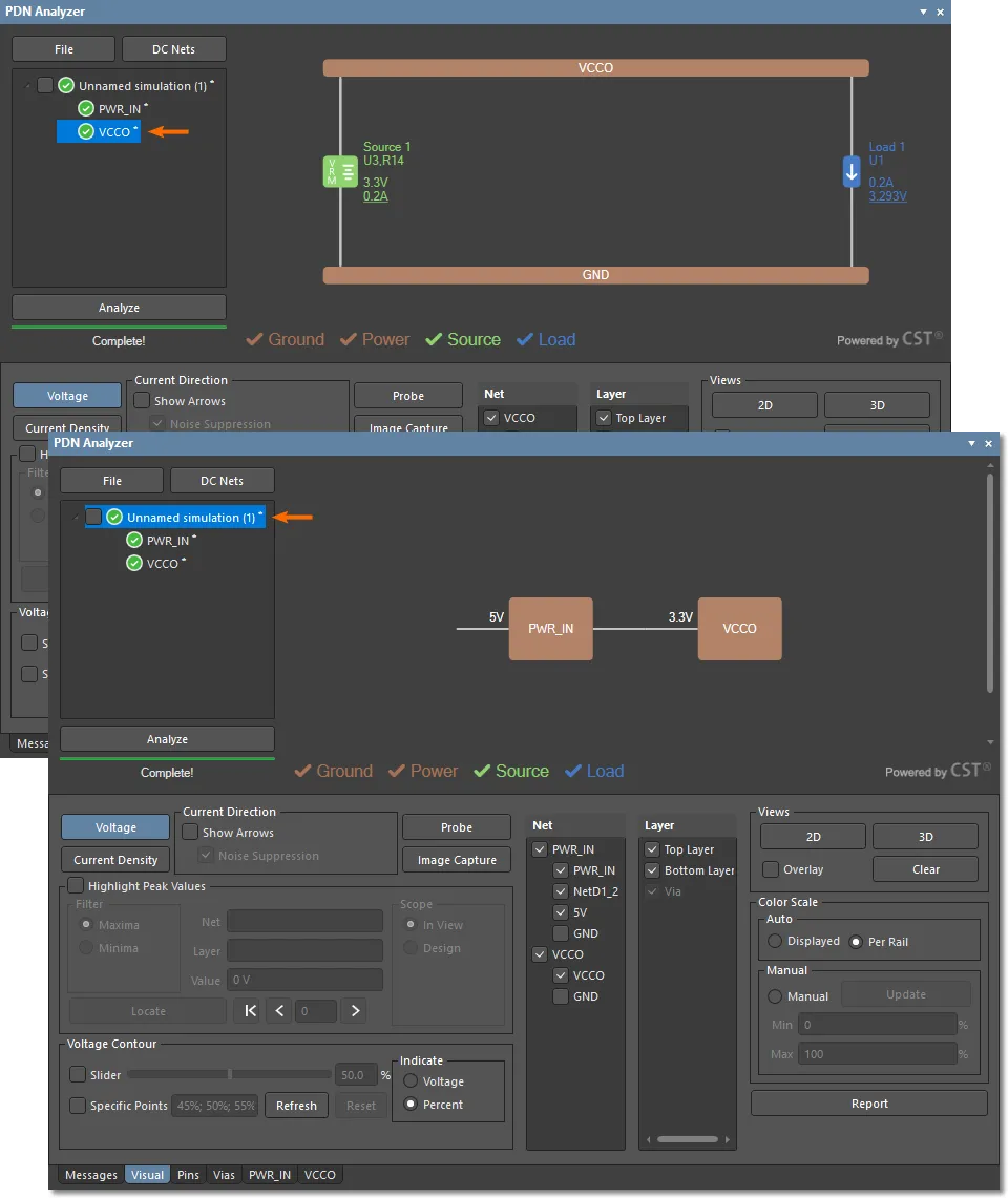
In this example the VRM was added as a Load to the 5V (input voltage) network, and then used to automatically create the 3.3V (VCCO) voltage output network with the VRM as a Source. The reverse of that process is also possible, and may be more convenient in some cases. Then, the VRM is added to the output voltage network as a Source, and that model is added to an 'input' voltage network as a Load (Add VRM To New Network or Add VRM To Existing Network).
A PDN analysis will yield results for the composite network, including the VRM. Graphically, the PCB Editor will display all networks when the top level of the network hierarchy is selected in the PDNA interface. Select an individual network in the listing to constrain the rendered graphic to that network, and toggle the lower panel's Net and Layer options to further control the view.
Note that the example's GND network path will now include return current contributions from both the PWR_IN and VCCO networks.
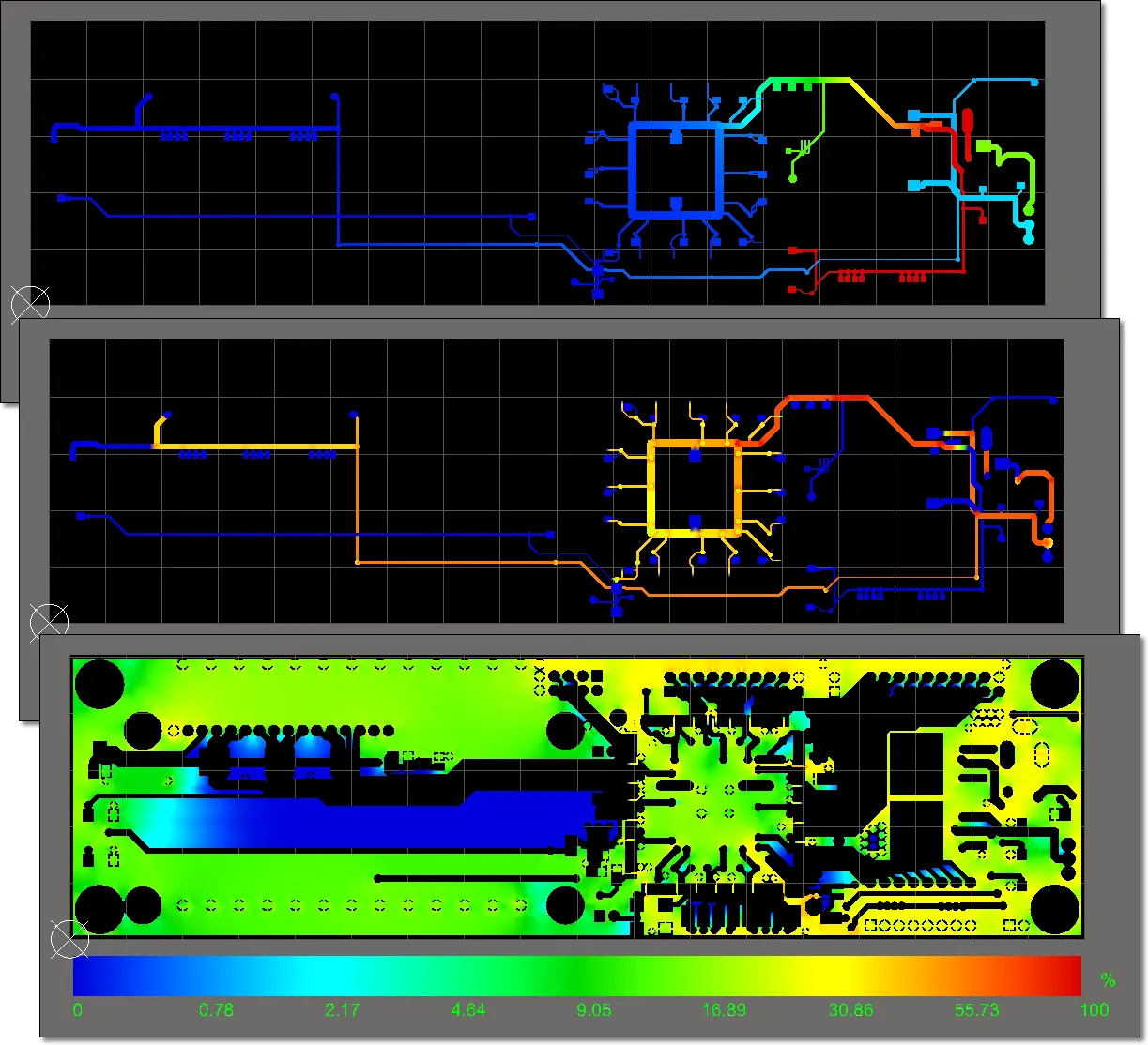
The example project's power distribution network can be completed by adding the remaining VRM (U4) and its 1.8V power output network (VCCINT).
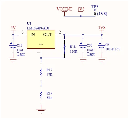
Add a Linear VRM to the 5V network as previously described, and set its Vout parameter to 1.8V.
Add the VRM (here, Load 3) to a new network to create the 1.8V (VCCINT) power network.
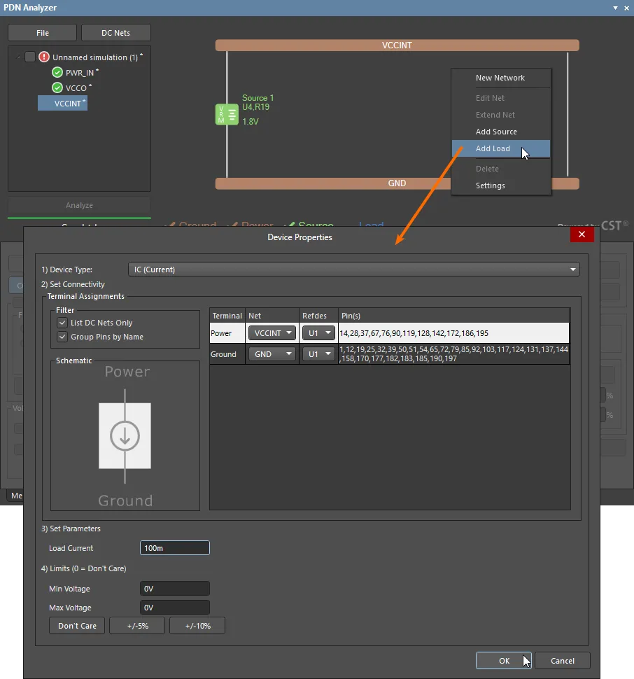
Add an appropriate Load to the VCCINT network – here, the 1.8V power pins of component U1.
The PDNA interface network hierarchy will now show all three interconnected networks.
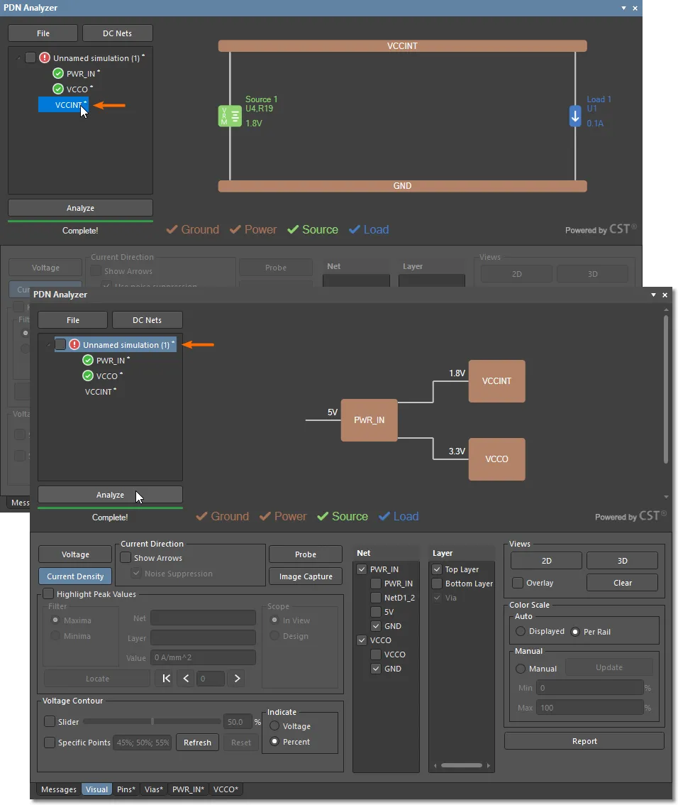
A PDN analysis will yield results for the composite network, including the VRMs.
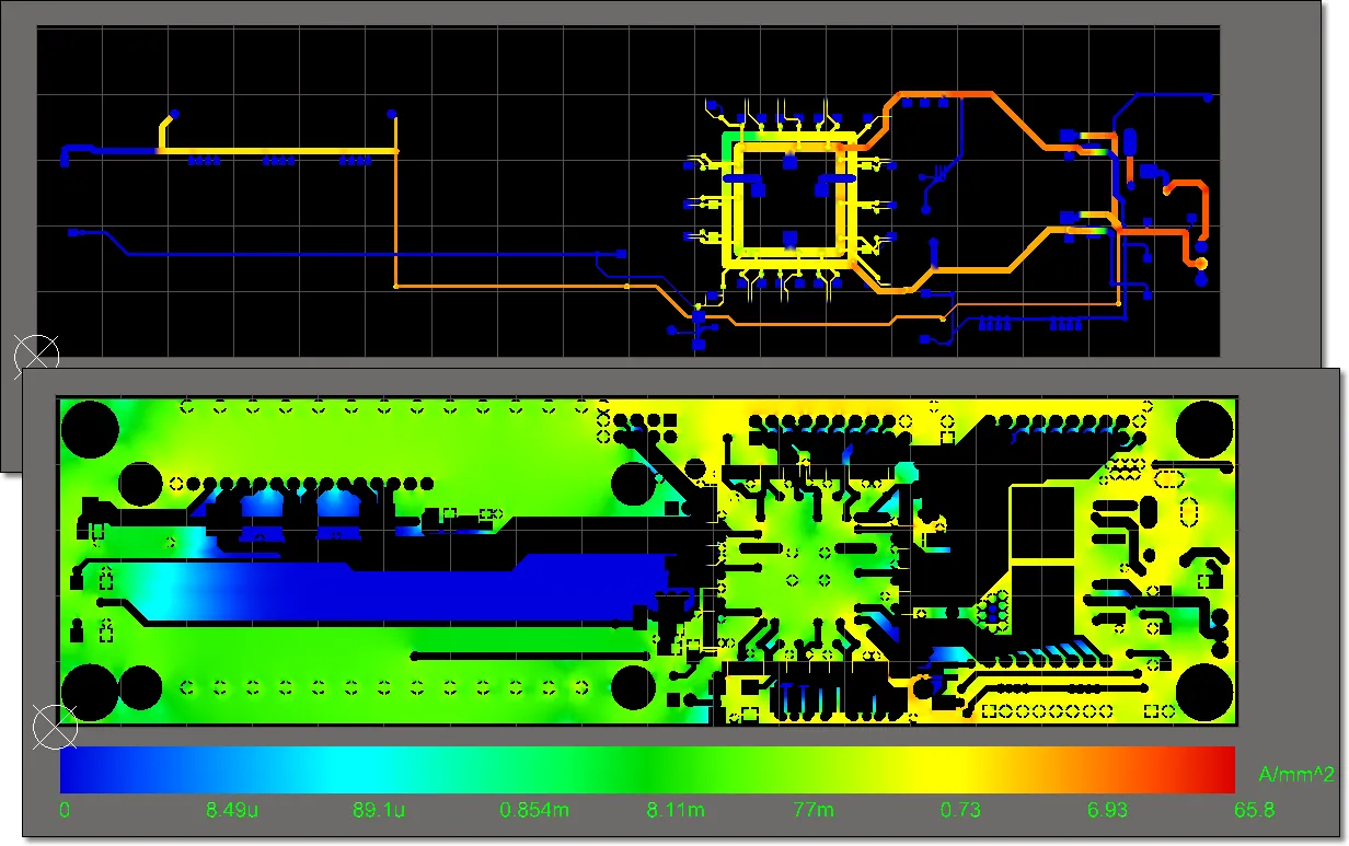
Again note that GND network now includes the return current for all three networks, which use the common GND layer shapes. Its maximum current density level (65.8 A/mm2) is now high and likely to exceed acceptable limits.
Locating Power Integrity issues
The PDN Analyzer offers a comprehensive range of graphical and data information that can be used to assess and troubleshoot the power integrity of an analyzed PCB design.
Taking the example shown above, the analysis of the Top Layer GND network path indicates the presence of an unacceptably high current density, as indicated by the maximum scale reading of 65.8A/mm2. The location of the problem area is not immediately obvious, but can be exposed using the PDNA’s Highlight Peak Values feature.
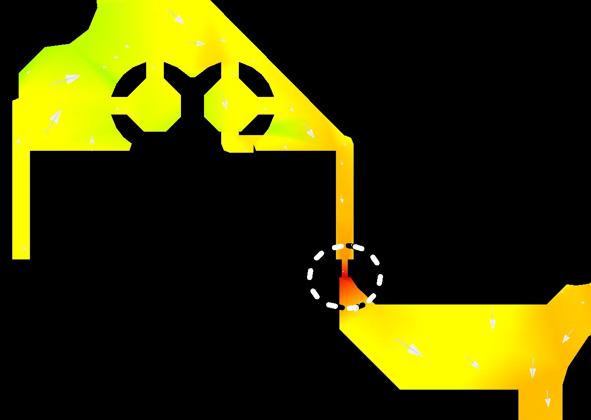
When selected, with the Filter option set to Maxima, the peak Current Density area will be highlighted and marked on the analysis graphic in the PCB Editor.
Click the  button to repeat the graphic highlighting, or use the associated buttons (
 ) to step through the highest peak readings/locations in order. Set the Scope options to include highlight peaks in the PCB area that is currently visible (In View), or all those for the entire layout (Design) – the latter option will pan and zoom to each location as you step through.
Further information about an area of concern can be deduced by enabling the PDNA's Show Arrows feature, which overlays multiple arrow graphics that indicate current direction (the arrow's angle) and the relative magnitude (the arrow's size) at that location. For this example it confirms that the high density area is the current return path from U1 (at the top) to the GND area at lower periphery of the board.
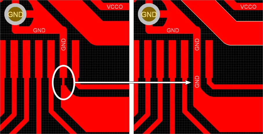
One way to resolve this issue is to increase the width of the track in the area of concern.
The PCB edit can be completed while the PDN Analyzer is active, which allows iterative layout improvement to be completed and then re-analyzed. Click the Clear button in the Views area to disable the PDNA results in the PCB Editor and proceed with the required PCB edit.
The PDN analysis can then be repeated (click  ) to check the power integrity results. The below two images illustrate the change in Current Density through the GND network (on the
 Top Layer) due to the increase in track width at that critical point – the upper image shows the initial Current Density result, while the lower image shows the Current Density graphic after the PCB modification.
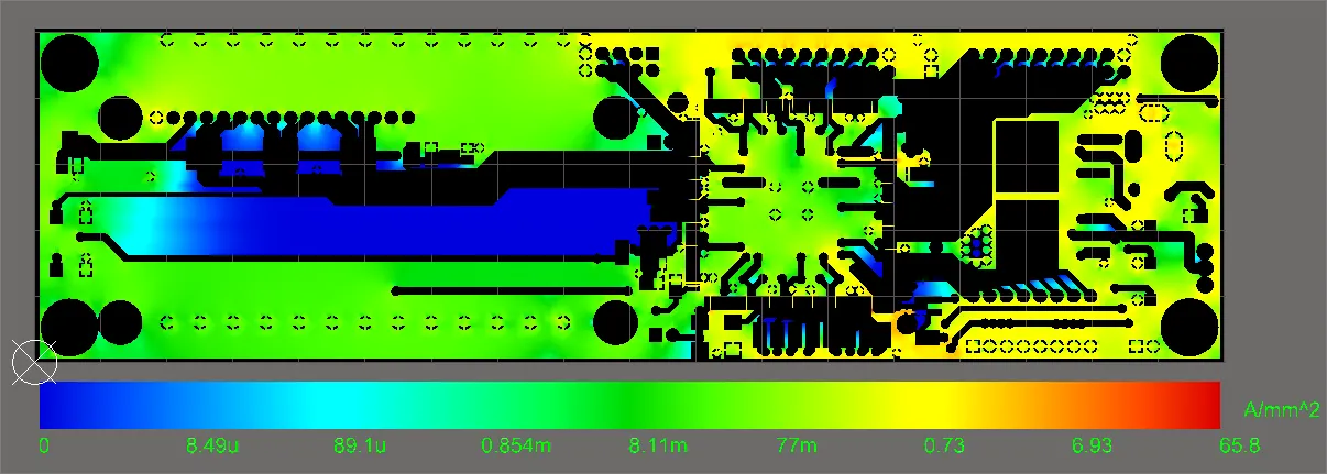
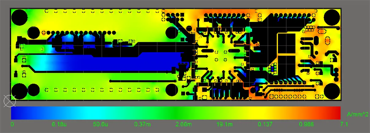
Points of note in this before (top image) and after (lower image) comparison are:
-
The maximum Current Density level in the GND layer has reduced to an acceptable level of roughly one-tenth of the previous value –
65.8A/mm2 to 7.1A/mm2.
-
The maximum current areas, which are now much lower values, are more evenly spread through the GND return paths rather than focused in one problematic location.
-
For a more literal graphic comparison, manually set the Current Density scale to the previous value – select the Manual scale option, enter
65.8 in the Max field and click the  button to refresh the display.
Current Density Limit Violations
A more objective way of locating and resolving power integrity issues in the current paths of a PCB design is to define specific Current Density limitations that will trigger a violation when exceeded. See below for other types of violations.
Current Density limits for Surface/Internal Layers and Vias are specified under the Limits tab in the Settings dialog, which is opened by right-clicking on the current PDN simulation Name and selecting Settings from the context menu. The imposed Limit settings will apply to all Surface/Internal Layers and Vias in the board design.
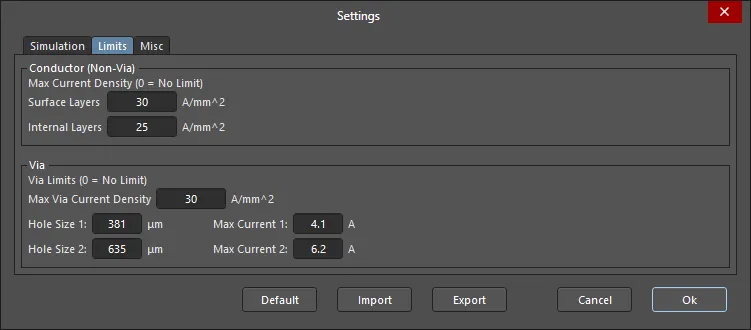
The specified Current Density limitations apply to the results of the current analysis, and can be altered and reassessed without the need to re-run the simulation – the Limit detection is a post-analysis process. Any networks that contain violations are shown with a dashed red outline.
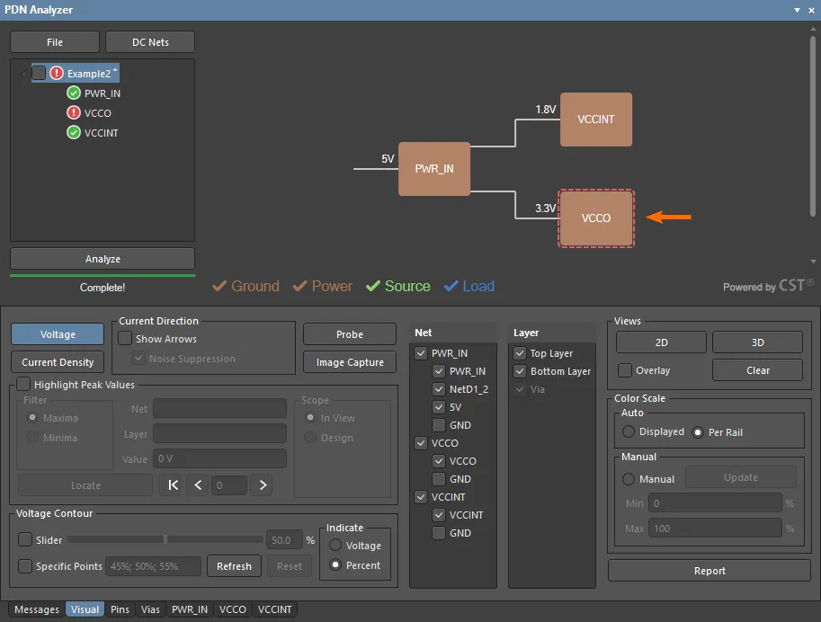
In the example case shown here, the VCCO power network contains Current Density violations. When the VCCO network itself is selected, the VCCO power path is shown to be in violation by its highlighted outline.
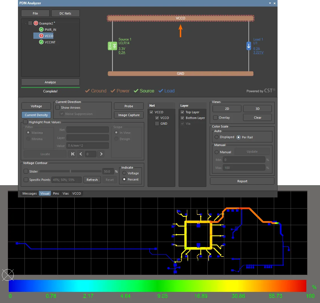
Hover the cursor over the violating network to expose a pop-up list of its current violations and their associated details. The single entry in this case indicates that the Current Density in a Via (approx. 34.5A/mm2) is in excess of the defined limit (30A/mm2).
Double click on the violation entry to cross probe to (pan and zoom to) its location on the board. In the below image, the PDNA graphics view is set to 3D mode, which more clearly presents the Via of concern and its Top/Bottom Layer connections.
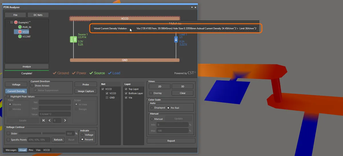
Note that for the purposes of demonstrating a single Violation, the Via has been reduced in size in
Spirit Level project board design.
The related data for this Via, including an indication of its Current Density violation, is available under the Via tab of the PDNA interface.
The Via information listing applies for all networks included in the current design. Toggle the Net and Current Density column headings to arrange the listing to show VCCO network Vias ordered by Current Density. Any Current Density values that exceed the defined limitation will be highlighted in red.
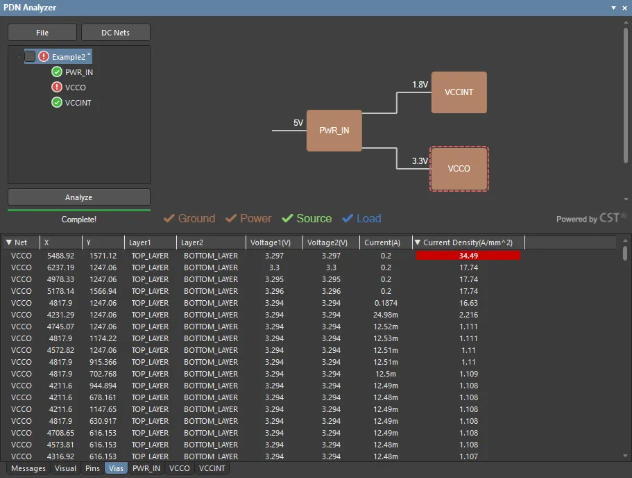
Double click on any entry in the Via list to cross probe to its location on the PDNA board graphics.
Other Violations
Along with the detection of specified Current Density limits, the PDN Analyzer will also detect targeted network performance violations, such as any Limit parameters that have been specified in the simulation configuration when adding a Load, Source or Series Element.
These simulation Limit parameters include:
-
The acceptable voltage range at a Load
-
The maximum output current from a Source
-
The permitted power dissipation in a Linear Regulator Source, and its maximum output current.
-
The maximum output current from a Switchmode Regulator Source.
-
The maximum current through a Series Element.
Unlike network element simulation parameters (such as Source voltage or Load current settings), which are processed during the analysis is run, the detection of any Limit parameter violations (such as the specified minimum voltage at a Load) is a post-analysis process. This means that a change the value of a Limit parameter will be detected immediately, without the need to re-run the simulation analysis.
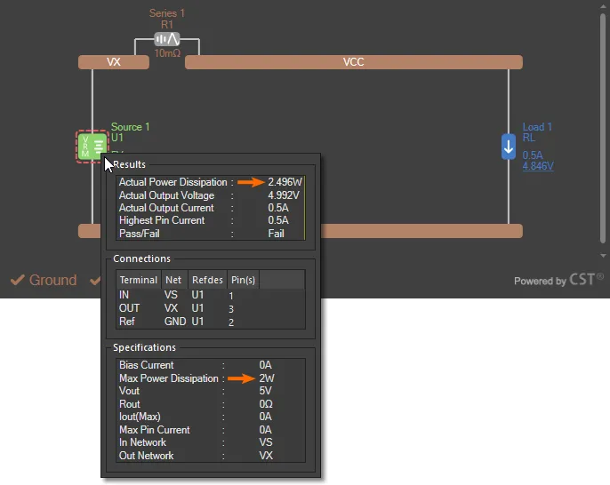
Where a Limit parameter has been specified (has a non-zero value), a violation of the parameter will cause the offending network element to be highlighted in the PDNA interface network graphic. Hover the cursor over the element to see its parameters and analysis results.
In the example shown below, the computed power dissipation in Source 1 (voltage regulator U1) has exceeded its defined maximum Power Dissipation parameter of 2W.
More detailed information on the performance of a power network is available under its network tab, which presents a tabular view of the analysis results data and includes computed network power consumption values.
Example 3
This example demonstrates the application of PDN Analyzer’s Switch Mode Power Supply (SMPS) simulation models (VRMs) in a power network, and shows how an updated network model can deliver a more accurate power analysis result. The example also provides an overview of using the PDNA’s Voltage Probe and Contour features to show the voltage data at specific points or areas in the board layout shape.
The example is based on Altium’s DB46 Xilinx Daughter Board reference project, and focuses on the SMPS section (U5) used for the design’s 1.2V power supply network (1V2).
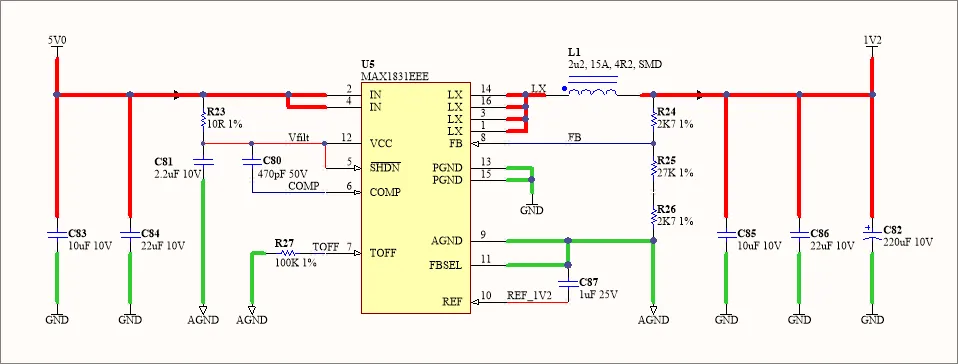
Again, the preliminary conditions for this PDN simulation example are:
-
the DB46 Xilinx Daughter Board project is open in Altium Designer
-
the PDN Analyzer application is active (Tools » PDN Analyzer)
-
the PCB design's DC Nets have been identified in the PDN Analyzer DC Net Identification dialog, as outlined above. Note that for this example, networks
LX and AGND are also required.
Begin the process of building up the example power network by specifying the input power net in a new simulation (select File » New Simulation, if required). As indicated by the above schematic, the PDN <Power Net> is 5V and the <Ground Net> is GND. The Source for the 5V network is connector header HDR_T1 or HDR_B1.
Switch Mode VRM
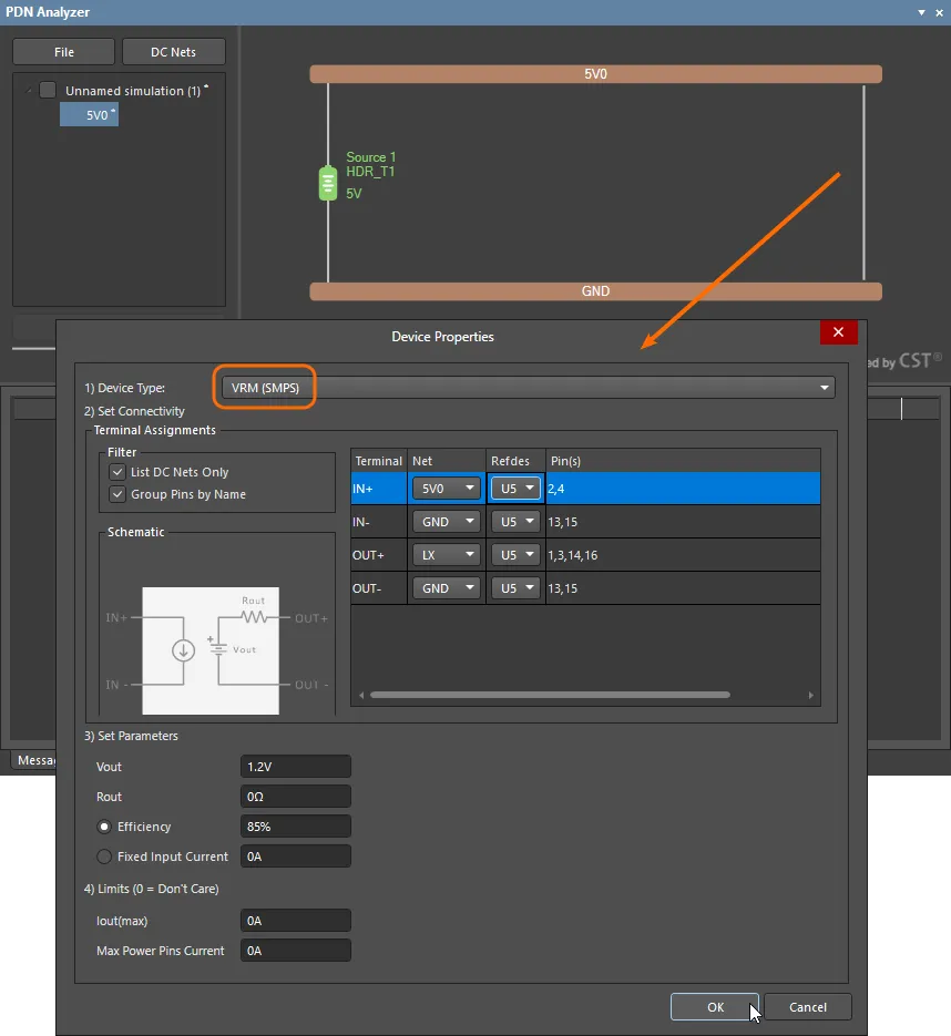
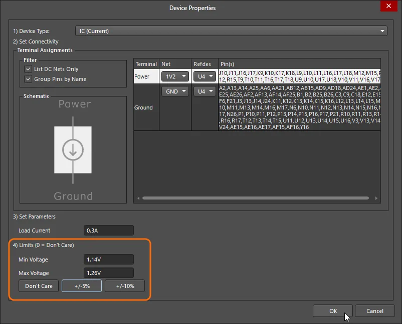
The model for the design’s SMPS circuitry is added to the 5V power network by choosing VRM(SMPS) as the Load Device Type in the Device Properties dialog. As indicated by the model’s schematic in the dialog, the IN and OUT pin sets are separately defined.
To correctly define this model for the circuit, specify LX as the output, U5 for the RefDes options and 1.2V as the Vout parameter – as shown in the above schematic. Optionally set the Rout and efficiency/current parameters to correspond to the SMPS device used.
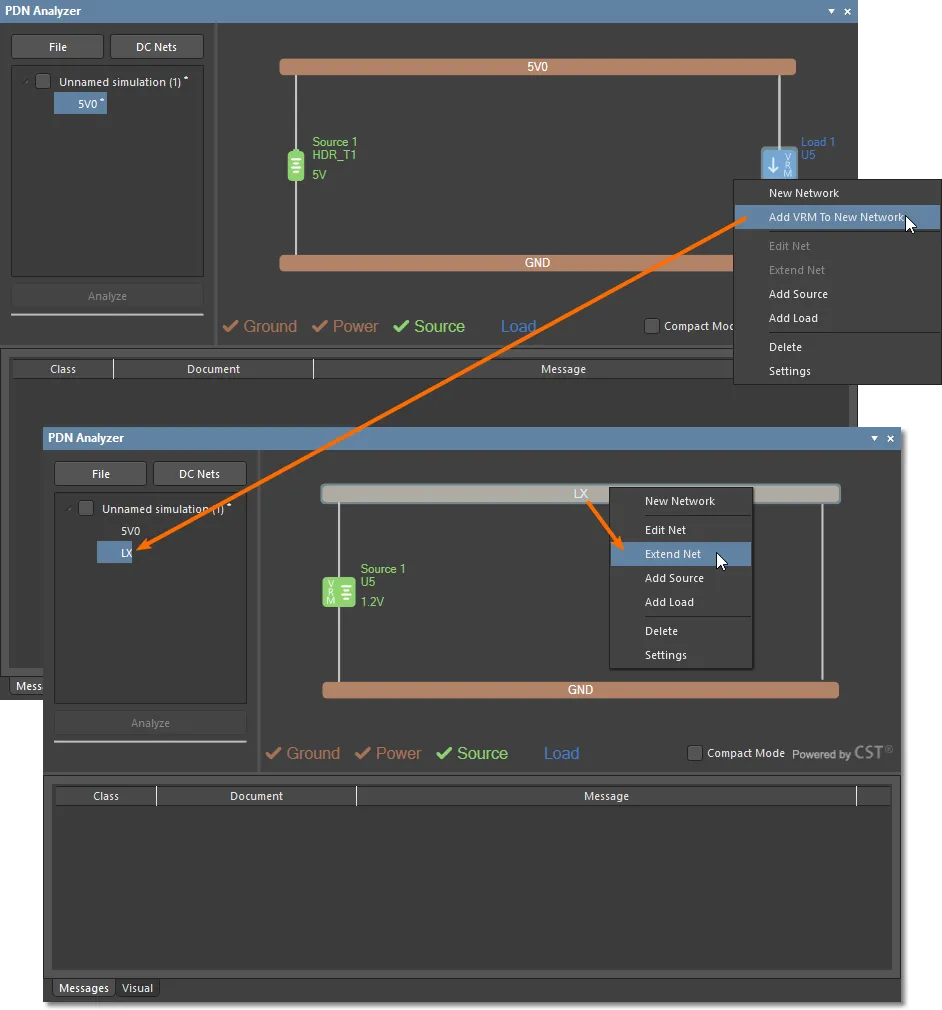
Complete the SMPS model implementation by adding the VRM to its output network (Add VRM To New Network), which will be selected as the LX network automatically. The LX network can then be extended to include the 1.2V power network, as per the schematic.
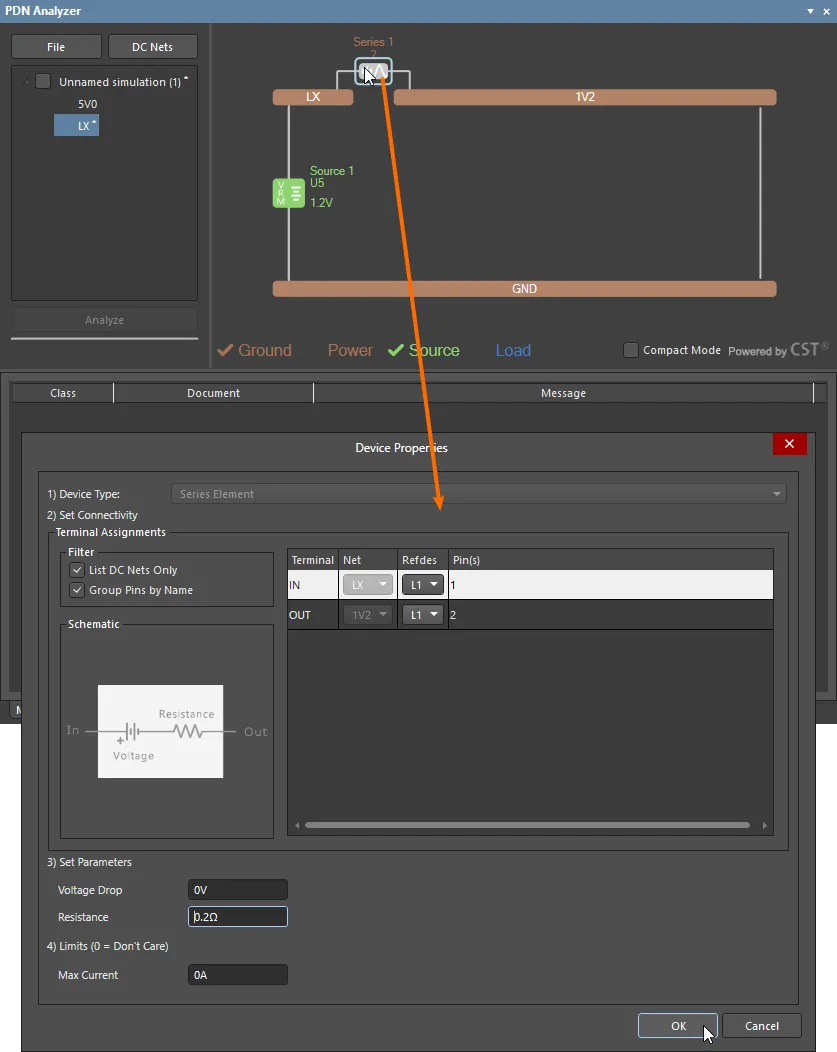
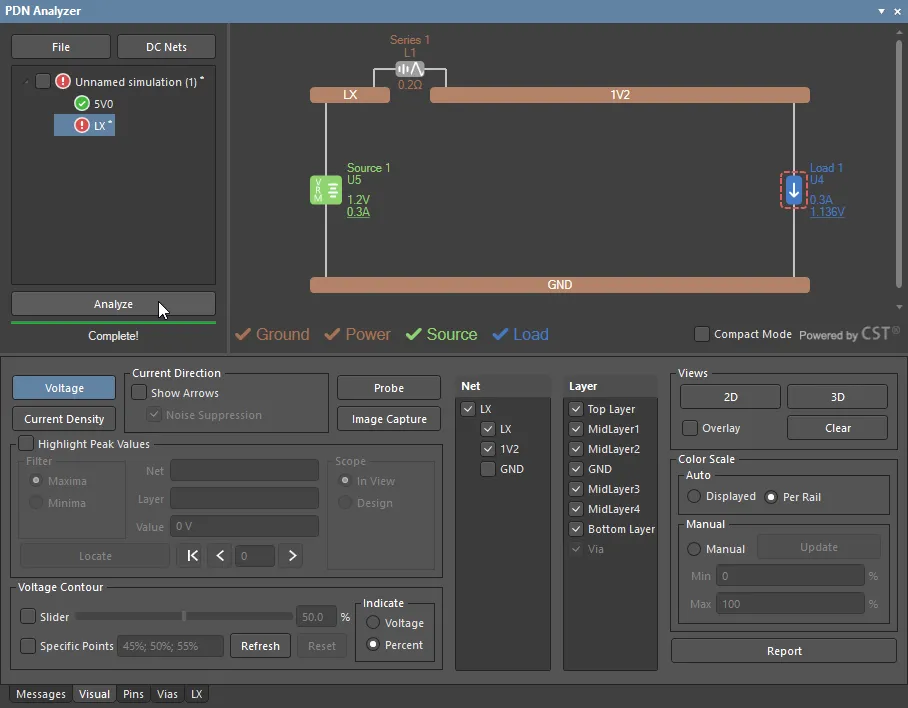
The LX and 1V2 networks are linked by Series Element L1 (the SMPS buck inductor), which should be set to exhibit an appropriate series resistance. This is set to a somewhat high figure of 0.2Ω for the purposes of this example.
Lastly, add U4 as a 0.3A Load on the 1V2 network and specify an acceptable load voltage deviation of +/-5%. Note that the Current Density limit options under the Limits tab of the Settings dialog should be set to 0 (the default No Limit condition) for this example.
Run the analysis and note that the Load on composite network LX indicates a Violation, which is due to the 1V2 network voltage at the load (U4) being unacceptably low (around 1.14V).
Data Probe
Along with the visual interpretation of the PDNA graphic and Scale in the PCB Editor, the PDN Analyzer offers a number of tools for interpreting the analysis results at specific area or points in the design layout, such as the active Probe.
The Probe tool allows the Voltage or Current Density data at nominated points in the design layout to be recorded and compared. The versatility of the tool provides a method to accurately judge the analysed data results on any network or layer. For this example however, it can be used to confirm the source of the unacceptable voltage drop at the 1V2 network load – which is clearly due to the resistance of the L1 Series Element.
To perform a difference probe reading for the voltage on the 1V2 network, first set the PNDA to display only Layer MidLayer 1 (which is the main 1.2V path to U4), and Net 1V2. Select the  button to open the Probe dialog and enable the first probe location (
 ). Use the cursor crosshair to nominate the highest voltage point (the source of the
 1V2 network on this layer), then check the probe's Difference option and nominate the second location ( ) – the lowest voltage point, at the
 U4 load.
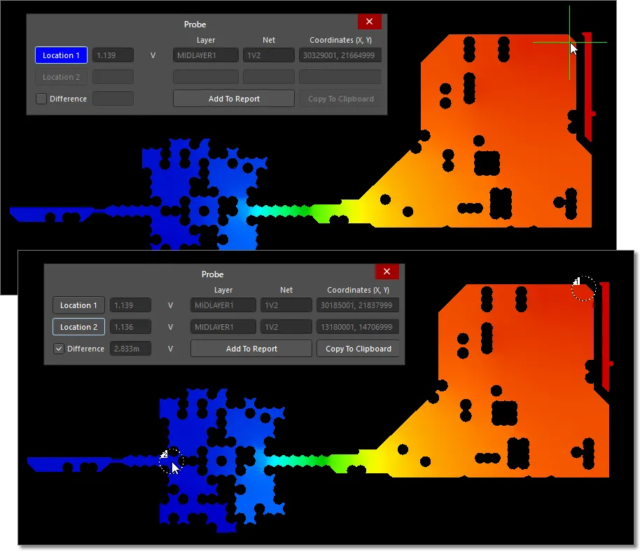
Note that the probe’s Difference reading indicates a voltage drop of only about 3mV for the network path. Similarly check the LX network path (Top and Bottom Layer active), which will show a voltage drop of around just 0.5mV.

Performing a probed Voltage Difference test between the two networks (Net LX and 1V2 enabled, Top and Bottom Layer) shows a 60mV drop across inductor L1, which is the primary voltage loss that triggers this particular analysis Violation.
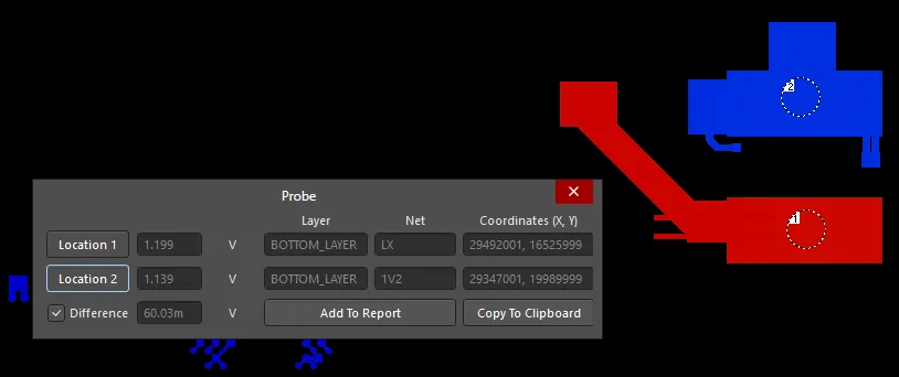
While voltage Probe investigation shown here has ascertained the primary cause of the IR losses in the power network, it could have been resolved more directly by inspecting the device pin voltage data under the PDNA’s Pins tab. The Probe feature is ideally suited to more detailed investigations where its location precision can be used to full advantage.
SMPS-sense VRM
The Switch Mode power supply circuit used in this example would normally use an inductor (L1) with a much lower resistance value, however the analysis results here do highlight that the basic SMPS model cannot take into account losses through L1 – generally though, this would not be an issue in a practical circuit.
In the example project's SMPS circuit, the voltage feedback sensed by U5 (at pin 8) is derived from the resistor chain R25–R26, which is between the 1V2 output network and the analog ground network AGND. The latter is linked to the GND network via a 0Ω tie resistor R118.
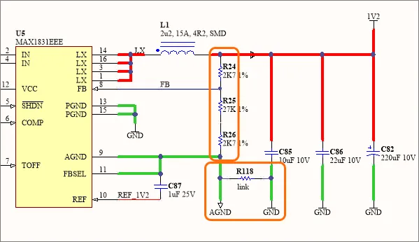
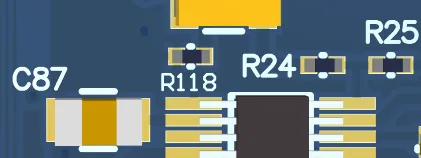
Note that for the purposes of this example, the source
DB46 Xilinx Daughter Board reference project has been modified to include a resistor-based network tie (
R118) between the
GND and
AGND networks, in place of the direct copper connection.
To more accurately model the circuit behavior around U5, the PDNA’s remote sensing Switch Mode model can be applied in place of the standard SMPS device. This model offers separate voltage sensing terminals (S+ and S-) that can be ‘attached’ to any pins on the specified output networks – such as those of the voltage sensing resistor chain in this circuit.
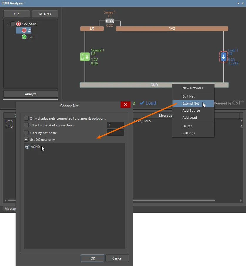
The first step in creating a more complete network model for the U5 SMPS circuit is adding the AGND network to the existing GND network. Use the Extend Network option and select the AGND net.
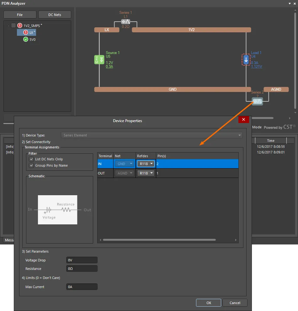
The AGND network is linked to the GND network via resistor R118, as shown in the above schematic, which should be set for a Resistance value of 0Ω.
To update the SMPS model in the LX network, delete the existing U5 source device (Source 1) and then add the alternative SMPS Sense model in its place. Set the model’s IN and OUT terminal connections as before. The sensing terminals (S+/S-) are set to each end of the circuit’s feedback resistor chain as indicated in the schematic.
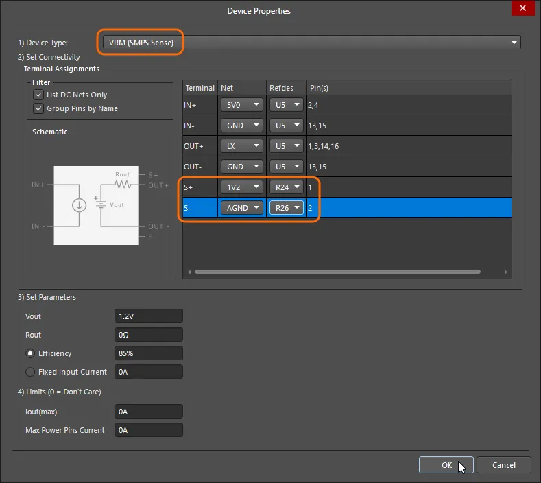
Propagate the replacement SMPS model from the LX network to the source 5V network, so that the networks correspond, by deleting its U5 Load and then applying the Add VRM To Existing Network » 5V Source option in the LX network.
The updated circuit can then be re-analyzed to assess the results. As shown in the below image, the load voltage is now well within the +/-5% requirement and does not indicate a Violation. In response to sensing the output voltage at the 1V2 network, the SMPS has compensated for the voltage loss in Series Element L1 – as such, the voltage at the LX network is 60mV higher.
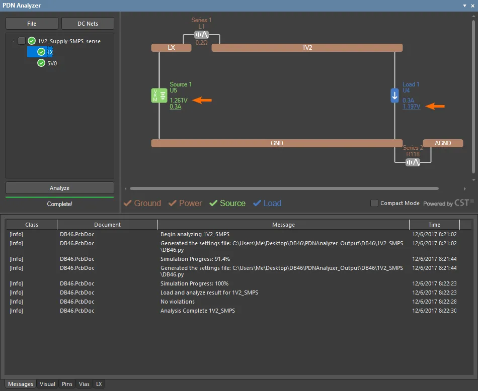
While using the advanced SMPS-sense model for this particular circuit yields more accurate analysis results, the practical use of SMPS devices with remote sensing capabilities may involve direct PCB connections from the sense terminals the load itself, rather than a nearby feedback network. In this case both sense lines (S+ and S-) would be run through dedicated PCB tracks to or near their respective ends of the load.
Voltage Contour
The decision of where to best place SMPS remote sensing lines (as outlined above) is one of the many possible uses for the PDN Analyzer’s Voltage Contour feature, which graphically indicates key voltage transition points in the board layout.
The feature enables an overlay of dashed voltage contour lines through the displayed layer(s) in the PCB Editor graphics. Multiple contour lines can be specified and displayed as either a percentage of the network voltage drop, or as literal voltages – see the Indicate options.

Along with the set of contour lines at specified percentage points, a further line may be included using the Slider option, which provides a continuous adjustment method of setting a line transition point.
To determine a suitable positive load sensing point for a SMPS for example, it would be desirable for the sense line to connect within less than say, 20% of the voltage drop at the load. For the SMPS-sense example shown above, a sense line track from U5 (S+) would connect to the 1V2 network power shape at any convenient point between the U4 load pins (to the left) and the 20% voltage contour line.
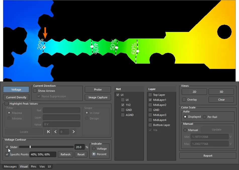
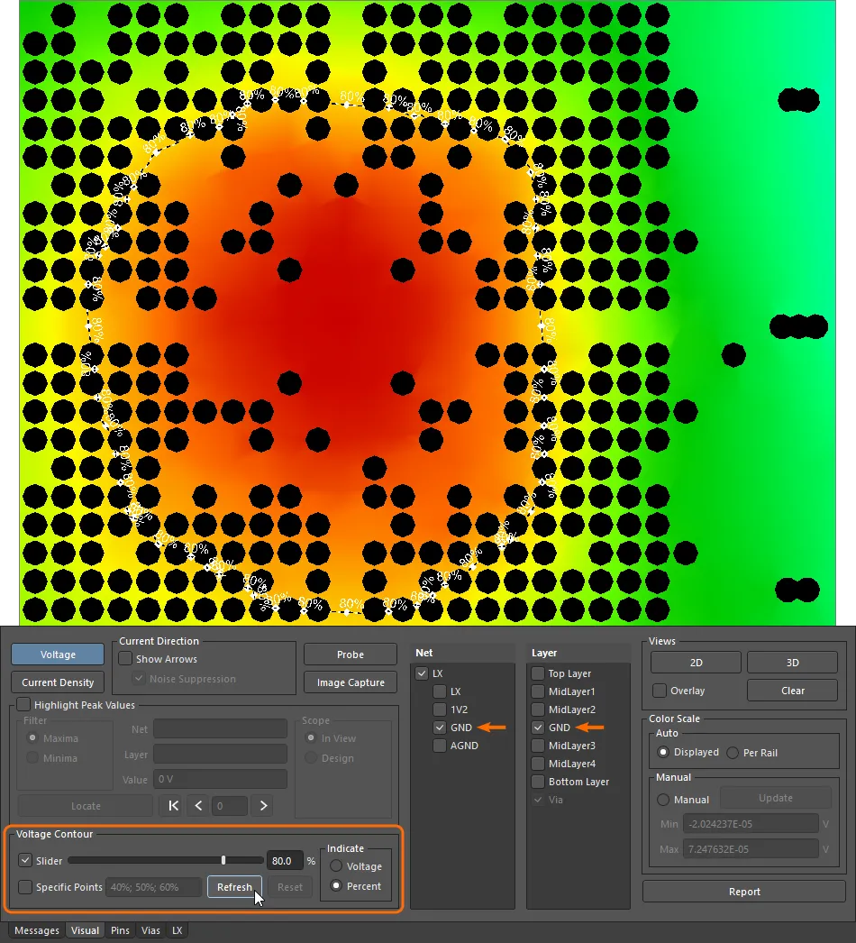
Similarly, to determine suitable pickup locations for the negative sense line (S-) of the SMPS (U5), a Voltage Contour line of say, 80% might be set for the load (U4) return path in the GND layer. In this case, since it is a negative load return current, the desirable ground shape location for the negative sense line connection would be within the perimeter of the 80% contour line.
Analysis Report
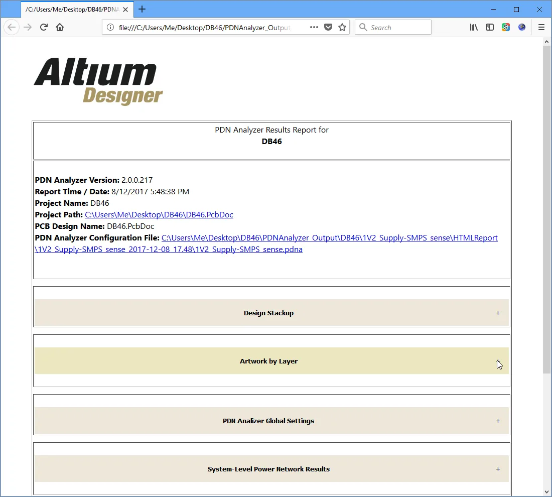
To store the results of a power integrity analysis for further examination or distribution to stakeholders, the PDN Analyzer offers a data and documentation Report function. The Report feature generates a very comprehensive HTML-based document that includes graphics and data for both current analysis results and the board design itself.
Select  button to configure the Report options in the HTML Report dialog. Check the Results inclusion boxes to set the degree of detail included in the Report and review any captured images to be included in the Report folder (
 ) – use the
  button in the main interface to capture analysis result images.
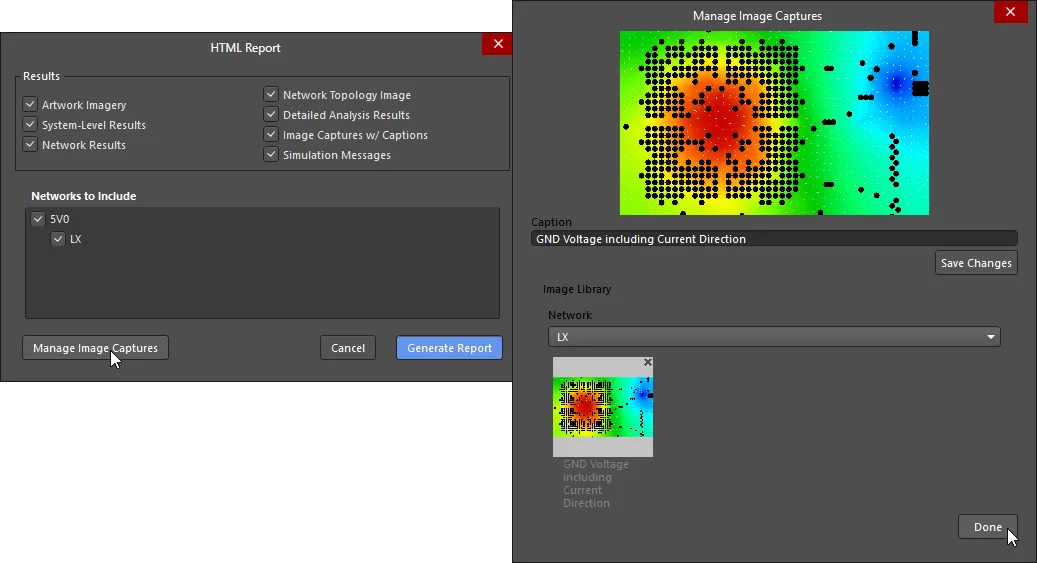
Click the  button to generate the interactive HTML Report and open its host folder, which will include all images (including those captured) and the related analysis configuration file (
*.pdna).
