A key ingredient of good board design is component layout. In a large design, a component's position on the board may have no relationship to its designator. For example, R1 may end up on the opposite side of the board to R2. To make it easier to locate a component on the board, you can reassign the designators (re-annotate the board) positionally.
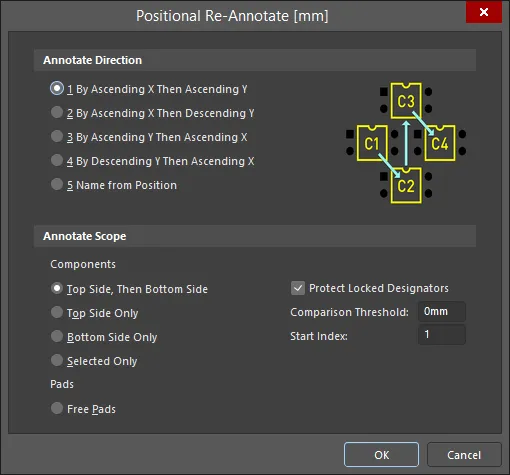
To systematically assign designators of targeted components, or free pads, in the PCB Editor based on their position, click Tools » Re-Annotate to open the Positional Re-Annotate dialog as shown below. Use this dialog to configure the scope of annotation (components (further targeted by side, or selection), or free pads), the direction of annotation (based on object position), and additional options, such as a starting index, and whether locked designators should be protected.
As you select a style of annotation, a graphical depiction is shown within the dialog as a visual indication of how annotation will transpire.

The Positional Re-Annotate dialog includes a graphical representation of each method.
Options and Controls of the Positional Re-Annotate Dialog
Identifying the Component Location
Each component is identified by its bounding rectangle, excluding strings. The components are sorted into a list and the list is renumbered in that order to create the new component designations. To compare two components in the X-direction, the left-side of the bounding rectangle is used. To compare two components in the Y-direction, the edge used depends upon the renumber direction: ascending-Y, use the bottom edge; descending-Y, use the top edge.
The Comparison Threshold option can be used as a buffer value when comparing two edges to determine if they are equal. For example, if two left-edges are within 75.0 mils of each other, and the comparison threshold is set to 100.0mil, then these two components are considered to be at the same X-position (left-edge). This allows for slightly misaligned components to be re-numbered in a logical order as shown in the image below. Here R27 is lower than the other resistors to keep it correctly annotated with the adjacent resistors (the Comparison Threshold was set to 10mils).
 A series of resistors that have been positionally re-annotated. Note that R27 has remained in the annotation sequence even though it is lower than the other resistors.
The Annotate Scope options also give control of the annotation process for boards with components mounted on both sides. For the Bottom Side of the board, components are re-annotated as if you are looking at the board flipped over. So, for the X-direction comparison on the back-side, the software actually uses the right edge of the bounding rectangle, remembering that viewed from the back side, this edge would look like the left side.
If the Selected Only option is enabled, and re-annotation will result in a component in the selection set being given a designator that is a duplicate of an existing non-selected component, the non-selected component will have a _1 appended to its designator to ensure all designators remain unique.
Note that a rotated component is identified by the smallest bounding rectangle that encompasses the original bounding rectangle in its new rotated orientation as shown in the images below.

 The image on the left shows the bounding rectangle for R2; the image on the right shows the new bounding rectangle when R2 is rotated.
Passing the Changes to the Schematic
Once a Re-Annotate has been performed on the PCB you then pass these changes back to the Schematic using the Design » Update command. When the command is run, the software first matches each schematic component to its equivalent PCB component using that component's unique ID, then updates each schematic designator to the new PCB designation. Learn more about finalizing the annotation process.
After running the Design » Update command and pushing the annotation changes back to the schematic, when you switch to the schematic, each new designator will appear next to the component, along with the previous designator that component had, shown as a faint superscript in brackets. This is caused by the design compiler retaining those previous values. Run the Project » Validate PCB Project <ProjectName> command to force the compiler to update, removing those previous values (show image).
Generating the Was-Is File
Each time a positional reannotation is performed, the mapping from the previous designator to the new designator is also written to an ASCII text file, (DesignName[Date][Time].WAS, under the Generated\Text Documents sub-folder in the Projects panel). These files are stored in the same folder as the PCB document.
When computer-based schematic and PCB design tools were first developed, the Was-Is file was the approach developed to transfer PCB positional re-annotations back to the schematic. This file of initial versus re-annotated designator values can still be used to load the changes into the schematic if the PCB and schematic files are in different locations, using the Annotate dialog's Back Annotate feature. Learn more about using the Was-Is file to perform back annotation.
Preventing a Designator From Being Reassigned
To prevent a component from having its designator re-assigned, enable the Protect Locked Designators checkbox in the Positional Re-Annotate dialog and ensure that the Locked icon is enabled in the Properties panel for the designators to be protected, as shown below.
