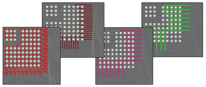
Altium Designer includes excellent surface mount component fanout tools, which also support BGA escape routing. The escape routing engine will attempt to route each pad out to just beyond the edge of the device - making routing connections to them much easier.
Fanout and escape routing is launched from the Route » Fanout sub-menu of the main menus or using the Component Actions » Fanout Component command from the component's right-click menu.
-
The Route » Fanout » All command is used to fanout the pads of all surface mount components in the current design that connect to both signal and power plane nets. This procedure can be particularly useful in determining whether a design - especially a complex, high-density design - is likely to be successfully routed when passed to the Autorouter.
Running this command is equivalent to running both the Fan out Signal and Fan out to Plane passes in a strategy defined for the Autorouter.
-
The Route » Fanout » Power Plane Nets command is used to fanout the pads of all surface mount components in the current design that connect to power plane nets.
Running this command is equivalent to running the Fan out to Plane pass in a strategy defined for the Autorouter.
-
The Route » Fanout » Signal Nets command is used to fanout the pads of all surface mount components in the current design that connect to signal plane nets.
Running this command is equivalent to running the Fan out Signal pass in a strategy defined for the Autorouter.
-
The Route » Fanout » Net command is used to fanout all SMT component pads connected to a chosen net.
Running this command is equivalent to running either the Fan out Signal or Fan out to Plane pass in a strategy defined for the Autorouter depending on whether you have chosen a signal or power plane net.
If you do not know the location of a pad on the net, or one of its connection lines, click in free space and the Net Name dialog will pop up, prompting for the net name. If you are unsure of the net name, type ? then click OK to launch the Nets Loaded dialog, which lists all loaded nets for the design. The SMT component pads for the net you choose in the dialog will be fanned out (where possible) when you click OK.
-
The Route » Fanout » Connection command is used to fanout all SMT component pads in a chosen connection.
Running this command is equivalent to running either the Fan out Signal or Fan out to Plane pass in a strategy defined for the Autorouter depending on whether the connection you have chosen is associated with a signal or power plane net.
-
The Route » Fanout » Component command is used to fanout the pads of the chosen surface mount component that connect to both signal and power plane nets.
Running this command is equivalent to running both the Fan out Signal and Fan out to Plane passes in a strategy defined for the Autorouter.
If you do not know the location of a component, click in free space and the Component Designator dialog will pop up, prompting for the component name. If you are unsure of the component name, type ? then click OK to launch the Components Placed dialog, which lists all components for the design. The pads for the SMT component you choose in the dialog will be fanned out (where possible) when you click OK.
If a component contains pads that are not connected to any nets, a dialog will appear asking if you wish to fanout these pads as well.
-
The Route » Fanout » Selected Components command is used to fanout the pads of the selected surface mount components that connect to both signal and power plane nets.
Running this command is equivalent to running both the Fan out Signal and Fan out to Plane passes in a strategy defined for the Autorouter.
If a component contains pads that are not connected to any nets, a dialog will appear asking if you wish to fanout these pads as well.
-
The Route » Fanout » Pad command is used to fanout the chosen SMT component pad that connects to either a signal or power plane net.
Running this command is equivalent to running either the Fan out Signal or Fan out to Plane pass in a strategy defined for the Autorouter, depending on whether the pad is connected to a signal or power plane net.
-
The Route » Fanout » Room command is used to fanout the pads of all surface mount components in the chosen room that connect to both signal and power plane nets.
Running this command is equivalent to running both the Fan out Signal and Fan out to Plane passes in a strategy defined for the Autorouter.
-
The Component Actions » Fanout Component command from the right-click menu of the required component (selected or not) in the design space is used to fanout the pads of the surface mount component currently under the cursor, that connect to both signal and power plane nets.
Running this command is equivalent to running both the Fan out Signal and Fan out to Plane passes in a strategy defined for the Autorouter.
If a component contains pads that are not connected to any nets, a dialog will appear asking if you wish to fanout these pads as well.
Fanout Behavior
Used inner pads are first fanned out using the traditional dog-bone (a short route with a via on the end) to access another layer, and then from the via they are escape routed out just beyond the edge of the device, working through the available routing layers until all pads have been escape routed.
Fanout and escape routing is done in accordance with the applicable design rules, including the Fanout Control rule, Width rule (for additional track laid down), Routing Via Style rule (for dropped fanout vias), Routing Layers rule, and the Clearance rule. A report of all pads that could not be escape routed will be generated and opened, click on an entry in the report to cross probe to the PCB and examine that object.
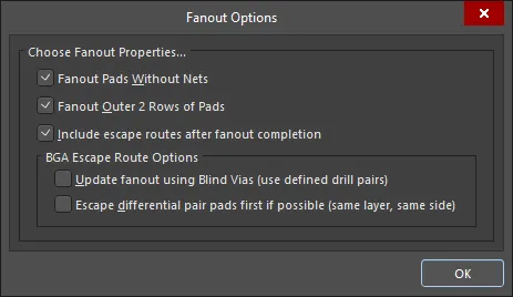
After selecting a fanout command, the Fanout Options dialog will open. The dialog includes controls that let you specify fanout and escape routing options, as well as options for using blind vias (configured in the Via Types tab of the Layer Stack Manager). Other options include fanning out the outer two rows of pads in addition to the inner (and harder to get to) rows, and only pads that have nets assigned to them.

Use the Fanout Options dialog to control fanout and escape routing options.
Options and Controls of the Fanout Options Dialog
Choose Fanout Properties
- Fanout Pads Without Nets - enable this option to fanout pads from the component even if they have no nets assigned to them. When this option is disabled, only pads with nets assigned will be fanned out.
- Fanout Outer 2 Rows of Pads - enable this option to fanout pads from the component including the outer two rows (which are usually easily routed).
Fanning out a component will drop vias as required to enable connection. If drill-pairs have been configured for layers and the Update fanout using Blind Vias option is enabled, blind vias will be dropped, otherwise, through-hole vias will be used.
- Include escape routes after fanout completion - enable this option to add escape routing to each fanout. Escape routing places tracks onto the fanout vias and component pads, bringing them out to the edges of the component, to make routing connections to them easier.
BGA Escape Route Options
The options in this region of the dialog only become available when the Include escape routes after fanout completion option is enabled.
- Update fanout using Blind Vias (BGA escape routing only) - enable this option to drop blind vias between configured drill-pair layers in the layer stack. When this option is disabled, only through-hole vias will be dropped regardless of drill-pair layer settings.
If there are no drill layer pairs defined to be able to use blind vias, this option will appear as Cannot Fanout using Blind Vias (no layer pairs defined).
- Escape differential pair pads first if possible (same layer, same side) - enable this option to fanout and escape route any assigned differential pair nets together, and before performing other fan out operations, effectively keeping their routes together. The fanout will place escape routing tracks on to the same layer and as adjacent as possible.

Example of fanout and escape routes for a 1mm pitch BGA.
- If you use any of the fanout commands before autorouting the board, there is no need to lock the preroutes unless you have additional manual routing or have modified the fanout routing in some way.
- To fanout the pads of a component, make sure that there is no polygon pours under this component on any layer. Polygons can be shelved before creating fanouts and restored afterward.