Printed Electronic Design
An exciting evolution in the design and development of electronic products is the ability to print the electronic circuit directly onto a substrate, such as a plastic molding that becomes a part of the product.
|
|
These slides show the 2D and 3D views of an example printed electronics layout. (Image courtesy of "csi entwicklungstechnik" from their design utilizing TactoTek® In-Mold Structural Electronics).
|
This surface-oriented implementation technique is referred to as Printed Electronics. While the term Printed Electronics is not a precise description of the technology, as printing is not the only technique used to create it, the term has broad industry acceptance and will be used on this page.
There are a number of approaches being developed to create printed electronics, including: 3D printing with conductive inks; stamping techniques that can create conductors as well as simple circuit elements, such as transistors; and laser deposition techniques that can build up conduction paths at very small scales, with ultra-high precision.
Printed electronics will become a pivotal technology, allowing the integration of electronics into new markets. Printed electronics allow an intimate connection between the circuit and the product. From a flexible sensor that attaches directly to the body, through to a multi-sensor, finger tip-shaped molding that allows a robotic hand to hold a soft plastic cup as liquid is poured into it, printed electronics will allow innovative new solutions to be developed across many market segments.
The Technology
In terms of what the technology delivers, the game remains the same - electronic components are connected together via conductive pathways, forming an electronic circuit that performs a useful function. What differs is the approach used to build up the circuit.
The layer-oriented fabrication technology used to make a traditional PCB is a reductive process. Each conductive layer starts as a continuous sheet of conductive material, such as copper, which is then etched away, leaving only the copper that forms the required conductive pathways. It is also a multi-staged process, as the individual conductive layers are sandwiched together with alternating layers of insulation, and various drilling and post-plating processes applied.
Printed electronics is an additive process, the signal pathways are printed directly onto a substrate. If a subsequent signal pathway needs to cross an existing pathway, a small patch of insulation is printed directly in the required location. Acting as a tiny bridge, it allows the new signal pathway to be printed across the existing pathway, without connecting to it. As an example, if the design is using the DuPont InMold technology, the circuit is first printed onto a flat plastic substrate, which is then thermoformed and injection molded into the final product shape.
Using printed electronics, the humble rigid fiberglass printed circuit board substrate is no longer required. Instead, the circuit is formed directly as a part of the product, the conductors ultimately following the shape and contours of the product's surface. As there is less material used and less waste, printed electronics will ultimately become a more cost-effective approach than a traditional PCB, in many situations.
NOTE - at this stage, only flat substrate surfaces are supported by the printed electronics design functionality in Altium Designer. For fully 3D circuit design, Altium Designer's dedicated 3D-MID design tool is available now.
Refer to the True 3D-MID Design feature page for an overview of the functionality.
Refer to the 3D-MID Design documentation page to learn more.
Designing Printed Electronics in Altium Designer
Apart from the substrate that the design is printed on, there are no physical layers in a printed electronics product - conductive pathways are printed directly onto the substrate. Where the design requires pathways to cross over each other a small patch of dielectric material is printed in that location, sufficiently expanded beyond the crossover to achieve the required level of isolation between the different signals.
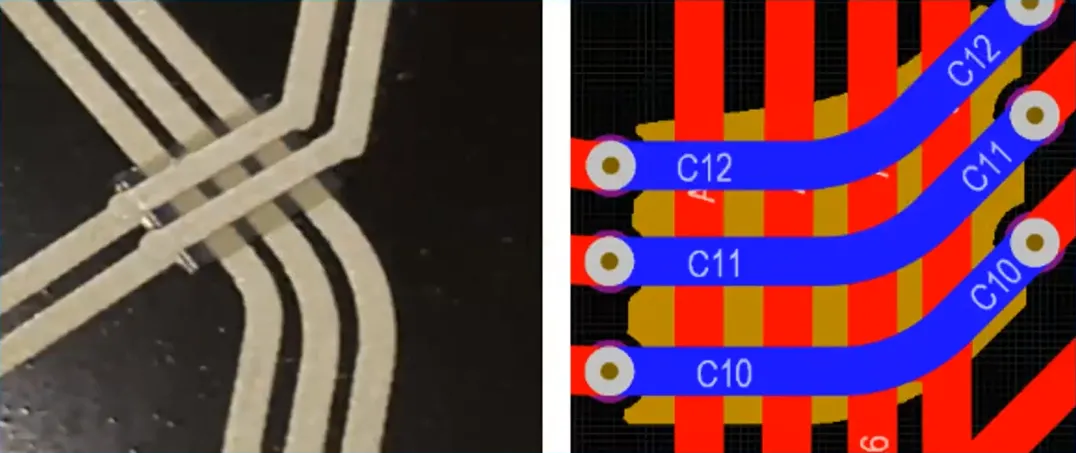
The outputs required to drive the printing process are generated using a standard output format, such as Gerber.
The outputs will include a file for:
-
Each conductive printing pass - essentially the same as a copper routing layer in a traditional PCB
-
Each dielectric printing pass - since dielectric patches are printed, their shapes are also specified in an output file, such as a Gerber file.
Defining the Layer Stack
So how are these multiple printing passes defined in the PCB editor? In printed electronics, each printing pass requires an output file, so rather than thinking of it as a series of copper layers separated by dielectric layers, think of it as a set of printing passes, with each pass either being a conductive layer of ink, or a non-conductive layer of ink.
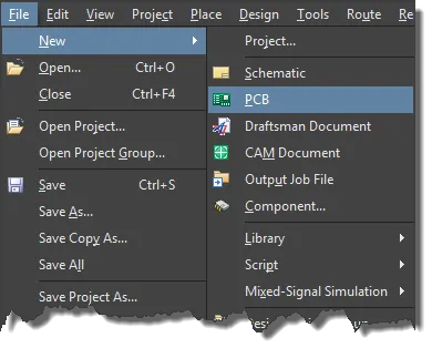
To create a printed electronics design, first create a new PCB using File » New » PCB from the main menus.
Configuring a new board as a printed electronics design is done in the Layer Stack Manager. Choose Design » Layer Stack Manager from the main menus to access the Layer Stack Manager. Use the  drop-down then select Printed Electronics or select Tools » Features » Printed Electronics from the main menus.
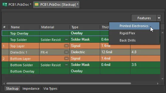 A new PCB defaults to two copper layers, separated by a dielectric layer.
When the Printed Electronics feature is enabled, the dielectric layer between the two copper layers disappears. Why? Because printed electronics require an output file for every layer, so dielectric layers are not used as they are not used to generate output files.
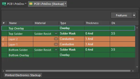 When the Printed Electronics feature is enabled, the dielectric layer is removed.
Instead, non-conductive layers are added. Dielectric shapes, referred to as patches, can be manually or automatically defined on these layers where ever signal paths need to cross each other on the conductive layers.
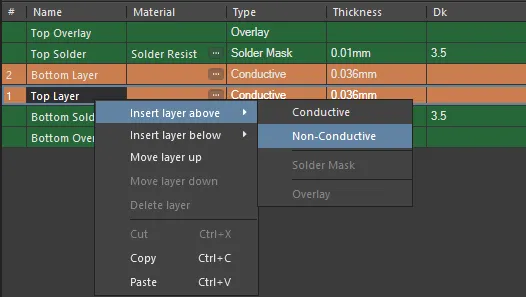
Non-Conductive layers can be inserted between the Conductive layers, and dielectric patches defined on them.
Right-click on a layer to insert a layer above or below, move a layer up or down, or delete a layer. Printed electronics do not use the Bottom Solder or Bottom Overlay; these have been removed.
Once the layers have been added, set the properties of the material for each layer.
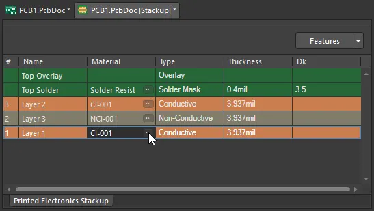 Use the ellipsis button to select the material to use for each printed layer.
Material Selection
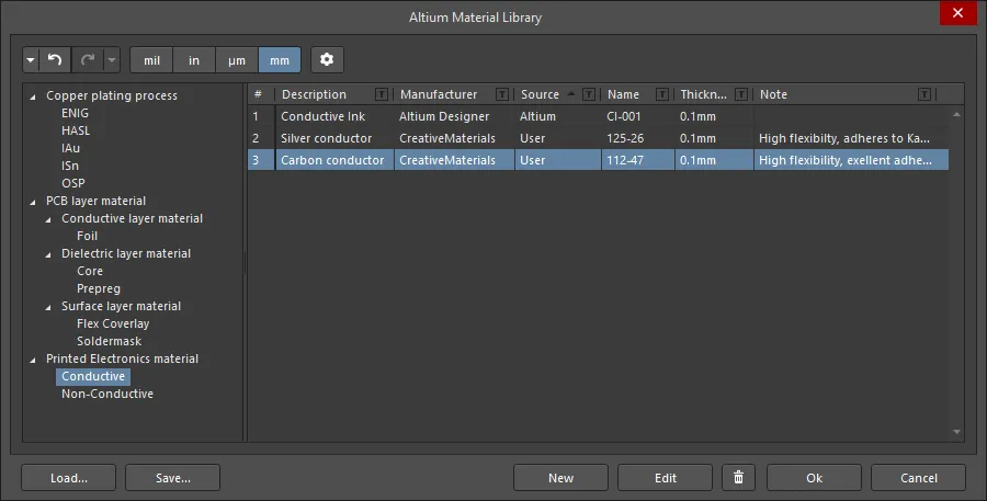
The material used in both traditional PCB design and printed electronic design are selected in the Layer Stack Manager's Material Library.
When the Layer Stack Manager is open, use the Tools » Material Library command to open the Altium Material Library dialog.
-
The Altium Material Library dialog includes materials for both conductive and non-conductive layers.
-
New materials can be defined in the library, click the New button at the bottom of the dialog. If user-defined materials are created, they can be saved to and loaded from a user-defined materials library.
-
To select a material for a specific layer, click the ellipsis control (
 ) in the Material cell for that layer in the Layer Stack Manager. The Select Material dialog will open, displaying only the materials that are suitable for that layer Type. Select the required material and click OK.
Properties Panel
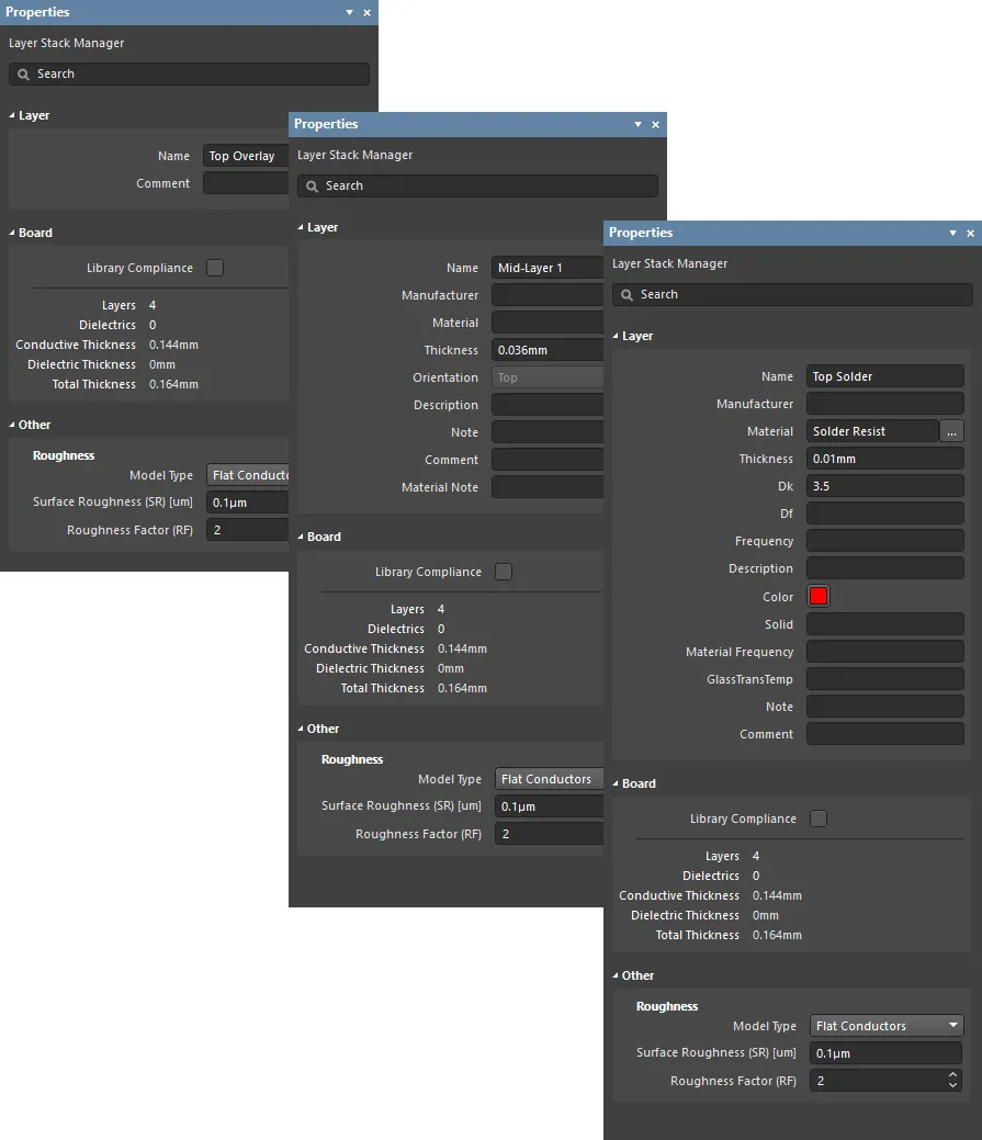
When the Printed Electronics Stackup tab of the Layer Stack document is active, the Properties panel allows you to edit and configure the layer properties of the Layer Stack for a printed design.
-
Layer
-
Name – the name of the layer.
-
Manufacturer – the layer manufacturer.
-
Material – the layer material. This can be pre-defined in the Altium Material Library dialog (Tools » Material Library) in the Constructions field, or user-defined in the Layer Stack. Click
 to open the Select Material dialog to choose the desired material for the currently selected layer in the layer stack.
-
Thickness – the thickness of the signal layer.
-
Dk – this is the Dielectric Constant (also referred to as εr in electromagnetics). This indicates the relative permittivity of an insulator material, which refers to its ability to store electrical energy in an electric field. For insulating purposes, a material with lower dielectric constant is better and in RF applications, a higher dielectric constant may be desirable. In addition, the lower the relative dielectric constant, the closer the performance of the material to that of air. This property is critical to matching the impedance requirements of certain transmission lines.
-
Df – this is the Dissipation Factor. This indicates the efficiency of insulating material by showing the rate of energy loss for a certain mode of oscillation, such as mechanical, electrical, or electromechanical oscillation. In other words, this is the property of a material that describes how much of the energy transmitted is absorbed by the material. The greater the loss tangent, the larger the energy absorption into the material. This property directly impacts the signal attenuation at high speeds.
-
Frequency – this is the frequency at which the material is tested and the value that Dk / Df correspond to a certain frequency. Frequency is also taken from material references.
-
Description – enter a meaningful description.
-
Color – this is the required color of the solder mask. Click to open a drop-down to set/change the color.
-
Solid – N/A
-
Material Frequency – N/A
-
GlassTransTemp – this is the Glass Transition Temperature (also known as TG) and is the temperature at which the resin changes from a glass-like state to an amorphous state changing its mechanical behavior, i.e. expansion rate.
-
Note – enter any pertinent notes for the layer.
-
Comment – enter any necessary comments for the layer.
-
Board
-
Library Compliance – when enabled, for each layer that has been selected from the Material Library, the current layer properties are checked against the values of that material definition in the library.
-
Layers – the number of conductive layers.
-
Dielectrics – the number of dielectrics.
-
Conductive Thickness – this is the sum of the thicknesses of all signal and plane layers (all copper or conductive layers).
-
Dielectric Thickness – the thickness of dielectric layer(s).
-
Total Thickness – the total thickness of the finished board.
-
Other
Roughness – shows roughness of conductive layers.
-
Model Type – preferred model for calculating the impact of surface roughness (refer to the articles below for more information on the various models). Applies to all copper layers in the stack.
-
Surface Roughness – value of the surface roughness (available from your fabricator). Enter a value between 0 to 10µm, default is 0.1µm
-
Roughness Factor – characterizes the expected maximal increase in conductor losses due to the roughness effect. Enter a value between 1 to 100, default is 2.
Routing the Nets
-
The nets in a printed electronics design are routed in the same way as a traditional PCB, using the Interactive Routing command.
-
Conductive layer transitions are performed using the + and - keys on the numeric keypad, or the Ctrl+Shift+Wheelroll shortcut.
-
When you change layers during routing a via is added, the via properties are determined by the applicable Routing Via Style design rule.
Are Vias Needed?
The software needs to place a via to maintain the connectivity of the net during routing, and also to manage the connectivity when the routing is modified by pushing or dragging. Vias are not needed for layer-to-layer connectivity, the software assumes that overlapping tracks on different layers are connected.
The vias can have their diameter set to the same size as the routing width.
Increasing the Route Thickness
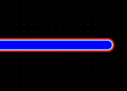
The route thickness can be built up if required, for example, to implement a structure such as a printed antenna. This is achieved by placing multiple routes on top of one another, on different conductive layers.
Adding Dielectric Shapes
Once the nets have been routed, the next step is to create the dielectric patches needed to separate any different-net crossovers. Dielectric shapes are defined on non-conductive layers. They can be defined manually, or automatically created using the Dielectric Shapes Generator.
Manual shapes can be created from Arcs, Lines, Fills, or Solid Regions. Solid Region objects offer the greatest flexibility, as their edges can be adjusted to create virtually any shape.
Dielectric Shapes Generator
The software also includes an automatic Dielectric Shapes Generator. The concept here is to first complete the routing as required on conductive layers, placing vias to switch between layers.
To access the Dielectric Shapes Generator in Altium Designer, the Printed Electronics Crossover Generator software extension must be installed. This extension can be installed or removed manually.
For more information about managing extensions, refer to the Extending Your Installation page (Altium Designer Develop, Altium Designer Agile, Altium Designer).
When the routing is complete, run the Tools » Printed Electronics » Generate Dielectric Patterns command to open the Dielectric Shapes Generator dialog. When the Dielectric Shapes Generator is run, it will remove all shapes on the target layer(s), then recreate them. If shapes have been defined manually, lock them before running the Dielectric Shapes Generator.
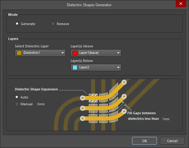
Options and Controls of the Dielectric Shapes Generator Dialog
-
Mode - select the desired mode:
-
Generate - select to generate new dielectric patches for all enabled layers specified in the Layers region.
-
Remove - select to remove any existing shapes the generator detects on the layers specified in the Layers region before it adds its own.
-
Layers - the generator will identify all crossovers and add dielectric patches in accordance with the settings in this region of the dialog.
-
Select Dielectric Layer - use the drop-down to select the dielectric layer. If All is selected, the generator looks for cross-overs on any pair of conductive layers and puts a patch on a dielectric layer that is between those two conductive layers. If no dielectric layer is selected, dielectric shapes will be created for all crossovers between all layers on appropriate dielectric layers. Use the Layer(s) Above and Layer(s) Below to choose which two conductive layers you want the generator to look between when it is searching for cross-overs. If it finds an object on Layer(s) Above that crosses over an object on Layer(s) Below, it generates a patch to place between them and places it on the layer that is specified in the Select Dielectric Layer region. The Layer(s) Above and Layer(s) Below options are not available if Remove is selected in the Mode region.
-
Dielectric Shape Expansion
-
Auto - in this mode, the dielectric shape is automatically expanded to satisfy the requirement of the applicable Clearance Constraint design rule.
-
Manual - in this mode, the generator builds a shape to match the shape formed by the crossed-over objects, then expands that shape out by the distance entered. For example, using this mode, if there are two tracks on different layers that are too close for the clearance violation, a patch will not be placed.
-
Fill Gaps between dielectrics less than <xx> - specify a measurement if you want gaps filled between dielectrics that are less than a number you specify. This can be used to merge adjacent dielectric patches into larger patches.
Net Connectivity and Design Rule Checks
Online DRC is not supported when the layer stack is configured as Printed Electronics because of the different logic used to define violation conditions; such as nets crossing on different layers being flagged as a short circuit. Once the routing is complete and the isolation patches have been defined, click the Run Design Rule Check button in the Design Rule Checker dialog (Tools » Design Rule Check) to perform a batch DRC.
Notes about net connectivity and Design Rule Checks:
-
When a net needs to switch to another conductive layer, insert a via. This ensures that the track segments are correctly handled if the routing is dragged or pushed.
-
Touching/crossing tracks that are on different layers are considered connected. If they are in the same net this is not flagged as a broken net, if they are in different nets this is flagged as a short circuit.
-
A dielectric shape is required to isolate touching/crossing tracks, this shape is placed on a non-conductive layer. The dielectric shape can be placed manually, or by the Dielectric Shape Generator. The dielectric shape must extend beyond the edges of the crossing tracks sufficiently to satisfy the applicable clearance constraint design rule.
-
For a printed electronic design, design rule checks for short-circuits, clearance violations, and unrouted nets behave as described below.
Short Circuit Design Rule
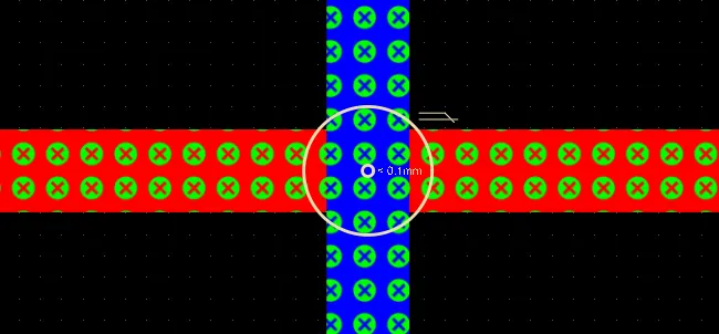
In a Printed Electronics design, when different nets cross over on different layers, they are flagged as a short circuit. These cross-overs are isolated by placing a dielectric patch on a non-conductive layer.
Clearance Design Rule
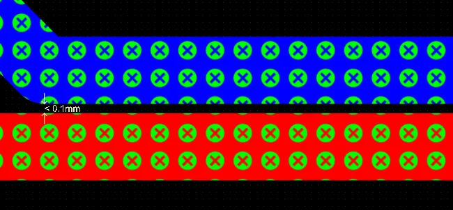
Net to net clearances are tested on all layers, not just the same layer.
Unrouted Net
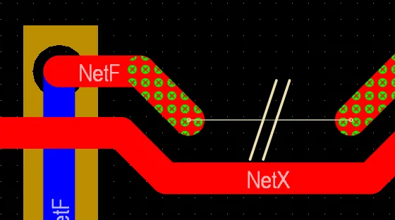
Layer transitions do not require a via, the net analyzer will recognize that the net is not broken.